

Light-Emitting Diodes for Energy Harvesting


1
SDLab—Semiconductor Device Lab, Department of Industrial, Electronic and Mechanical Engineering, Roma Tre University, Via Vito Volterra 62, 00146 Rome, Italy
2
NooEL—Nonlinear Optics and OptoElectronics Lab, Department of Industrial, Electronic and Mechanical Engineering, University Roma Tre, Via della Vasca Navale 84, 00146 Rome, Italy
*
Author to whom correspondence should be addressed.
Electronics 2024, 13(8), 1587; https://doi.org/10.3390/electronics13081587
Submission received: 26 March 2024
/
Revised: 17 April 2024
/
Accepted: 18 April 2024
/
Published: 22 April 2024
(This article belongs to the Special Issue Energy Harvesting and Energy Storage Systems, 3rd Edition)
Abstract
:Energy harvesting is gaining substantial relevance in the realm of ultra-low-power electronics and Internet-of-Things devices with limited access to classic power sources. Several harvesting approaches are available, depending on the energy source; among them, photovoltaic devices benefit from the highest energy density. However, the inclusion of a dedicated photovoltaic cell in a low-power system may result in increased costs and complexity, thus hampering economic sustainability. Conversely, electronic apparatuses often make use of light-emitting-diodes (LEDs), which could be effectively employed as photovoltaic energy harvesters whenever not actively generating photons. Here, we explore the potentials of commercially available LEDs for energy harvesting and determine their quantum efficiency. We examine the correlation of the latter with the spectral response and the available light, demonstrating that visible-wavelength diode emitters can yield very high conversions in the photovoltaic mode. We report measured quantum efficiencies as high as 39% under low-intensity (100 µW/cm2) fluorescent illumination.
1. Introduction
The ever-increasing energy quest and attention to environmental issues have long promoted the development of large-scale green and renewable energy generators, including photovoltaic, wind, hydroelectric, and geothermal systems.
In the last couple of decades, devices and technologies for small-scale energy harvesting have also gained considerable relevance [1]. Such interest has been stimulated by the surge in the usage of ultra-low-power electronics and the advent of the IoT paradigm, where several electronic devices are distributed and wirelessly connected, often without access to physical power lines. In this context, small-scale energy harvesters can reliably supply the limited amount of required power (<1 mW).
Energy harvesting aims at converting into electrical the energy available in the environment from sources otherwise wasted, including optical [2], mechanical [3], thermal [4], and electromagnetic [5] sources. Its potentials clearly depend on the source intensity and the achievable conversion efficiency (i.e., the ratio between the electric power output and the total power input from the relevant energy source). Typical values are reported in Figure 1 for the most relevant cases [1,6,7,8]. Mechanical power densities are available between 20 µW/cm2 and 1 mW/cm2, with corresponding conversion efficiencies from 1 to 10%. Thermal sources can provide intensities of up to 1 mW/cm2, but only less than 3% can be converted into electric power. Electromagnetic power densities are even lower (1 to 50 µW/cm2), but the obtainable conversion efficiency can reach 50%. Optical sources provide much larger densities from 0.1 to 100 mW/cm2, resulting in harvested energy with conversion efficiencies from 5 to 30%.
Despite the usually low energies, these values are often sufficient for applications including remote sensing, sensor networks, tracking and identification systems, safety and security equipment, wearable and implanted electronics, and smart cards [9,10]. As otherwise stated, micro-energy harvesting is very effective whenever it can cancel/bypass the need for running power cables to remote or hardly reachable locations or else can avoid replacing expensive primary batteries.
It is apparent from Figure 1 that the most promising approaches are based on using optical radiation. Nowadays, several products are powered in this fashion and exploit small solar cells as harvesting devices, from smart watches to wearable sensors, from pocket calculators to shelf labels, and so on.
Solar cells are generally designed and optimized for outdoor applications and perform rather poorly when used indoors owing to the significantly different spectrum in the latter case as compared to the solar one. This has triggered the realization of devices for indoor energy harvesting, resorting to semiconductor materials that benefit from band-gap engineering in order to match their spectral response to the light source [11,12]. Moreover, given the small power budget available and market/economy considerations, low-cost solutions have to be developed that involve materials well known and tested in the microelectronics industry. Some approaches for the development of low-cost photodetectors and based on non-silicon materials have been proposed in the past, but the overall economic budget of such systems is still not suitable for the mass production of energy harvesters [13]. In this context, several researchers have recently explored the possibility of using light-emitting-diodes (LEDs) to harvest energy from both indoor and outdoor illumination, counting on the fact that such semiconductor elements are widespread and inexpensive. LEDs, while designed to convert electric currents into photons, can operate in reverse, i.e., converting a photon flux into electric power, just like photovoltaic solar cells. In addition, due to the large variety of employed semiconductors and emitted wavelengths, LEDs can respond in different spectral ranges.
Horvat and coworkers developed an LED-powered identification tag consisting of an energy-harvesting LED array, a power management circuit with a storage capacitor, and a microcontroller, demonstrating the possibility of feeding the latter and an output LED [14]. The energy-harvesting capability of several LEDs exposed to sun light has been evaluated and reported, demonstrating powers of up to 2.7 W harvested from a 96 × 216 LED display employing a DC–DC converter [15]. Other notable examples are the demonstrations of very low-cost battery-less sensor nodes [16] and mobile terminals [17] powered by LEDs, an LED image sensor with both energy-harvesting and imaging capabilities [18], a harvesting system that generated more than 400 µW under tube and bulb light illumination and included arrays of infrared LEDs, a power management unit, and a supercapacitor [19].
Even though plenty of demonstrations are available in the literature and illustrate the effectiveness of LEDs as light energy harvesters, no systematic studies are available that describe the dependence of the energy conversion efficiency both on the LED characteristics (e.g., the peak emission wavelength) as well as on the illumination (e.g., sun, LED, halogen lamps, etc.). Such knowledge is deemed paramount for optimizing the efficiency of LED-based energy harvesters and, indeed, the main motivation of the work reported in the following sections. In this paper, we report on the systematic investigation of the characteristics and energy harvesting potentials of several (visible and near-infrared) LEDs when illuminated by various sources such as solar radiation, fluorescent tubes, LEDs, and halogen lamps.
2. Materials and Methods
The schematic cross-sections of a silicon solar cell and of an AlInGaP LED are shown in Figure 2. The photovoltaic device and the LED architectures are significantly different in term of size and doping profiles.
Typical Si solar cells are n+p junctions with a highly doped and thin (a few hundred nanometers) n+ emitter and a thick (a few hundred micrometers) p-type base that serves as the active layer. The power conversion efficiency mainly depends on the large thickness of the base and its low recombination rate, the latter being achieved with an optimal doping density (typically in the 1017/cm3 range) resulting from a tradeoff between the carrier diffusion length and the inverse saturation current. In addition, the top of the solar cell is provided with a wideband antireflection coating (ARC) and/or a texturized surface [20]. Solar cells built from other semiconductor materials (e.g., III–V, thin-film chalcogenide, perovskites, etc.) share a similar structure but can typically ensure satisfactory efficiencies with thinner layers thanks to having much higher optical absorption as compared to Si. Commercially available monocrystalline Si solar cells exhibit (power) conversion efficiencies of between 20 and 25%; thin-film solar cells such as CIGS and CdTe achieve maximum values between 16 and 20% [21]. These efficiencies are typically evaluated with reference to AM1.5G solar illumination and do not apply to other kinds of light sources. Moreover, a solar cell operated with diffused radiation only (as it often happens indoors) is normally less efficient in this situation than under direct illumination due to its poor performance at high incidence angles.
An LED is basically a thin (a few micrometers)-pin double-heterojunction diode wherein the emitting layer is the intrinsic lower-band-gap semiconductor. The doping levels of the pin are usually large to maximize the radiative recombination rate. As visible in Figure 2, the pin diode is deposited on a thick highly doped GaAs substrate and covered with a highly doped current-spreading layer. The LED may have an antireflection coating optimized for its emission wavelength [22]. Such an ARC operates in a bidirectional way, thus allowing for reduced reflectance also when optical radiation impinges onto the LED surface. Consequently, LEDs equipped with antireflection layers may exhibit enhanced energy harvesting close to their nominal emission wavelength.
Standard compounds used in active layers are AlGaAs, AlGaInP, and InGaN for LEDs operating in the visible/near-infrared, red/orange/amber, and green/blue/UV, respectively, with essentially similar device structures. In some cases, an insulating substrate is used (typically sapphire) and both contacts can be located on the top surface. The common approach to produce white light is based on one or more phosphors excited by a blue or a UV LED [22].
Despite the significant differences listed above, it has been demonstrated that LEDs can operate as photovoltaic cells. This ability can be ascribed to the large optical absorption of the employed materials (typically III–V direct semiconductors), allowing for an appreciable collection efficiency of the photogenerated carriers even in relatively thin layers. It should be noted, however, that the high doping of the various layers in the LED and the presence of several heterointerfaces increase the chances of charge recombination, thus permitting a good conversion only in a reduced wavelength range wherein the collection efficiency is sufficiently high (i.e., when electron-hole couples are generated in the intrinsic layer or, at most, at a maximum distance corresponding to the diffusion length of minority carriers).
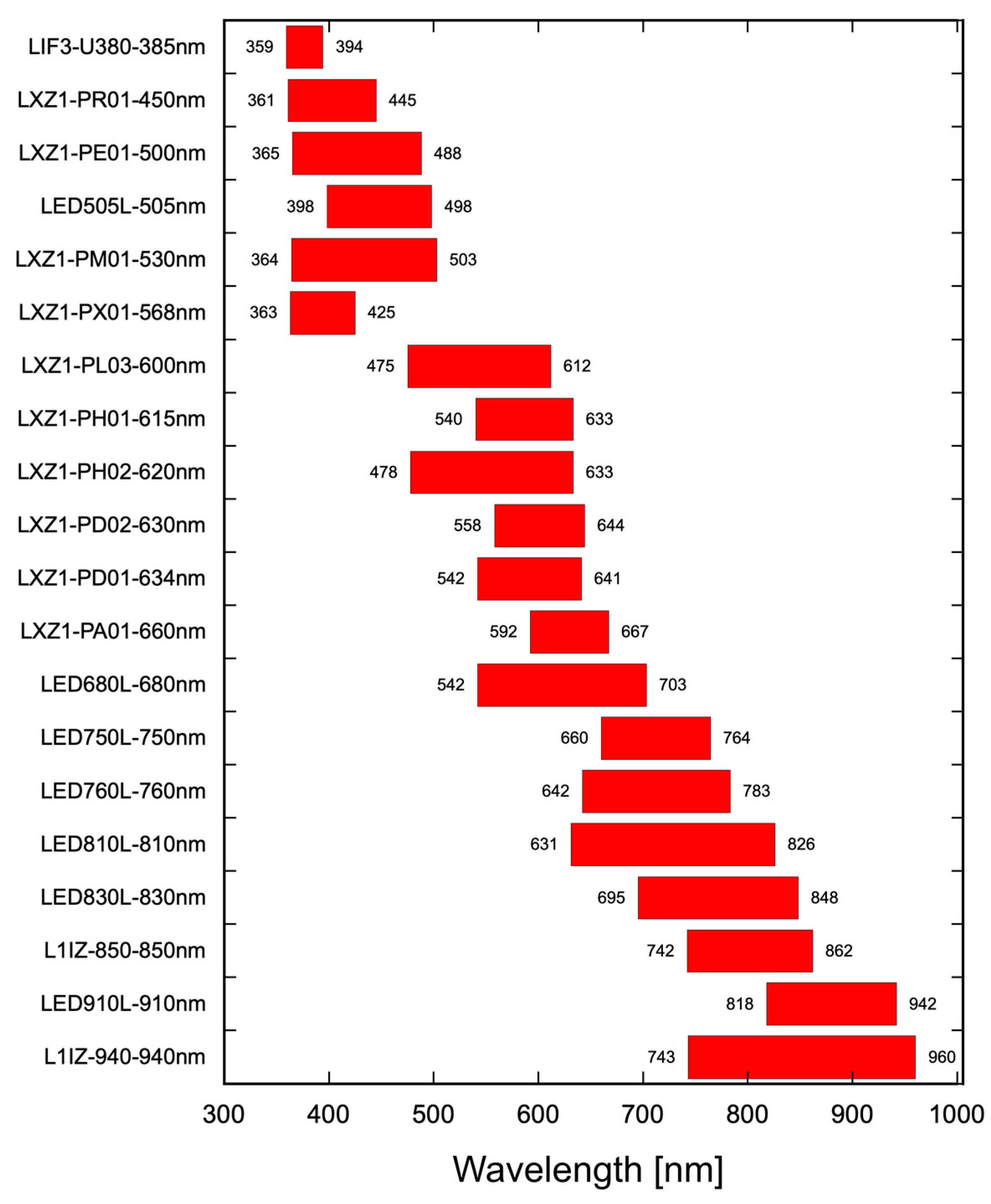
LEDs are available for emission at several wavelengths, resorting to different semiconductors, types of band-gap engineering, and architectures. In our study, we selected 20 LEDs operating in the range from 380 to 940 nm and investigated their performance in terms of spectral quantum efficiency (SQE) and power conversion efficiency (PCE). We also included the white LED K691B, which is a device typically employed for indoor lighting and based on a blue-emitting LED covered with a phosphor. All the selected LEDs are off-the-shelf commercial types with a 1 mm2 junction area, except the white LED, which has a round surface of diameter 3 mm. The complete list of characterized LEDs is presented in Table 1.
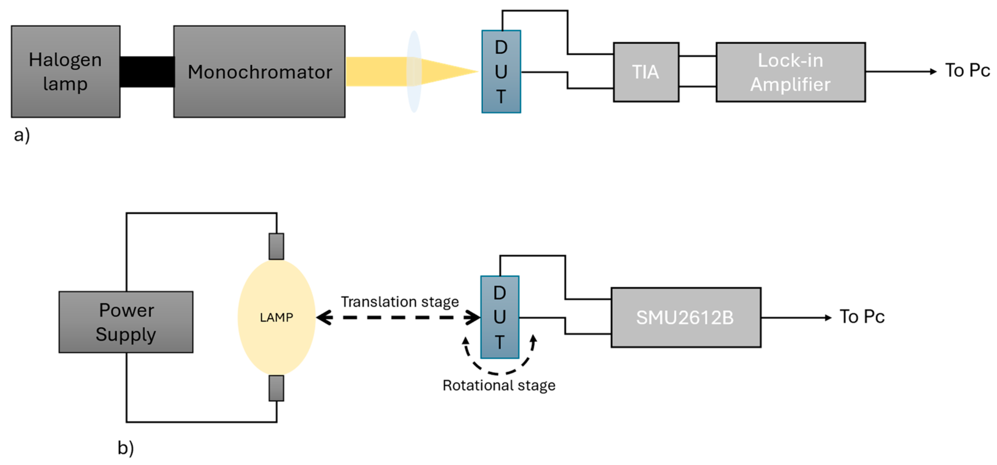
The characterization consisted of evaluating the spectral quantum efficiency and measuring current vs. voltage (I–V) curves and power conversion efficiency under illumination from different light sources. Figure 3b displays the measurement setup for the acquisition of the I–V curves.
The spectral responses were acquired with a calibrated setup based on a Horiba Micro-HR spectrometer and a Stanford SR830 lock-in amplifier. The I–V curves and the PCE were obtained through current–voltage characteristics measured with a KEITHLEY 2612B. The employed light sources were a Lot Oriel class AAB AM1.5G solar simulator; an OSRAM-64628, 3500 K; a 50 W halogen lamp; an OSRAM Lumilux 50 W 4800 lmn fluorescent tube; and a warm Philips (3000 K) 7.3 W LED lamp. The spectral irradiances of the LED and the fluorescent lamps were quantified with the aid of the OCEANINSIGHT Flame-S-VIS-NIR portable spectrometer, the solar spectrum was the ASTM G-173 Air Mass 1.5 G [23], and the halogen lamp spectrum was calculated using the Planck radiation law. The corresponding normalized spectra are displayed in Figure 4.
3. Results and Discussion
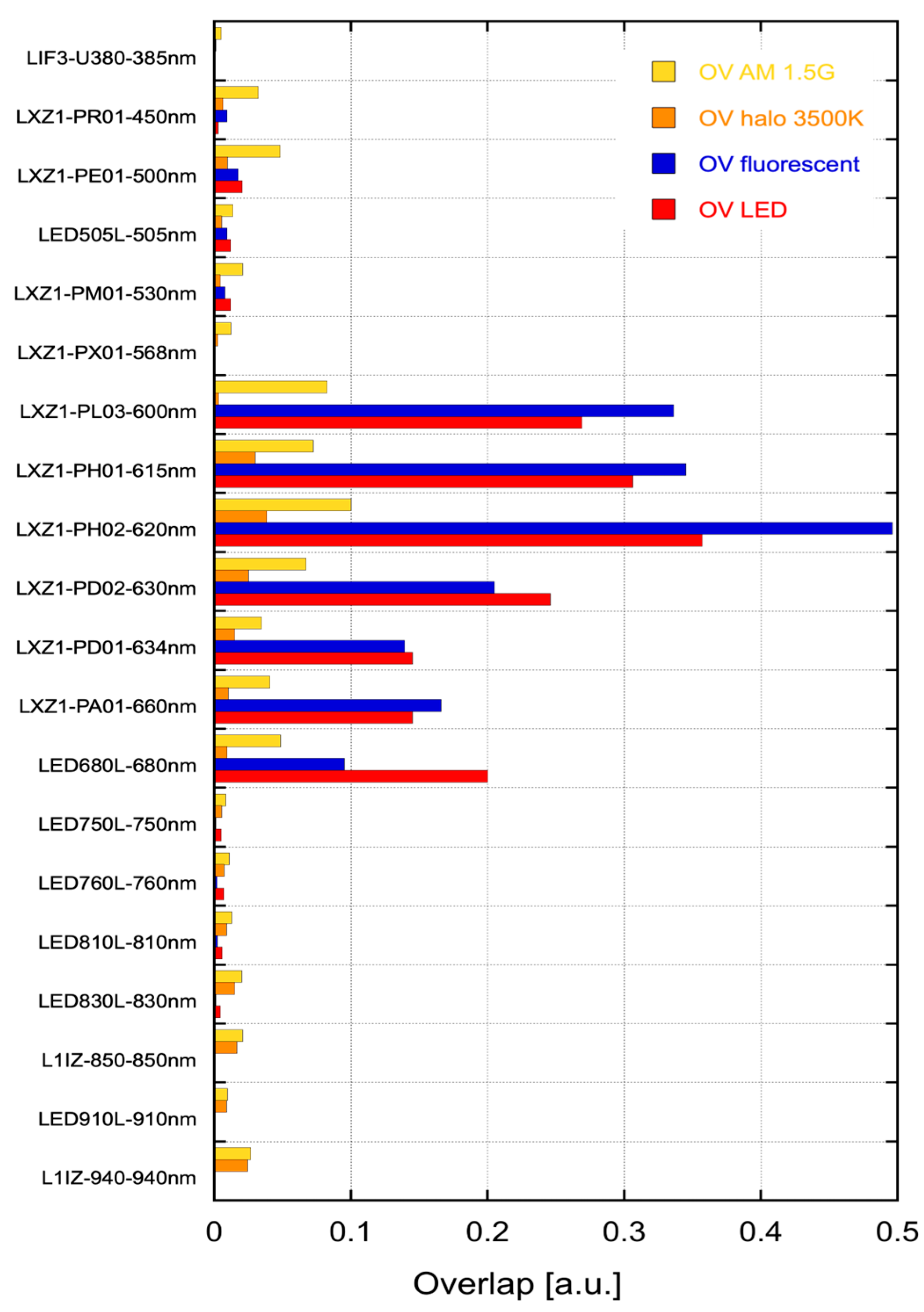
Our investigation started with a preliminary assessment of the LEDs when operated as solar cells. This evaluation was carried out by calculating the overlap integral of the spectral quantum efficiency of each LED with the emission spectrum of the various light sources. The emission spectra of the sources were normalized to yield the same total power in the entire optical band.
The SQE values are graphed in Figure 5a,b. The SQEs were determined as the ratios between the number of electrons extracted from each LED and the number of impinging photons at a specific wavelength. As expected, the SQEs exhibited varying characteristics in terms of highest value, peak wavelength, and bandwidth, with a cutoff close to the LED emission wavelength. The peak SQEs ranged from a minimum of about 20% to a remarkable maximum of above 60%.
The SQE of the white-emitting LED was measured, as well; however, due to its significantly different values, it has been reported in a separate graph in Figure 5b. As expected, the maximum SQE is rather low (about 2.5%) because of the phosphor, which effectively operates as a pumped emitter with high emission efficiency (ηem > 50%) in a standard LED while it behaves as an absorbing filter when the device is used as a solar cell. In addition, the SQE is peaked at 380 nm and its FWHM is relatively small (about 50 nm). Such results are not appealing for photovoltaic applications. For this reason, white LEDs will no longer be discussed in the following sections.
Figure 6 plots the optical bandwidth, calculated using the data from Figure 5a as the wavelength range where the SQE falls below 10% of its maximum. The measured bandwidths range from 35 to 215 nm and, with a few exceptions, longer-emission-wavelength LEDs exhibit broader spectral responses. It is noteworthy that there is a clear correlation between the peak absorption wavelength and the maximum quantum efficiency; the SQE is highest for LEDs operating in the 550–600 nm interval while it decreases towards both shorter and longer wavelengths. This trend can be attributed to either changes in the charge collection efficiency or inefficient absorption due to the wavelength of the impinging radiation. On one hand, at very short wavelengths, the photons are easily absorbed by very thin semiconductor layers, generating photocarriers close to the device surface or to heterointerfaces, where the recombination probability is higher and carrier lifetime is shorter. On the other hand, longer wavelengths require thicker films to be effectively absorbed while the thickness of the absorbing layers in LEDs is typically small, thus not allowing for high quantum efficiency.
The overlap integrals were calculated, integrating the product of the SQEs and the spectra of the light sources over the wavelength range. For the sake of a proper comparison, the lamp spectra were normalized with respect to their integrals in order to make each spectrum represent a light source with the same total output power. The resulting overlap integrals are visible in Figure 7 with reference to four light sources. The figure shows that the most promising devices are LEDs with emission wavelengths between 600 and 660 nm. In addition, most LEDs in this interval exhibit particularly large overlap integrals, with the best performance expected under fluorescent or LED illumination. Finally, some blue-emitting LEDs operate better under sunlight similarly to some infrared LEDs. The higher conversions under LED and fluorescent illumination are quite encouraging as such sources can be easily found indoors. The very high quantum efficiencies expected with the latter confirm that LED-based energy harvesting systems are well suited for the most common indoor applications, a win–win condition.
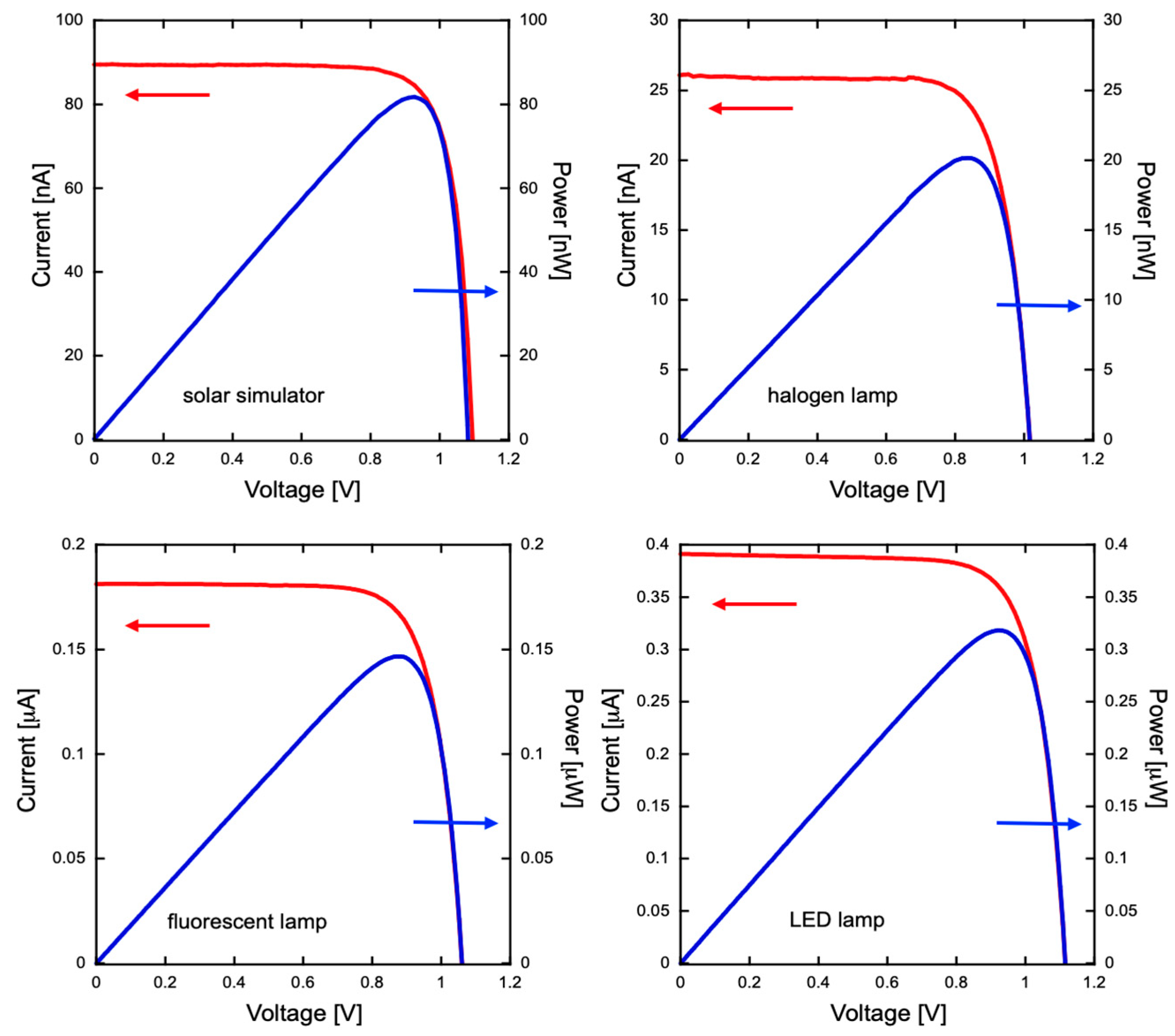
The overlap between LED–SQE and the spectral irradiance of the light sources considers only the device photocurrent whereas it does not account for the voltage contribution to the converted electrical power. Therefore, in order to evaluate the conversion efficiency, the current–voltage (I–V) and the power–voltage (P–V) characteristics were acquired under different illuminations. We tested the most promising devices, as pointed out by the overlap integrals in Figure 7. All I–V curves were measured after setting the sources at the same intensity of 100 µW/cm2, as quantified with a wide-spectral-range thermopile (Thorlabs S302C, Newton, NJ, USA). The I–V and P–V characteristics of LXZ1-PH02 (LED emitting at 620 nm) under various illumination types are presented in Figure 8.
The conversion efficiency η was evaluated at the maximum power point. This device exhibited a remarkably large peak η exceeding 39% under fluorescent light and a more than satisfactory η = 21% under an LED lamp. Another notable example is the LED680L device, which exhibited the highest η = 31% under LED illumination, as apparent in Figure 9.
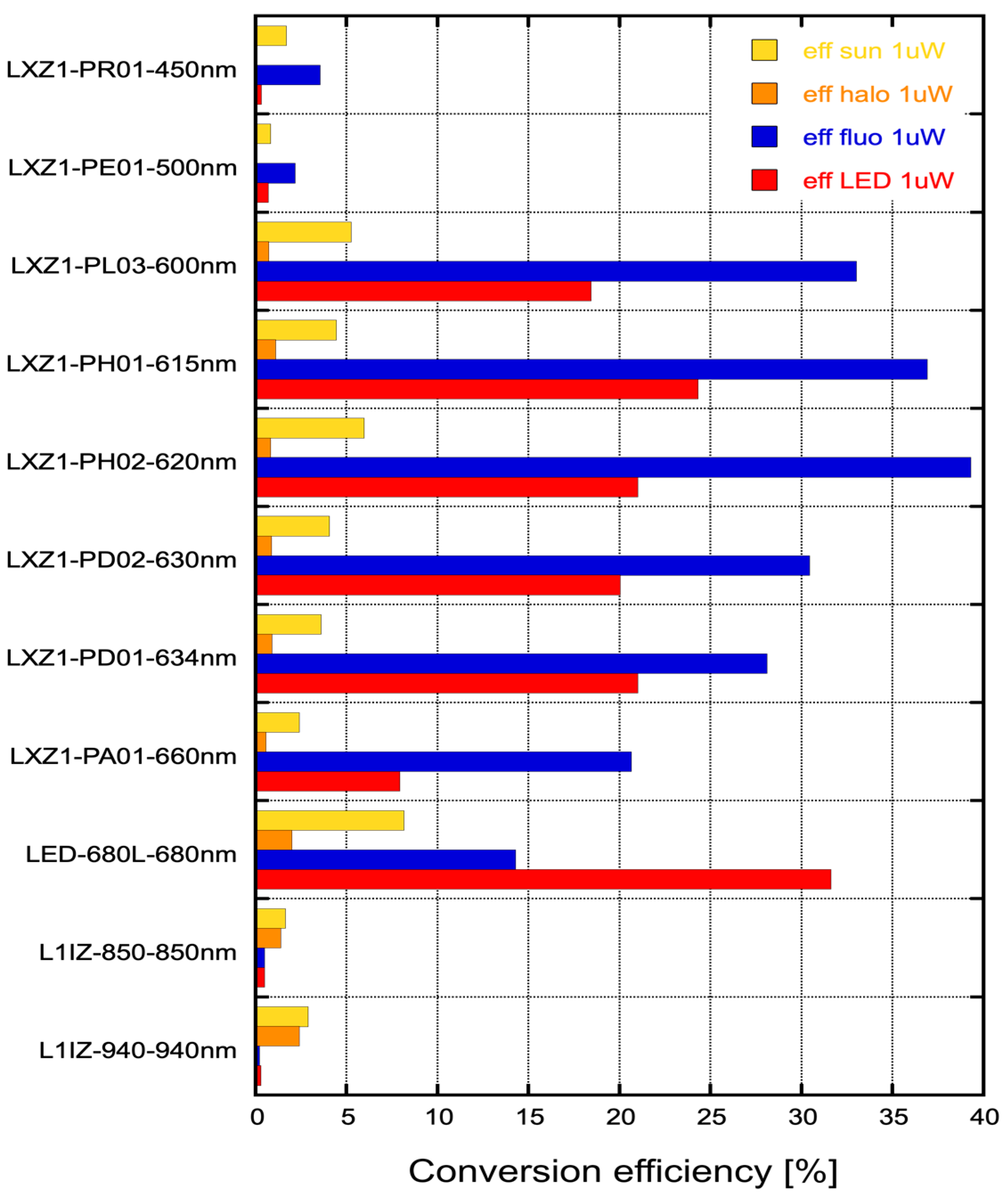
The PCEs of all examined LEDs are summarized in Table 2 in four conditions of illumination, highlighting the highest η for each one. The efficiency data are also graphed in Figure 10. The results are in good agreement with those predicted by the overlap integrals of Figure 7. They confirm that the best performances are associated with LEDs emitting in the 600–680 nm range, with η between 14 and 39% under fluorescent light and η between 8 and 31% under LED light. The largest efficiencies under sunlight and halogen light were 8 and 2.4%, respectively. Such modest values can be ascribed to the poor overlap between the spectral irradiance of the source and the spectral response of the LED, as seen in Figure 4 and Figure 5.
The power conversion efficiencies were measured at a light intensity of 100 µW/cm2, which, in most cases, is rather low even indoors. In fact, 100 µW/cm2 corresponds to 12, 600, 480, and 26 lux for the solar, fluorescent, LED, and halogen sources, respectively. The resulting optical power impinging on the LEDs is 1 µW (device area = 1 mm2).
It is well known that photovoltaic devices exhibit a logarithmic increase in efficiency as the light intensity increases. Therefore, we studied some LEDs under varying light powers. Typical results are shown in Figure 11, graphing efficiency versus power for LXZ1-PH02. The logarithmic trend was confirmed, with efficiency changing at a rate of about 10%/decade, providing information on the actual efficiency to be expected at each illumination level.
Finally, we investigated the role of LED packages on the PCE. LEDs are typically available in two kinds of packages, namely SMD—with a transparent flat surface (intended for wide emission angles)—and TO-18, provided with a plastic or glass lens (intended for small emission angles). When shone on solar cells, the incident light gets concentrated by the lens, but the effect strongly depends on the angle of incidence.
Figure 12 shows the polar pattern of the short-circuit current Isc of two LEDs operating at the same emission wavelength: LED-A is flat while LED-B is in a glass-lensed TO-3 package. Isc was measured using a LED lamp at a distance of 1.5 m from the harvesting LED. As expected, LED-A exhibited a wider pattern and LED-B exhibited a larger photocurrent at normal incidence owing to the lens concentrator. The strong dependence of Isc on the angle suggests that lens-equipped LEDs tend to be less efficient in energy harvesting applications where the light is diffused and accurate LED positioning cannot be ensured.
Therefore, when using LEDs for energy harvesting, the characteristics of the available optical sources (direct or diffused) need be carefully accounted for as well.
4. Conclusions
We have reported the characterization of several LEDs employed as photovoltaic devices for energy harvesting. The availability of optical energy suggests that photovoltaic devices are the best choice for low-power energy harvesting although the implementation of dedicated converters may result in inconvenience from the economic perspective. In this work, we have investigated the use of commercially available LEDs as efficient energy harvesters. While LEDs are widely employed in many applications, from communications to displays, they actively emit light only for brief time intervals with respect to the overall system lifetime. For example, a smartphone display is typically “on” for less than 30% of the total operation of the phone itself, thus suggesting it could be employed as a large area energy harvester in the remaining timespan.
Previous studies on LEDs operated as photovoltaic harvesters did not compare their spectral emission characteristics with the spectra of available light sources, thus neglecting the important role of their overlap. The latter aspect is of the uttermost relevance since low-power energy harvesters would be often employed indoors, where solar radiation is not available and the most common illumination sources are LEDs or fluorescent lamps. We analyzed the harvesting performance of several LEDs under diverse light sources and found that visible-emitting LEDs can reach outstanding conversion efficiencies (i.e., 39%) when operated as photovoltaic devices under fluorescent or LED illumination. We also demonstrated that white LEDs employed for indoor illumination are not well suited for operation as energy harvesters due to both the high energy band-gap of their constitutive materials and the presence of absorbing phosphors that reduce the amount of radiation reaching the junction. We observed that LEDs not equipped with a focusing lens show good performance even when the angle of incidence of the optical radiation is far from the normal, suggesting efficient operation even under indirect, diffused illumination.
At variance with earlier reports on the use of commercial LEDs as energy harvesting devices, we focused on the correlation between the energy conversion efficiency and the type of available illumination. A more detailed analysis of complete energy harvesting systems would have to include the dependance of the overall efficiency on the charge-management circuitry.
As a final note, it should be underlined that the overall power generated by a single LED as a photovoltaic harvester device is normally very low, thus requiring the implementation of efficient charge and battery management systems capable of ultra-low-power operation and low losses.
Author Contributions
The first and third authors, L.C. and A.D.I., equally contributed to the work—from conceptualization to implementation and data acquisition—and to the preparation of the paper. The second author, G.A., contributed by discussing the methods and the results, as well as by editing and reviewing the manuscript. All authors have read and agreed to the published version of the manuscript.
Funding
This research received no external funding.
Data Availability Statement
Data are available upon reasonable request to the corresponding author.
Acknowledgments
E. Diana and G. Macera are kindly acknowledged for their support in some of the reported measurements.
Conflicts of Interest
The authors declare no conflicts of interest.
References
- Bai, Y.; Jantunen, H.; Juuti, J. Energy Harvesting Research: The Road from Single Source to Multisource. Adv. Mat. 2018, 30, 1707271. [Google Scholar] [CrossRef] [PubMed]
- Hao, D.; Qi, L.; Tairab, A.M.; Ahmed, A.; Azam, A.; Luo, D.; Pan, Y.; Zhang, Z.; Yan, J. Solar Energy Harvesting Technologies for PV Self-Powered Applications: A Comprehensive Review. Renew. Energy 2022, 188, 678–697. [Google Scholar] [CrossRef]
- Sezer, N.; Koç, M. A Comprehensive Review on the State-of-the-Art of Piezoelectric Energy Harvesting. Nano Energy 2021, 80, 105567. [Google Scholar] [CrossRef]
- Ando Junior, O.H.; Maran, A.L.O.; Henao, N.C. A Review of the Development and Applications of Thermoelectric Microgenerators for Energy Harvesting. Renew. Sustain. Energy Rev. 2018, 91, 376–393. [Google Scholar] [CrossRef]
- Assogba, O.; Mbodji, A.K.; Karim Diallo, A. Efficiency in RF Energy Harvesting Systems: A Comprehensive Review. In Proceedings of the IEEE International Conference Natural and Engineering Sciences for Sahel’s Sustainable Development–Impact of Big Data Application on Society and Environment (IBASE-BF), Ouagadougou, Burkina Faso, 4–6 February 2020; pp. 1–10. [Google Scholar]
- Vullers, R.J.M.; Van Schaijk, R.; Doms, I.; Van Hoof, C.; Mertens, R. Micropower Energy Harvesting. Solid State Electron. 2009, 53, 684–693. [Google Scholar] [CrossRef]
- Rastegar, J.; Dhadwal, H.S. Energy Harvesting for Low-Power Autonomous Devices and Systems. In Tutorial Texts in Optical Engineering; SPIE: Bellingham, WA, USA, 2017. [Google Scholar]
- Clementi, G.; Cottone, F.; Di Michele, A.; Gammaitoni, L.; Mattarelli, M.; Perna, G.; Lopéz-Suaréz, M.; Baglio, S.; Trigona, C.; Neri, I. Review on Innovative Piezoelectric Materials for Mechanical Energy Harvesting. Energies 2022, 15, 6227. [Google Scholar] [CrossRef]
- Shaikh, F.K.; Zeadally, S. Energy Harvesting in Wireless Sensor Networks: A Comprehensive Review. Renew. Sustain. Energy Rev. 2016, 55, 1041–1054. [Google Scholar] [CrossRef]
- Shaukat, H.; Ali, A.; Ali, S.; Altabey, W.A.; Noori, M.; Kouritem, S.A. Applications of Sustainable Hybrid Energy Harvesting: A Review. J. Low Power Electron. Appl. 2023, 13, 62. [Google Scholar] [CrossRef]
- D’Amico, F.; De Jong, B.; Bartolini, M.; Franchi, D.; Dessì, A.; Zani, L.; Yzeiri, X.; Gatto, E.; Santucci, A.; Di Carlo, A.; et al. Recent Advances in Organic Dyes for Application in Dye-Sensitized Solar Cells under Indoor Lighting Conditions. Materials 2023, 16, 7338. [Google Scholar] [CrossRef] [PubMed]
- Biswas, S.; Kim, H. Solar Cells for Indoor Applications: Progress and Development. Polymers 2020, 12, 1338. [Google Scholar] [CrossRef] [PubMed]
- Sorianello, V.; De Iacovo, A.; Colace, L.; Assanto, G.; Fulgoni, D.; Nash, L.; Palmer, M. Germanium on insulator near-infrared photodetectors fabricated by layer transfer. In Thin Solid Film; Elsevier: Amsterdam, The Netherlands, 2010; Volume 9, pp. 2501–2504. [Google Scholar]
- Horvat, G.; Vinko, D.; Švedek, T. LED Powered Identification Tag–Energy Harvesting and Power Consumption Optimization. In Proceedings of the 36th International Convention on Information and Communication Technology, Electronics and Microelectronics (MIPRO), Opatija, Croatia, 20–24 May 2013. [Google Scholar]
- Moayeri Pour, G.; Leon-Salas, W.D. Solar Energy Harvesting with Light Emitting Diodes. In Proceedings of the IEEE International Symposium on Circuits and Systems (ISCAS), Melbourne, VIC, Australia, 1–5 June 2014; IEEE: Piscataway, NJ, USA, 2014; pp. 1981–1984. [Google Scholar]
- Meli, M.; Roth, N.; Gutzwiller, P. Wireless Sensing Using LEDs as Very Low-Cost Energy Harvesters. In Proceedings of the Embedded World Conference, Nürnberg, Germany, 24–26 February 2015. [Google Scholar]
- Ndjiongue, A.R.; Ngatched, T.M.N. LED-Based Energy Harvesting Systems for Modern Mobile Terminals. In Proceedings of the International Symposium on Networks, Computers and Communications, Montreal, QC, Canada, 20–22 October 2020; IEEE: Piscataway, NJ, USA, 2020; pp. 1–6. [Google Scholar]
- Fan, X.; Leon-Salas, W.D.; Fischer, T.; Perez-Olvera, A. An LED-Based Image Sensor with Energy Harvesting and Projection Capabilities. In Proceedings of the IEEE SENSORS, Orlando, FL, USA, 30 October–3 November 2016; IEEE: Piscataway, NJ, USA, 2016; pp. 1–3. [Google Scholar]
- Sharma, S.; Singh, P.; Garg, O.; Tuteja, P. Indoor Light Energy Harvesting Using Infrared LED. Int. J. Environ. Anal. Chem. 2021, 101, 2717–2727. [Google Scholar] [CrossRef]
- Markvart, T.; Castañer, L. Solar Cells: Materials, Manufacture and Operation, 1st ed.; Elsevier Advanced Technology: Oxford, UK, 2005. [Google Scholar]
- Bronzoni, M.; Colace, L.; De Iacovo, A.; Laudani, A.; Lozito, G.M.; Lucaferri, V.; Radicioni, M.; Rampino, S. Equivalent Circuit Model for Cu(In,Ga)Se2 Solar Cells Operating at Different Temperatures and Irradiance. Electronics 2018, 7, 324. [Google Scholar] [CrossRef]
- Schubert, E.F. Light-Emitting Diodes, 2nd ed.; Cambridge University Press: Cambridge, UK, 2006. [Google Scholar]
- ASTM G-173 Reference Air Mass 1.5 Spectra. Available online: https://www.nrel.gov/grid/solar-resource/spectra-am1.5.html. (accessed on 1 September 2023).
Figure 1.
Available energy density and harvesting conversion efficiency η of relevant sources. Power densities and typical efficiencies of the energy harvesting devices were extracted from [1].
Figure 1.
Available energy density and harvesting conversion efficiency η of relevant sources. Power densities and typical efficiencies of the energy harvesting devices were extracted from [1].

Figure 2.
Schematic cross-sections of a Si solar cell (left) and an AlInGaP LED (right). The overall thickness of the solar cells is typically above 300 µm while LEDs are usually thinner. The antireflection coating (ARC) layer in solar cells is designed for the peak wavelength of the sun radiation (i.e., 550 nm) while that in LEDs is optimized for the peak emission wavelength.

Figure 3.
Sketch of the measurement setups for (a) the spectral response and (b) the I–V curves. In (b), the lamp source can be either halogen, LED, or fluorescent.
Figure 3.
Sketch of the measurement setups for (a) the spectral response and (b) the I–V curves. In (b), the lamp source can be either halogen, LED, or fluorescent.

Figure 4.
Normalized spectral irradiances of the employed solar simulator (yellow line), fluorescent tube (blue), LED lamp (red), and halogen lamp (orange), as in the legend. The normalization has been performed with respect to emission at the peak wavelength.
Figure 4.
Normalized spectral irradiances of the employed solar simulator (yellow line), fluorescent tube (blue), LED lamp (red), and halogen lamp (orange), as in the legend. The normalization has been performed with respect to emission at the peak wavelength.

Figure 5.
(a) Spectral responses of the examined LEDs (see legend). The SQEs were obtained by measuring the photocurrent generated by the LEDs under monochromatic illumination. The measurement setup comprised a Horiba Micro-HR monochromator equipped with a custom in-line power meter based on a Si photomultiplier from Thorlabs. (b) Spectral response of the white LED K691B.

Figure 6.
Optical bandwidths of the investigated LEDs. The bandwidths have been calculated as the width of the SQE curves (Figure 5a) at points where the SQE drops below 10% of its maximum value.
Figure 6.
Optical bandwidths of the investigated LEDs. The bandwidths have been calculated as the width of the SQE curves (Figure 5a) at points where the SQE drops below 10% of its maximum value.

Figure 7.
Overlap integrals from the measured spectral irradiance (Figure 4) and the measured SQE (Figure 5a) for solar (yellow), halogen (orange), fluorescent (blue), and LED (red) illumination sources. The various LED devices are indicated on the vertical axis.

Figure 8.
Current–voltage (red lines) and power–voltage (blue lines) characteristics of LED LXZ1-PH02 at 100 µWcm2. C–V characteristics were measured with a KEITHLEY SMU 2612B; P–V characteristics were derived from current measurements.
Figure 8.
Current–voltage (red lines) and power–voltage (blue lines) characteristics of LED LXZ1-PH02 at 100 µWcm2. C–V characteristics were measured with a KEITHLEY SMU 2612B; P–V characteristics were derived from current measurements.

Figure 9.
Current–voltage (red) and power–voltage (blue) characteristics of LED680L at 100 µWcm2. C–V and P–V characteristics were gathered as described in Figure 8.
Figure 9.
Current–voltage (red) and power–voltage (blue) characteristics of LED680L at 100 µWcm2. C–V and P–V characteristics were gathered as described in Figure 8.

Figure 10.
Measured PCE of a selected ensemble of LEDs at 100 µW/cm2, corresponding to an impinging light power of 1 µW. The four illumination types are indicated in the legend.
Figure 10.
Measured PCE of a selected ensemble of LEDs at 100 µW/cm2, corresponding to an impinging light power of 1 µW. The four illumination types are indicated in the legend.

Figure 11.
Conversion efficiency versus light power at 560 nm for LXZ1-PH02 (the red dots are experimental data; the blue line is a logarithmic fit).
Figure 11.
Conversion efficiency versus light power at 560 nm for LXZ1-PH02 (the red dots are experimental data; the blue line is a logarithmic fit).

Figure 12.
Polar patterns of the short-circuit current of the LED with a flat surface (left) and the LED packaged with a glass lens (right).
Figure 12.
Polar patterns of the short-circuit current of the LED with a flat surface (left) and the LED packaged with a glass lens (right).


Table 1.
List of investigated LEDs. LEDs with labels (part #) terminating with the letter “L” are equipped with a focusing lens.
Table 1.
List of investigated LEDs. LEDs with labels (part #) terminating with the letter “L” are equipped with a focusing lens.
| Part # | Semiconductor | Emission [nm] |
|---|---|---|
| LIF3-U380 | InGaN | 385 |
| LXZ1-PR01 | InGaN | 450 |
| LXZ1-PE01 | InGaN | 500 |
| LED505L | InGaN | 505 |
| LXZ1-PM01 | InGaN | 530 |
| LXZ1-PX01 | InGaN | 568 |
| LXZ1-PL03 | AlInGaP | 600 |
| LXZ1-PH01 | AlInGaP | 615 |
| LXZ1-PH02 | AlInGaP | 620 |
| LXZ1-PD02 | AlInGaP | 630 |
| LXZ1-PD01 | AlInGaP | 634 |
| LXZ1-PA01 | AlInGaP | 660 |
| LED680L | AlGaAs | 680 |
| LED750L | AlGaAs | 750 |
| LED760L | AlGaAs | 760 |
| LED810L | AlGaAs | 810 |
| LED830L | AlGaAs | 830 |
| L1IZ-850 | AlGaAs | 850 |
| LED910L | AlGaAs | 910 |
| L1IZ-940 | AlGaAs | 940 |
| K691B | Blue LED + phos | white |
Table 2.
Measured conversion efficiencies of selected LEDs under various illuminations. Bold and highlighted numbers are the best efficiencies obtained with each light source.
Table 2.
Measured conversion efficiencies of selected LEDs under various illuminations. Bold and highlighted numbers are the best efficiencies obtained with each light source.
| LED | Emission [nm] | η [%] Solar | η [%] Halogen | η [%] Fluorescent | η [%] LED |
|---|---|---|---|---|---|
| LXZ1-PR01 | 450 | 1.70 | 0.01 | 3.54 | 0.311 |
| LXZ1-PE01 | 500 | 0.84 | 0.01 | 2.19 | 0.701 |
| LXZ1-PL03 | 600 | 5.26 | 0.72 | 33.0 | 18.4 |
| LXZ1-PH01 | 615 | 4.43 | 1.10 | 36.9 | 24.3 |
| LXZ1-PH02 | 620 | 5.97 | 0.82 | 39.3 | 21.0 |
| LXZ1-PD02 | 630 | 4.06 | 0.86 | 30.4 | 20.0 |
| LXZ1-PD01 | 634 | 3.60 | 0.90 | 28.1 | 21.0 |
| LXZ1-PA01 | 660 | 2.39 | 0.56 | 20.6 | 7.91 |
| LED680L | 680 | 8.14 | 2.00 | 14.3 | 31.6 |
| L1IZ-850 | 850 | 1.64 | 1.40 | 0.500 | 0.500 |
| L1IZ-940 | 940 | 2.90 | 2.40 | 0.210 | 0.285 |
Disclaimer/Publisher’s Note: The statements, opinions and data contained in all publications are solely those of the individual author(s) and contributor(s) and not of MDPI and/or the editor(s). MDPI and/or the editor(s) disclaim responsibility for any injury to people or property resulting from any ideas, methods, instructions or products referred to in the content. |
© 2024 by the authors. Licensee MDPI, Basel, Switzerland. This article is an open access article distributed under the terms and conditions of the Creative Commons Attribution (CC BY) license (https://creativecommons.org/licenses/by/4.0/).
Share and Cite
MDPI and ACS Style
Colace, L.; Assanto, G.; De Iacovo, A. Light-Emitting Diodes for Energy Harvesting. Electronics 2024, 13, 1587. https://doi.org/10.3390/electronics13081587
AMA Style
Colace L, Assanto G, De Iacovo A. Light-Emitting Diodes for Energy Harvesting. Electronics. 2024; 13(8):1587. https://doi.org/10.3390/electronics13081587
Chicago/Turabian StyleColace, Lorenzo, Gaetano Assanto, and Andrea De Iacovo. 2024. "Light-Emitting Diodes for Energy Harvesting" Electronics 13, no. 8: 1587. https://doi.org/10.3390/electronics13081587
Note that from the first issue of 2016, this journal uses article numbers instead of page numbers. See further details here.