
A Hardware Implementation of the PID Algorithm Using Floating-Point Arithmetic

1
Faculty of Automatic Control, Electronics and Computer Science, Silesian University of Technology, 44-100 Gliwice, Poland
2
Cadence Design Systems, 40-001 Katowice, Poland
*
Author to whom correspondence should be addressed.
Electronics 2024, 13(8), 1598; https://doi.org/10.3390/electronics13081598
Submission received: 24 March 2024
/
Revised: 14 April 2024
/
Accepted: 15 April 2024
/
Published: 22 April 2024
(This article belongs to the Special Issue Energy Technologies in Electronics and Electrical Engineering)
Abstract
:The purpose of the paper is to propose a new implementation of the PID (proportional–integral–derivative) algorithm in digital hardware. The proposed structure is optimized for cost. It follows a serialized, rather than parallel, scheme. It uses only one arithmetic block, performing the multiply-and-add operation. The calculations are carried out in a sequentially cyclic manner. The proposed circuit operates on standard single-precision (32-bit) floating-point numbers. It implements an extended PID formula, containing a non-ideal derivative component, and weighting coefficients, which enable reducing the influence of setpoint changes in the proportional and derivative components. The circuit was implemented in a Cyclone V FPGA (Field-Programmable Gate Array) device from Intel, Santa Clara, CA, USA. The proper operation of the circuit was verified in a simulation. For the specific implementation, which is reported in the paper, the sampling period of 516 ns was obtained, which means that the proposed solution is comparable in terms of speed with other hardware implementations of the PID algorithm operating on single-precision floating-point numbers. However, the presented solution is much more efficient in terms of cost. It uses 1173 LUT (Look-up Table) blocks, 1026 registers, and 1 DSP (Digital Signal Processing) block, i.e., about 30% of logic resources required by comparable solutions.
1. Introduction
1.1. PID Regulators in Contemporary Technologies
For several decades, the PID (proportional–integral–derivative) algorithm has been accepted as a standard tool to control continuous processes at industrial plants. Its popularity is driven by its versatility, relatively simple principle of operation, and simplicity of application, i.e., usually only some basic information about the parameters of the controlled object is required to achieve an acceptable quality of the control process.
First PID regulators were implemented as mechanical or electromechanical devices, operating in the continuous time domain. PID regulators used in contemporary equipment are implemented as digital electronic circuits, operating in discrete time.
PID regulators used in contemporary technologies can be, in general, classified as software-based or hardware-based. The software-based solutions comprise implementations on Programmable Logic Controllers (PLCs), and dedicated Microcontroller Units (MCUs). The second option also includes implementations on Digital Signal Processors (DSPs).
If the PID algorithm is executed using a digital device, e.g., a microprocessor, one of the most important parameters to be considered is the sampling period TS. The minimum sampling period achievable for a particular digital regulator limits the speed of the process the regulator is capable of controlling. A practical rule of thumb says that the sampling period TS should be at least an order of magnitude shorter than the equivalent delay (which includes the dominant time constant) characterizing the controlled object [1].
The most popular way of implementing the PID algorithm in contemporary control systems is to include appropriate instructions in a PLC program. In such a case, the PID formula is calculated using the main CPU (central processing unit) of the PLC while executing the control program. The PID instruction should be invoked inside a cyclic interrupt handling procedure.
The CPU is required to process the overall control program at a sufficient speed; therefore, handling interrupt routines must not consume too much CPU time. Although the PID instructions themselves can be executed in microseconds [2,3], in the case of practical applications, sampling periods of as long as several milliseconds can be expected, and most often, values of 0.1 s, or even 1 s, are used. The number of control loops that a PLC can handle at the same time is limited to a low value, e.g., 8, which is enough for a typical industrial plant.
The second option is to implement the PID calculations in a dedicated/standalone CPU/MCU. Such an approach offers two benefits:
- The dedicated solution can be compact and well tailored to a particular application;
- If the CPU is not overloaded with other tasks, processing the PID algorithm can be much faster than in a general-purpose PLC.
There are many studies describing applications of PID controllers based on general-purpose MCUs [4,5,6,7,8,9,10,11]. Such regulators are predominantly used for precise motion control [4,5,6,7,10,11], and control over the operation of voltage converters [8,9]. The sampling periods reported in the reference papers are generally measured in milliseconds. However, in [8], a PID regulator is described with the reported sampling period below 20 µs. It is implemented on the STM32F407 MCU.
A more advanced (and more expensive) option consists of using a DSP instead of a general-purpose MCU. This is reported in a number of works [12,13,14,15,16,17,18,19,20].
Nevertheless, some fast-controlled objects require sampling periods as short as tens of microseconds. In particular, it applies to the stabilization of magnetic bearings [11,16,17] and precise motion control [21]. In [21], a PID regulator is used to control the operation of insect-size robots. Reportedly, the sampling frequency required for that task exceeds 10 kHz, which corresponds to sampling periods of less than 100 µs. There are works reporting that it is possible to achieve sampling periods of tens of microseconds with DSPs [13,15,17]. However, this seems to be the limit for both MCU- and DSP-based solutions. If more control loops are required for the efficient control of a particular device, more DSP units must be incorporated into a control system [17,18]. Yet, some other papers state that the speed provided by MCU- and DSP-based solutions is not sufficient [22,23,24]. If so, PID regulators need to be implemented in hardware.
If a hardware implementation of the PID algorithm is considered, Field-Programmable Gate Arrays (FPGAs) seem to be an easily available and attractive option. The flexibility and logic capacity of modern FPGA devices make them a convenient platform to implement functions of various types, including arithmetic operations.
Implementing PID regulators in FPGA devices offers the following benefits:
- Increased speed, due to concurrent operation of hardware components.
- Multichannel operation, i.e., the possibility of implementing more control loops in a single integrated circuit without degrading the controller performance. Some control schemes require more than one loop to control a specific device in an efficient and reliable way [5,7,18]. If implemented in an MCU or DSP, more control loops slow down the controller operation due to the sequential execution of program instructions, which is inherent for these devices. This does not concern implementations in an FPGA, as the same controller circuitry can be easily replicated, and operate concurrently [25].
- If compared to MCU/DSP implementations, FPGAs enable obtaining a more compact circuit, containing fewer integrated circuits, and, thus, are less sensitive to electromagnetic noise.
- Implementing the same algorithms in FPGA is usually more efficient in terms of power consumption than in MCU or DSP chips, which require clock rates ranging up to hundreds of megahertz to achieve the required performance. This is reported in a number of works, e.g., in [21], and [32]. In [21], the authors describe the application of PID regulators to control the operation of insect-size robots with a very low power budget. The authors solved the problem by implementing the required functionality in a small FPGA chip from Lattice Semiconductor, Hillsboro, OR, USA.
The use of FPGAs as a hardware platform for the implementation of PID regulators is reported in a number of works [21,22,23,24,25,26,27,28,29,30,31,32,33,34,35,36,37,38,39,40,41,42,43]. The PID regulators are mostly used for precise motion control tasks [21,22,23,24,26,28,31,32,33]. Papers from recent years often describe combining within a single device a PID regulator with elements of artificial intelligence (AI), i.e., neural networks [28,30], fuzzy logic [26,27,30,31], and particle swarm optimization algorithms [29]. The AI part is responsible for continuously autotuning the regulator parameters. Even if implementing the PID regulator alone in an MCU or DSP was possible, it would usually be unfeasible to implement the AI part running at the required speed. Nevertheless, it is feasible in FPGAs due to the concurrent operation of their hardware components [28,30,31].
1.2. Motivation
Although the implementation of the PID algorithm in FPGA devices is described in many research papers, only some of them deal directly with the circuit microarchitecture, i.e., how the digital circuit is made up of its hardware components. These include the studies reported in [21,25,32,36,37,39,40,41,42,43]. The same functionality can be implemented in a digital circuit following various structural schemes. In particular, parallel and serialized structures can be considered. The way in which the hardware components are arranged in a digital circuit may radically affect the results of logic synthesis, i.e., the resulting circuit speed, and the amount of logic resources consumed by the particular solution (the cost).
The studies reported in the reference materials follow, in general, parallel schemes, which seem to be the most obvious implementation of the formulas describing how the result is calculated. If a digital circuit is implemented as a parallel structure, a faster solution is expected but paid off with a large amount of logic resources.
However, an analysis of available solutions and a comparison between them needs to account for one more factor besides the cost and speed: the number format.
The PID algorithm is represented by formulas describing relationships between real numbers. Real numbers can be represented in digital systems using fixed-point, and floating-point formats. The implementation of arithmetic functions operating on fixed-point numbers is much simpler and cheaper in terms of logic resources consumed. In most of the aforementioned works, fixed-point representations are used, with the length of the binary number ranging from 8 [25,36,37] to 32 bits [13].
Nevertheless, using fixed-point arithmetic for complex calculations is always bound with the risk of too low an accuracy and too narrow a range. For a recursive algorithm, where the n-th sample depends on previous samples, the errors may build up, and it is difficult to determine how many bits of a number are needed to assure the required accuracy. This problem is highly avoided when using floating-point formats. For this reason, using single-precision (32-bit) floating-point numbers has become a de facto standard, at least for PID blocks/functions implemented in modern PLCs.
If an implementation in a digital circuit is considered, floating-point formats are, in general, avoided. It is believed that the implementation of floating-point operations directly in hardware leads to large, expensive, and slow structures. In general, this is true if sufficient attention is not paid to the circuit microarchitecture.
Only a scarce number of papers could be found where the hardware implementation of a PID controller with floating-point arithmetic is disclosed. These include [21,39,40,41,42,43]. In [39], the circuit was implemented with regulator parameters defined as constants. It radically simplified the structure of the resulting circuit and reduced its cost, but it cannot be adopted as a general approach. The solution disclosed in [40] seems to be very redundant since it used large amounts of logic resources (almost 9000 LUTs, and a similar number of registers) and, in addition, is very slow (sampling period over 20 us at 50 MHz clock). All other works, except [42], reveal the use of resources at the level of ca. 4000 LUT blocks, and similar numbers of registers. In [42], the resource consumption is less, but it is achieved owing to the reduced length of the binary numbers used for the calculations (21 bits, instead of 32 bits). All the aforementioned studies follow the parallel architecture of the system.
Even a brief survey of parameters achieved in solutions obtained by various researchers indicates that virtually any FPGA-based implementation of the PID regulator should be fast enough to reach microsecond sampling periods and to fulfill the speed requirements of even the fastest control objects described in the reference studies. This observation, supported by the experiences of the authors themselves, has led to a conclusion that the most reasonable option for a possible PID regulator implementation in hardware is to optimize the solution for cost, rather than for speed.
The purpose of this paper is to propose a regulator structure that operates on standard single-precision floating-point numbers (32 bits) and follows a serialized scheme, rather than parallel. The proposed structure benefits from the register-rich architecture of FPGA devices. The calculations are carried out in a serially cyclic manner, using just a single arithmetic block. If compared to other works reported in the references, the solution presented herein is significantly cheaper in terms of logic resource consumption, while still being fast enough to reach microsecond sampling periods. Moreover, our solution implements the extended PID formula described by Equation (4), while most of the works reported in references implement the basic form.
2. The PID Algorithm
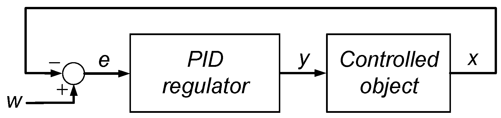
A typical application of the PID algorithm assumes that the PID regulator is included in a feedback loop (Figure 1).
The PID regulator is expected to tune the process variable x, which is not directly accessible, as close as possible to the setpoint w. This is accomplished through the appropriate adjustment of the manipulated variable y. The regulator evaluates the required value of the manipulated variable based on the error signal e = w − x, which is formed in the summing node.
In the classical form, the algorithm executed by the regulator is described by the formula presented in Equation (1) [44].
where
The result generated with the regulator consists of three components: proportional YP, integral YI, and derivative YD.
However, for practical applications, the basic formula, described by Equation (1), is often extended. Probably the most popular extension concerns the ideal derivative component, which is replaced by a high-pass filter function as described by Equation (3):
There are two reasons why this is performed:
- The ideal derivative function is not feasible in practical circuits;
- The gain of the ideal derivative function goes to infinity along with frequency, and, thus, it tends to amplify high-frequency noise, which can increase the output error (this problem was considered, e.g., in [45]). The gain of a high-pass filter transfer function goes with frequency to a constant value, so the influence of high-frequency components can be kept at a moderate level.
Another popular extension consists of introducing weighting coefficients b and c, which suppress the influence of the setpoint on the proportional and derivative components. The resulting formula is presented in Equation (4).
The output signal y, described by Equations (1) and (2), depends on the error signal , and, thus, it responds with equal intensity to changes in both the process variable x and the setpoint w. In practice, only rare changes in the setpoint are expected, but they are usually step changes. This leads to the overreaction of the regulator, which results from the contributions of the proportional and the derivative components. By introducing and appropriately tuning the b and c weighting coefficients, a smoother and more “bumpless” operation of the regulator can be achieved, when the setpoint is changed in the step mode. It prevents the unnecessary wear-out of the actuators.
The extended PID formula presented in Equation (4) will be the base for the solution presented in this paper.
3. Discretization of the PID Formula
Before a relationship described in the continuous time domain is implemented in a digital system, it needs to be discretized, i.e. converted to the discrete-time domain. To accomplish this, the backwards difference method shall be used, which, in fact, is the most popular approach. The discretization of a continuous-time formula using the backwards difference method is most conveniently carried out in the operator domain and consists of substituting for .
The most obvious and popular approach to the discretization of the PID formula consists of separately discretizing all three components contributing to the result, i.e., the proportional, integral, and derivative functions. The application of the foregoing approach to the formula described by Equation (4) leads to the following:
and
Converting to the time-domain yields to
and
Besides the integral component , the derivative component also depends on its previous samples. It means that the and values need to be stored somewhere in the system, and the , , and components have to be calculated separately. It is not a problem when the formulas are implemented in software. However, in the case of hardware implementations, it leads to an irregular, and less optimal structure.
However, a different approach is proposed in this paper, namely the one-shot discretization of the PID formula as a whole. By substituting for in Equation (4), the following formulations are obtained:
Both sides of the equation can be multiplied by to eliminate the denominators from the integral and derivative components:
The formula needs to be rearranged by grouping together the components depending on the W and X signals, respectively:
The next manipulations assume the grouping of components according to the negative powers of z:
Thus, can be derived:
The last transformation consists of converting the formula to the discrete-time domain:
The – coefficients depend on the regulator parameters KP, TI, TD, a, b, c, and the sampling period TS as follows:
According to Equation (18), the current sample of the regulator output signal y(n) can be calculated using current values of the process variable x and the setpoint w, as well as two preceding samples of x, w, and y.
Should the same method be applied to the basic PID formula shown in Equation (1), the regulator is reduced to a second-order IIR (Infinite Impulse Response) filter.
The PID formula described by Equation (18) is very regular. For a hardware designer, it offers many options to arrange hardware components that perform the relevant arithmetic operations. These options include parallel, serial, and mixed structures.
Two preceding samples of the regulator output y, the process variable x, and the setpoint w need to be stored in the system. However, this is more convenient than storing samples of the integral and derivative components. The y, x, and w signals are directly available either at the regulator inputs, or outputs, so they do not need to be calculated separately using dedicated hardware.
4. The Proposed Circuit Structure
As it was mentioned above, the regular form of Equation (18) offers a hardware designer plenty of freedom in designing the structure of the circuit for the calculation of the PID formula. One of the remarkable solutions is the parallel, tree-shaped structure presented in Figure 2. Typically, parallel structures are supposed to provide the fastest operation of a system.
The implementation of the structure presented in Figure 2 requires eight two-input multipliers and seven two-input adders. As the calculations need to be performed on floating-point numbers, it is expected that the implementation will consume a significant amount of logic resources.
Further on in this paper, the assumption shall be made that the floating-point operations will be handled by “ready-made” IP (Intellectual Property) cores shipped together with synthesis software, which will be used to design the whole system. IP cores of various types, in particular, IP cores performing arithmetic operations on floating-point numbers, became a standard utility available in CAD software supporting FPGA design, delivered by all key FPGA vendors [46,47,48]. IP cores developed by FPGA vendors are carefully optimized, based on expertise in details of device architectures. Although one’s own IP core can be independently developed, it is quite unlikely to obtain a solution that is more efficient in terms of both performance and cost.
Sample experiments were carried out to estimate the parameters of the assumed parallel structure. The tests were accomplished using the Quartus Prime software (version 22.1, Lite edition) from Intel, Santa Clara, CA, USA, and a Cyclone V (5CGTFD9E5F35C7 [49]) device. For a given frequency of 100 MHz, the implementation of a floating-point multiplier IP core (the “FP Functions Intel FPGA” core [46]) requires 2 onboard fixed-point multipliers and 242 LUT (Look-up Table) blocks. The latency estimated by the IP Core generator is 4 clock cycles. The implementation of a floating-point adder (again, the “FP Functions Intel FPGA” core) requires 873 LUTs, and the latency is 5 clock cycles. This means that the implementation of the parallel structure presented in Figure 2 would consume at least 6303 LUTs, and the expected latency would be at least 19 clock cycles, i.e., 190 ns. Latency, divided by the maximum clock frequency, constitutes the low limit on the sampling period, and, as a consequence, the limit for the maximum speed achievable for a regulator.
As it was mentioned before, a serialized approach shall be proposed further on in this paper, since it is much more efficient in terms of logic resource usage.
The proposed structure is presented in Figure 3. The circuit is fully synchronous, i.e., all parallel registers and the MultAdd block are synchronized via a common clock signal.
The heart of the circuit is the MultAdd block, which should be implemented as an IP Core capable of performing simultaneous multiplication and addition operations on floating-point numbers (see Equation (27)).
Other crucial elements are parallel registers, which are arranged in two rings, with eight registers in each. The registers in the upper ring (the “variable ring”) store current and preceding samples of the process variable x(n), x(n − 1), x(n − 2), the setpoint w(n), w(n − 1), w(n − 2), and the regulator output y(n − 1) and y(n − 2). The registers in the lower ring (the “parameter ring”) store the values of the coefficients.
The output q of the MultAdd block is routed back to the block input c. In this way, a structure is obtained that is capable of storing temporary results for further processing, i.e., a kind of cumulative adder.
A simplified block diagram, depicting the operation of the circuit, is presented in Figure 4. The calculations described by Equation (18) are performed sequentially, i.e., initially, the product is calculated; then, the content of the rings is shifted right; then, the product is calculated and added to , which is available at the MultAdd block output q after the first product is calculated. Upon the completion of these calculations, the data are shifted once again, and the product is calculated and added to the result of previous operations. Subsequently, the , , , , and products are calculated and added to the temporary sum. Upon the completion of eight shift-and-calculate operations, the new sample of the manipulated variable y(n) is available at the MultAdd block output. The value is stored in a parallel register to be available for reading using external circuitry, and the circuit is ready for calculating the next sample of y.
Before a new calculation cycle is started, samples of the process variable x, the setpoint w, and the regulator output y must be updated. This is accomplished through the incorporation of 2-to-1 multiplexers at appropriate positions into the “variable” register ring. The “Select” inputs of the multiplexers are controlled by the external Start signal. The Start signal should be activated for one clock cycle before the actual calculations begin. The activation of the Start signal allows for new data to be loaded to the registers that store x(n), w(n), and y(n − 1). The remaining data are shifted right, following the ring direction. In this way, the old value of the x(n) sample is transferred to the register storing x(n − 1), while x(n − 1) is transferred to x(n − 2), w(n) to w(n − 1), and so on.
Updating the coefficients is accomplished in a similar manner. The registers in the “parameter ring” are interlaced with 2-to-1 multiplexers, and the “Select” inputs of the multiplexers are controlled by the Start input. However, it is assumed that the values of the coefficients do not need to be updated every time a new calculation cycle is initiated.
When a set of new values for the coefficients is ready, they can be simultaneously transferred to the R_c0–R_c7 registers. The transfer should be triggered at the beginning of a new calculation cycle. This is accomplished by appropriately driving the En (Enable) inputs of the R_c0–R_c7 registers. Apart from the Shift signal, which will be explained later on, loading new data to the R_c0–R_c7 registers is enabled when the condition is true. Start and Par_Wr are circuit inputs (see Figure 3). The Start signal has to be activated to initiate a new calculation cycle. The Par_Wr signal should be activated every time a modification of the regulator parameters is required and a set of new, consistent data is available at the inputs. Updating the coefficients will be commented on in a more detailed way in Section 7.
The operation of the whole circuit is governed by the Control block. The internal structure of the Control block incorporates two counter-like circuits. The first of them is responsible for generating the Shift signal, which triggers the shift operation in both rings, i.e., transferring data from R_x(n) to R_x(n − 1), from R_x(n − 1) to R_x(n − 2), etc. in the “variable ring”, and from R_c5 to R_c6, from R_c6 to R_c7, etc. in the “parameter ring”.
Performing the multiply-and-add operation on floating-point numbers is a complex task, for which a number of clock cycles is required. Assuming that the MultAdd block generates a valid result after l clock cycles, the first counter-like circuit activates the Shift signal every l-th clock cycle.
The second counter-like circuit is responsible for counting the subsequent multiply-and-add operations. After eight multiply-and-add calculations followed by shift operations are completed, the counter triggers loading the result to the R_y(i) register, activates the Ready output, and blocks the operation of the whole circuit until a new calculation cycle is initiated by activating the Start input.
5. Implementation of the Proposed Circuit
The circuit presented in Figure 3 was implemented in the Quartus Prime, v. 22.1, Lite Edition software from Intel. The register blocks, the control unit, and the whole circuit structure were described in the Verilog language. The MultAdd block was implemented using the “FP Functions Intel FPGA” IP core [46] configured for the multiply-and-add operation. The single-precision floating-point (32-bit) number format was selected for calculations.
The IP core generates a valid result after a number of clock cycles (i.e., latency), which can be selected within a certain range during the core configuration. Setting the latency parameter influences the maximum clock frequency at which the core is able to run, and its cost, i.e., the amount of logic resources required to have it synthesized. In general, setting a low latency (e.g., l = 2) leads to solutions requiring fewer logic resources but running at lower frequencies. On the other hand, when high latency values are selected, the eventual solutions are more expensive, but a benefit in operation frequency is achieved. So, setting the right parameters for the IP core is a kind of trade-off between speed and cost.
For the solution presented in this paper, the latency l was set to 10. The IP core generator estimated the maximum clock frequency of 102 MHz and the cost at 2 multiplier blocks plus 1192 LUTs.
The evaluation of the formula presented in Equation (18) requires eight multiply-and-add operations. With such an assumption, it is clear that the actual calculations take 8 × l = 80 clock cycles. One additional clock cycle is necessary to transfer the result to the output register after the result is ready. So, the whole calculation cycle for generating one sample of the output signal takes 81 clock cycles.
The circuit was synthesized for a Cyclone V device (5CGTFD9E5F35C7 [49]), which is classified as a cost-efficient option for an FPGA designer. After the design was actually synthesized, it turned out that the estimation of both the maximum clock frequency and resource usage delivered by the IP core generator was too pessimistic. The static timing analyzer module of the Quartus Prime system estimated the maximum clock frequency at 157.1 MHz. Therefore, it could be estimated that the execution time TE, i.e., the time delay, which is required, before a valid result is available at the circuit output, is 81 × 1/157.1 = 516 ns.
A comparison of parameters obtained for the proposed solution against some other ones presented in the references is shown in Table 1. The terms “basic” and “extended”, in the column of the table labeled “PID formula”, refer to the “basic” and “extended” PID formulas described by Equations (1) and (4).
Most of the structures presented in the table require a number of clock cycles to calculate a valid result. Thus, the tE (i.e., “execution time”) parameter was introduced to enable the realistic assessment of the speed achievable for the proposed solutions. The “execution time” is equal to the number of clock cycles N required to complete the calculations, divided by the estimation for maximum clock frequency fMax provided by static timing analysis tools.
The TE parameter constitutes the low limit for the sampling period, which is achievable for a particular case.
While analyzing the results presented in the table, one should keep in mind that the comparison is somewhat blurred by the fact that the designs use different FPGA devices, which may differ in logic resources available onboard (e.g., the availability of multiplier/DSP blocks) and their properties. In particular, the Spartan 6, Cyclone V, and Zynq FPGAs contain LUT blocks with six inputs, and, thus, offer bigger logic capacity, than four-input LUTs contained in all the other devices. If synthesized for structures featuring only four-input LUTs, the solutions reported for these FPGAs would possibly require more resources.
The shortest execution times TE, along with the smallest resource usage, were reported by Sreenivasappa and Udaykumar [37]. Similar results were obtained by Dhanabalan et al. [25]. The actual calculations are carried out with combinatorial structures capable of generating the result in one clock cycle. However, the question remains open as to whether the accuracy and dynamic range provided by the 8-bit fixed-point number format is sufficient for a wider class of applications than the ones described in the papers.
Yuen Fong Chan and Moallem [38] experimented with two regulator structures operating on 16-bit fixed-point numbers. The first structure incorporated parallel multipliers and was capable of generating the result in one clock cycle. The second implementation used serial multipliers, for which a number of clock cycles was required to obtain a valid result.
Applying a floating-point format for number representation makes the circuit much more complex; therefore, the implemented solutions are slower and more demanding for logic resources.
The flexibility of FPGA devices allows for the easy manipulation of the lengths of the mantissa and the exponent components in the floating-point representation. A question is how such manipulations affect the quality of regulation, and what lengths are required to assure a stable and reliable process. The use of the standard, single-precision, 32-bit floating-point number format, with 8 bits assigned for the exponent, and 23 bits for the mantissa, is commonly accepted, at least in PLCs. Such an approach is believed to provide sufficient accuracy for the great majority of regulation tasks.
Yankai Xu et al. [42] used a number format that resembles the conventional floating-point concept but used a 5-bit exponent, and 16-bit mantissa.
The standard single-precision floating-point format was used by Ziębiński et al. [43], Dedania and Sang-Woo Jun [21], and in this study. Unfortunately, exact data concerning the usage of logic resources expressed in LUT blocks are not reported in [43]. Nevertheless, the results comparable to the register counts can be expected, i.e., thousands. However, to be honest, the solution implemented by Ziębiński et al. comprises not only the actual arithmetic unit calculating samples of the y(n) signal but also contains some additional circuitry responsible for updating the regulator parameters.
The authors decided to enhance the comparison with two other cases and to present results obtained for structures, which were not directly designed by a human but generated automatically by software tools, right from a description in a high-level programming language. The first one [50] was generated for fixed-point numbers and the second one [51] was for the floating-point case. The authors believe that these examples enable readers to develop a more general view of what is possible and feasible.
Research works carried out by Milik are focused on developing algorithms that make it possible to directly transfer functions described originally by a PLC program into hardware resources available in FPGA devices. The solution reported in [50] was one of the benchmarks used by the authors to verify the efficiency of their algorithms. The regulator structure was generated using software algorithms from a program developed in the IL (Instruction List) language. Some more examples following this approach can be found in [52].
The solution presented in [51] was prepared to demonstrate the possibilities of high-level synthesis tools from Xilinx, San Jose, CA, USA. It was generated by the Vivado HLS system from a description in the C language. The solution uses a moderate number of LUT blocks but at the expense of as many as 5 DSP48 blocks.
The comparison presented in Table 1 indicates that the structure proposed in this study is comparable with the other implementations operating on floating-point numbers when considering operation speed, while being significantly cheaper. It is also worth mentioning that the regulators described by Ziębiński et al. and Dedania and Sang-Woo Jun implemented the basic PID formula (Equation (1)), while the circuit proposed in this paper uses the extended form (Equation (4)).
6. Testing and Verification
The correctness of the proposed circuit structure and its proper operation were verified through a number of functional tests. The tests were carried out with the use of the Questa Intel Starter FPGA Edition-64 2021.2 simulator from Siemens, Munich, Germany.
A simple Verilog testbench was prepared to supply appropriate samples of the x(n) and w(n) signals to the circuit inputs and to collect samples of the output signal y(n). The open-loop configuration was tested, i.e., the regulator as a standalone block without the manipulated object, and not surrounded by the negative feedback loop (see Figure 1).
The operation of the circuit was simulated for unit-step excitations applied to the circuit inputs x and w. A unit-step response in the time domain contains full information concerning the dynamic properties of an object subjected to the analysis, being also much easier for generation by means of common simulation tools, as compared to any response in the frequency domain.
In total, 1000 samples of the output signal, being a response to the unit step supplied to the input, were recorded for various sets of regulator parameters KP, TI, TD, a, b, c, and TS.
To provide the relevant reference data, a simple program in the C++ language was written. The program implements the “obvious” approach, i.e., the PID formula with the proportional, integral, and derivative components discretized separately (Equations (9)–(12)). The program operates on double-precision (64-bit) floating-point numbers.
Samples of the y(n) signal, obtained from simulation in the Questa software (Questa Intel Starter FPGA Edition-64 2021.2), were compared against the reference data provided by the C++ program. The highest value of relative error, which was recorded for parameter sets containing only the P and PD components is 1.2 × 10⁻⁶. This is a result of the limited accuracy of single-precision floating-point number representation, which is estimated at ca. 6–7 significant digits.
Errors greater by an order of magnitude were, in general, recorded for parameter sets containing the integral component. The greatest value of the relative error recorded during experiments was 7.6 × 10⁻⁵. The errors resulting from the limited precision of the number format tend to build up in the integral component.
Nevertheless, similar effects can be expected in the analog counterparts, which suffer from the limited precision of analog components, e.g., offset voltage. These effects are highly reduced in the closed-loop configuration containing the negative feedback (see Figure 1).
Sample plots, showing a comparison of the data obtained from the simulation against the reference data generated by the C++ program, are presented in Figure 5. Figure 5a shows data obtained for a PD regulator with the following parameters: KP = 1, TI = ∞, TD = 1, a = 0.1, b = 1, c = 1, and TS = 1. Figure 5b presents data obtained for a PID regulator with KP = 0.5, TI = 0.75, TD = 0.2, a = 0.1, b = 0.62, c = 0, and TS = 0.1. The latter set of parameters was generated with the autotuner included in the TIA Portal software from Siemens for a popular S7-1200 PLC controlling a small DC drive. In both cases, the simulated circuit was excited by unit step signals with magnitudes of 0.1 and 1 applied, respectively, to the x and w inputs.
The analysis of the data obtained from the verification process, as described above, indicates that the circuit proposed in this study properly implements the digitalized version of the extended PID formula described by Equation (4).
7. A General Concept of the Entire Regulator Device
The circuit described in Section 4 can serve as the “execution unit”, i.e., the main part of an actual regulator. However, such a unit must be accompanied by some additional circuitry to make up a fully functional device. The proposed concept of the entire regulator is presented in Figure 6.
The “PID calculator” described in Section 4 operates on floating-point numbers. Samples of the process variable x need to be delivered to its inputs in the appropriate format. Similarly, samples of the manipulated variable y, calculated using the “PID calculator”, need to be converted and transferred to the regulator output. These operations should be accomplished with the “Input read and format conversion” and “Format conversion and output write” blocks.
The process variable x is expected to be an analog signal. Thus, the “Input read and format conversion” block should comprise in particular an A/D converter and circuitry that converts a fixed-point number, delivered by the A/D converter, to the floating-point format processed with the execution unit. Similarly, the “Format conversion and output write” block should contain a kind of D/A converter (e.g., circuitry generating a pulse-width modulation signal), and a circuit that converts the floating-point number calculated by the executive unit to a fixed-point representation, which is appropriate for D/A conversion.
If modifying the regulator parameters is a required function of the device, the circuit should contain a CPU/MCU core, responsible in particular for the conversion of the regulator parameters KP, TI, TD, a, b, c, and TS to the – coefficients suitable for the execution unit. During the typical operation of a PID regulator, the KP, TI, TD, a, b, c, and TS parameters are accessed and manipulated, rather than . This concerns both a human operator, and a high-level application software, e.g., an autotuner, which is capable of finding the best values of the regulator parameters for a particular object.
The coefficients are complex functions of KP, TI, TD, a, b, c, and TS, containing, in particular, the division operation (see Equations (19)–(26)). Implementing the conversion functions in hardware would be very expensive in terms of logic resource usage. On the other hand, a change in the PID regulator parameters is quite a rare case, if compared to cyclic and permanent calculations of new samples at the regulator output. Calculating new values of the coefficients is not a time-critical task, and it can be conveniently handled using software running on the CPU. Moreover, introducing a CPU core to the device structure facilitates the implementation of many additional useful functionalities, like handling user interface, network communication, self-diagnostic, or, in particular, autotuning algorithms.
The analysis of Equations (19)–(26) makes it possible to draw the conclusion that modifying even a single regulator parameter usually leads to changes in most of the coefficients. Thus, a possible update of the coefficients should always affect all of them. The need to modify a single coefficient separately is very unlikely.
To enable the smooth operation of the regulator, without the need to stop the regulation every time, when a parameter needs modification, the regulator structure should comprise a set of eight parallel registers that shall serve as the source of new data for the inputs (see Figure 3). The registers should be integrated with the CPU system, e.g., as parallel I/O ports. In that way, the CPU core will be able to access them freely, at moments convenient for the program the CPU is executing. When a consistent set of new values of the coefficients is ready to be accessed with the execution unit, the CPU can trigger parameter updates by activating the Par_Wr input together with the Start input (see Figure 3). It is important to change all the coefficients at once in order to prevent the unpredictable behavior of the regulator.
Another possible application of the circuit presented in Figure 3 consists of using it as a regulator, which is dedicated to a specific object (e.g., a DC–DC converter). In such a case, it is quite possible that the regulator parameters will not change during the whole lifecycle of the device. Thus, the set of regulator parameters can be calculated only once, before the circuit is actually synthesized, and the new values for the coefficients can be implemented as constants. In such a case, the CPU/MCU core is not required, and the components of the circuit presented in Figure 3, responsible for controlling the coefficient update, i.e., the input, together with the corresponding And functor, can be deleted.
Furthermore, in certain technologies, e.g., modern SRAM-based FPGA devices, it is possible to freely set the initial values of all memory elements. Should the regulator be implemented in such a device, the coefficients can be downloaded to the Reg_c0–Reg_c7 registers after reset, together with the device configuration, and the Mux_c0–Mux_c7 multiplexers can be eliminated as well.
Alternatively, the CPU can be substituted with an AI circuit, e.g., a neural network to be used for parameter tuning.
8. Conclusions
The paper proposes a new implementation of the PID algorithm in digital hardware. The proposed circuit implements the extended PID formula (Equation (4)), containing a non-ideal derivative component, as well as weighting coefficients in the proportional and derivative components, which enables reducing the influence of rapid changes in the setpoint to the regulator output.
The PID formula is discretized and converted to a form where samples of the output signal y depend on current values of the process variable x, the setpoint w, and two preceding samples of y, x, and w (Equation (18)). The evaluation of the results needs eight multiplication and seven addition operations. The final formula is very regular, which offers many options to a hardware designer to arrange hardware components necessary to perform the relevant arithmetic operations.
The implementation presented in the paper operates on standard, single-precision (32-bit) floating-point numbers. The proposed circuit structure is optimized for cost, i.e., the amount of logic resources required for implementation. It contains only one arithmetic block. The structure consists of three main parts: the MultAdd block, responsible for performing the actual calculations, and two sets of parallel registers arranged in two rings: the “variable ring” and the “parameter ring” (see Figure 3). The “variable ring” stores current and preceding samples of the y, x, and w variables, while the “parameter ring” contains a set of eight coefficients, which depend on the actual regulator parameters KP, TI, TD, a, b, c, and TS.
The calculations are accomplished in a sequential manner: the data in both rings are shifted and subsequently applied to the MultAdd block inputs, in which the partial and final results are actually evaluated.
The circuit was implemented in a Cyclone V FPGA device from Intel, using the Quartus Prime software (version 22.1, Lite edition). The MultAdd block was implemented as an IP core available in the tool. The validation of the circuit was carried out as a simulation in the Questa Sim simulator (Questa Intel Starter FPGA Edition-64 2021.2).
For the particular implementation, which is described in the paper, 81 clock cycles are required to evaluate one sample of the output signal. Since the maximum clock frequency was estimated using the static timing analysis tools at ca. 150 MHz, the delay, which is required, before a valid result is available at the circuit output, can be estimated at ca. 550 ns. So, the solution presented in the paper is comparable, in terms of speed, with other hardware implementations of the PID algorithm operating on standard single-precision floating-point numbers presented in the references, where the delay ranges from 215 ns to 1560 ns. The parameters offered by the solution disclosed in this paper should meet speed requirements demanded by the fastest control tasks reported in the literature, i.e., precise motion control, controlling the operation of voltage converters, or the stabilization of magnetic bearings, where sampling periods within the range of tens of microseconds are required.
However, the solution presented in the paper is much more efficient in the usage of logic resources. It uses 1173 LUT blocks, 1026 registers, and 1 DSP block, while most of the other structures require ca. 4000 LUT blocks and a similar number of registers. The solution presented herein is, thus, much cheaper, leaving more space in the FPGA for other functionalities, like CPU/MCU cores, or elements of artificial intelligence.
Should the modification of the regulator parameters be a mandatory function of the device, the circuit described in the paper should be included as the “execution unit” in a bigger system governed by a CPU/MCU core. Such a system can be conveniently implemented in an SoC (System-on-Chip), or SoPC (System-on-Programmable-Chip) device, i.e., a device, that, apart from the “FPGA fabric”, also contains a CPU core. Devices of this type are on offer by all main PLD vendors and are becoming more and more popular among designers.
Author Contributions
Conceptualization, J.K. and F.J.; methodology, J.K.; implementation, J.K.; software, F.J.; validation, J.K. and F.J.; formal analysis, F.J.; resources, J.K. and F.J.; writing—original draft preparation, J.K.; writing—review and editing, F.J.; supervision, J.K. All authors have read and agreed to the published version of the manuscript.
Funding
This work was supported by funding from the Ministry of Science and Higher Education for Statutory Activities of Digital Systems Division of the Silesian University of Technology in Gliwice (02/150/BK_24/0021).
Data Availability Statement
The raw data supporting the conclusions of this article will be made available by the authors upon request.
Conflicts of Interest
Author Filip Jokiel is an employee of the Cadence Design Systems company. The remaining authors declare that the research was conducted in the absence of any commercial or financial relationships that could be construed as a potential conflict of interest.
References
- Siemens AG. SIMATIC. Standard PID Control Manual; Documentation No. A5E00204510-02; Edition 03/2003; Siemens AG: Munich, Germany, 2003. [Google Scholar]
- Rockwell Automation. Estimated Logix 5000 Controller Instruction Execution Times. Reference Manual. Rockwell Automation Publication LOGIX-RM002B-EN-P—July 2019. Available online: https://www.google.com.hk/url?sa=t&source=web&rct=j&opi=89978449&url=https://literature.rockwellautomation.com/idc/groups/literature/documents/rm/logix-rm002_-en-p.pdf&ved=2ahUKEwjcv5CuycWFAxVvslYBHTlSD90QFnoECBgQAQ&usg=AOvVaw043BzUdJatbHjHWUBYEsad (accessed on 11 March 2024).
- Siemens, AG. SIMATIC S7-1200, S7-1500 PID Control. Function Manual; Documentation No. A5E35300227-AG; Edition 11/2023; Siemens AG: Munich, Germany, 2023. [Google Scholar]
- Mirac, B.; Kilic, A. Assessment of Several PID Controllers Applied to DC Motors. In Proceedings of the 5th International Symposium on Multidisciplinary Studies and Innovative Technologies, ISMSIT’2021, Ankara, Turkey, 21–23 October 2021. [Google Scholar]
- Zhang, M.; Guo, L.; He, C.; Bao, B.; Lu, Z. Design and implementation of control system for transport robot based on STM32 microcontroller. In Proceedings of the IEEE International Conference on Artificial Intelligence and Computer Applications, ICAICA’2021, Dalian, China, 28–30 June 2021. [Google Scholar]
- Zhao, C.; Hua, Z. Design of Motor Speed Control System Based on STM32 Microcontroller. In Proceedings of the IEEE International Conference on Computation, Big-Data and Engineering, ICCBE’2022, Yunlin, Taiwan, 27–29 May 2022. [Google Scholar]
- Huang, Y.; Chen, H.; Qin, L. Design of self-balancing vehicle based on cascade PID control system. In Proceedings of the 4th International Conference on Advances in Computer Technology, Information Science and Communications, CTISC’2022, Suzhou, China, 22–24 April 2022. [Google Scholar]
- Blachuta, M.; Bieda, R.; Grygiel, R. Sampling Rate and Performance of DC/AC Inverters with Digital PID Control—A Case Study. Energies 2021, 14, 5170. [Google Scholar] [CrossRef]
- Zhang, X. Research and design of a three-port DC-DC converter based on PID algorithm. In Proceedings of the IEEE 4th International Conference on Civil Aviation Safety and Information Technology, ICCASIT’2022, Dali, China, 2–14 October 2022. [Google Scholar]
- Ren, Z.; Tang, Z.; Wang, R. Research on key technologies of four-rotor UAV flight control system based on STM32 microcontroller. In Proceedings of the IEEE 6th International Conference on Information Systems and Computer Aided Education, ICISCAE’2023, Dalian, China, 23–25 September 2023. [Google Scholar]
- Chu, C.T.; Chang, Y.S.; Wang, Y.K. Ultra low power MSP432 calculation for PID-neural control in magnetic bearing system. In Proceedings of the 5th International Symposium on Next-Generation Electronics (ISNE), Hsinchu, Taiwan, 4–6 May 2016; pp. 1–2. [Google Scholar] [CrossRef]
- Zhou, C.; Zhang, Q.; Ezechias, D.D.; Gao, Y.; Deng, H.; Qu, S. A General Digital PID Controller Based on PWM for Buck Converter. In Proceedings of the 11th World Congress on Intelligent Control and Automation, Shenyang, China, 29 June 2014–4 July 2014. [Google Scholar]
- Guo, L. Implementation of Digital PID Controllers for DC-DC Converters using Digital Signal Processors. In Proceedings of the 2007 IEEE International Conference on Electro/Information Technology, Chicago, IL, USA, 17–20 May 2007. [Google Scholar]
- He, X.; Huang, C.; Li, Y.; Wang, H.; Lei, D.; Yao, M. An Adaptive Dimming System of High-Power LED Based on Fuzzy PID Control Algorithm for Machine Vision Lighting. In Proceedings of the IEEE 4th Information Technology, Networking, Electronic and Automation Control Conference, ITNEC’2020, Chongqing, China, 12–14 June 2020. [Google Scholar]
- Lei, Y.; Jin, X.; Zhou, Y. An Intelligent Control Strategy for Large Inertia Servo System. In Proceedings of the 5th International Conference on Smart Grid and Electrical Automation, ICSGEA’2020, Zhangjiajie, China, 13–14 June 2020. [Google Scholar]
- Noshadi, A.; Shi, J.; Poolton, S.; Lee, W.S.; Kalam, A. Comprehensive Experimental Study on the Stabilization of Active Magnetic Bearing System. In Proceedings of the Australasian Universities Power Engineering Conference, AUPEC’2014, Perth, Australia, 28 September–1 October 2014. [Google Scholar]
- Cheng, X.; Deng, S.; Cheng, B.-X.; Hu, Y.-F.; Wu, H.-C.; Zhou, R.-G. Design and Implementation of a Fault-Tolerant Magnetic Bearing Control System Combined With a Novel Fault-Diagnosis of Actuators. IEEE Access 2021, 9, 2454–2465. [Google Scholar] [CrossRef]
- Fan, X.; Li, Z.; Tao, Y.; Wang, Y.; Feng, S.; Li, W. Design of Adaptive Backstepping Control for Aircraft Generator Control System. In Proceedings of the IEEE International Conference on Predictive Control of Electrical Drives and Power Electronics, PRECEDE’2021, Jinan, China, 20–22 November 2021; pp. 92–97. [Google Scholar] [CrossRef]
- Kumar, V.; Nema, S.; Kumar, D.; Nema, R.K. DSP-Based PWM AC-DC Converter for DC voltage Regulation with Linear control Characteristics. In Proceedings of the IEEE 2nd International Conference on Electrical Power and Energy Systems, ICEPES’2021, MANIT, Bhopal, India, 10–11 December 2021. [Google Scholar]
- Chen, S.-C.; Hoai, H.-K. Studying an Adaptive Fuzzy PID Controller for PMSM with FOC based on MATLAB Embedded Coder. In Proceedings of the IEEE International Conference on Consumer Electronics–Taiwan, ICCE-TW’2019, Yilan, Taiwan, 20–22 May 2019. [Google Scholar]
- Dedania, R.; Jun, S.-W. Very Low Power High-Frequency Floating Point FPGA PID Controller. In Proceedings of the 12th International Symposium on Highly-Efficient Accelerators and Reconfigurable Technologies, HEART’22, HEART2022: International Symposium on Highly-Efficient Accelerators and Reconfigurable Technologies, Tsukuba, Japan, 9–10 June 2022; pp. 102–107. [Google Scholar] [CrossRef]
- Das, P.; Edavoor, P.J.; Raveendran, S.; Rahulkar, A.D. Design and Implementation of Computationally Efficient Architecture of PID based Motion Controller for Robotic Land Navigation System in FPGA. In Proceedings of the Conference on Information and Communication Technology, CICT’17, Gwalior, India, 3–5 November 2017. [Google Scholar]
- Miao, Z.; Yang, F.; Li, B.; Gu, K.; He, C. The Application of Feedforward PID Control Based on FPGA in Universal Testing Machine. In Proceedings of the 38th Chinese Control Conference, Guangzhou, China, 27–30 July 2019. [Google Scholar]
- Mie, S.; Okuyama, Y.; Saito, H. Simplified Quadcopter Simulation Model for Spike-based Hardware PID Controller using SystemC-AMS. In Proceedings of the IEEE 12th International Symposium on Embedded Multicore/Many-Core Systems-on-Chip, Hanoi, Vietnam, 12–14 September 2018. [Google Scholar]
- Dhanabalan, G.; Tamil Selvi, S.; Mahdal, M. Scan Time Reduction of PLCs by Dedicated Parallel-Execution Multiple PID Controllers Using an FPGA. Sensors 2022, 22, 4584. [Google Scholar] [CrossRef] [PubMed]
- Zeng, H.T.; Yuan, J. A Fuzzy Adaptive PID System of DC Brush Motor for Snake Arm Robot. In Proceedings of the 2nd International Conference on Electrical Engineering and Control Science IC2ECS’2022, Nanjing, China, 16–18 December 2022. [Google Scholar]
- Cui, L.; Misdih, M. Adaptive Hierarchical Optimization of Sculpture 3D Printing Based on Fuzzy PID Algorithm. In Proceedings of the International Conference on Mechatronics, IoT and Industrial Informatics ICMIII’2023, Melbourne, Australia, 9–11 June 2023. [Google Scholar]
- Liu, J.; Pei, D.; Liu, M.; Sun, H. FPGA Implementation of Family Service Robot based on Neural Network PID Motion Control System. In Proceedings of the International Conference on Electronic Engineering and Informatics EEI’2019, Nanjing, China, 8–10 November 2019. [Google Scholar]
- Hassan, R.F.; Ajel, A.R.; Abbas, S.J.; Humaidi, A.J. FPGA based HIL co-simulation of 2DOF-PID controller tuned by PSO optimization algorithm. ICIC Express Lett. 2022, 16, 12. [Google Scholar]
- Sung, G.-M.; Chiang, P.-Y.; Tsai, Y.-Y. Predictive Direct Torque Control ASIC with Fuzzy Voltage Vector Control and Neural Network PID Speed Controller. In Proceedings of the IEEE International Future Energy Electronics Conference IFEEC’2021, Taipei, Taiwan, 16–19 November 2021. [Google Scholar] [CrossRef]
- Wang, J.; Li, M.; Jiang, W.; Huang, Y.; Lin, R. A Design of FPGA-Based Neural Network PID Controller for Motion Control System. Sensors 2022, 22, 889. [Google Scholar] [CrossRef] [PubMed]
- Lee, K.; Kim, Y. Design and Analysis of Digital PID Controller in MCU and FPGA. In Proceedings of the International SoC Design Conference ISOCC 2018, Daegu, Republic of Korea, 12–15 November 2018. [Google Scholar]
- Ngo, H.Q.T.; Nguyen, H.D.; Truong, Q.V. A design of PID Controller Using FPGA-Realization for Motion Control Systems. In Proceedings of the International Conference on Advanced Computing and Application ACOMP’2020, Quy Nhon, Vietnam, 25–27 November 2020. [Google Scholar]
- Rusia, P.; Bhongade, S. Design and Implementation of Digital PID Controller using FPGA for Precision Temperature Control. In Proceedings of the 6th IEEE Power India International Conference PIICON’2014, Delhi, India, 5–7 December 2014. [Google Scholar]
- Kocur, M.; Kozak, S.; Dvorscak, B. Design and Implementation of FPGA—Digital Based PID Controller. In Proceedings of the 15th International Carpathian Control Conference ICCC’2014, Velke Karlovice, Czech Republic, 28–30 May 2014. [Google Scholar]
- Trimeche, A.; Sakly, A.; Mtibaa, A.; Benrejeb, M. PID Controller Using FPGA Technology. In Advances in PID Control; Yurkevich, V.D., Ed.; InTech: Rijeka, Croatia, 2011; ISBN 978-953-307-267-8. [Google Scholar]
- Sreenivasappa, B.V.; Udaykumar, R.Y. Design and Implementation of FPGA Based Low Power Digital PID Controllers. In Proceedings of the Fourth International Conference on Industrial and Information Systems, ICIIS 2009, Peradeniya, Sri Lanka, 28–31 December 2009. [Google Scholar]
- Chan, Y.F.; Moallem, M.; Wang, W. Design and Implementation of Modular FPGA-Based PID Controllers. IEEE Trans. Ind. Electron. 2007, 54, 1898–1906. [Google Scholar] [CrossRef]
- Wadgaonkar, J.; Bhole, K.; Singh, P. Floating Point FPGA Architecture of PID Controller. In Proceedings of the International Conference on Industrial Instrumentation and Control ICIC’2015, Pune, India, 28–30 May 2015. [Google Scholar]
- Zurita-Bustamante, E.W.; Linares-Flores, J.; Guzmán-Ramírez, E.; Sira-Ramírez, H. FPGA Implementation of PID Controller for the Stabilization of a DC-DC “Buck” Converter. In Frontiers in Advanced Control Systems; Ginalber Luiz de Oliveira Serra; InTech: Rijeka, Croatia, 2012; pp. 215–230. [Google Scholar]
- Alinezhad, P.; Ahmadi, A. FPGA Design and Implementation of Digital PID Controller based on floating point arithmetic. In Proceedings of the 8th Symposium on Advances in Science and Technology 8thSASTech, Mashhad, Iran, 20 November 2014. [Google Scholar]
- Xu, Y.; Shuang, K.; Jiang, S.; Wu, X. FPGA Implementation of a Best-precision Fixed-point Digital PID Controller. In Proceedings of the International Conference on Measuring Technology and Mechatronics Automation ICMTMA’2009, Zhangjiajie, China, 11–12 April 2009. [Google Scholar]
- Zębiński, A.; Glinianowicz, M.; Lachowski, G. Implementacja regulatora PID w strukturze FPGA. Pomiary Autom. Kontrola PAK 2008, 54, 523–525. (In Polish) [Google Scholar]
- Visioli, A. Practical PID Control; Springer: London, UK, 2006. [Google Scholar]
- Liang, Y.; Liu, X. A Method for Improving Transient Response of the Source Measure Unit Based on PID+LPF Controller. In Proceedings of the IEEE 3rd International Conference on Power, Electronics and Computer Applications (ICPECA), Shenyang, China, 29–31 January 2023; pp. 748–751. [Google Scholar] [CrossRef]
- Intel Corporation. Floating-Point IP Cores User Guide; Documentation No. UG-01058, 2023.05.05; Intel Corporation: Santa Clara, CA, USA, 2023. [Google Scholar]
- AMD Corporation. Floating-Point Operator v7.1, LogiCORE IP Product Guide; Documentation No. PG060; AMD Corporation: Santa Clara, CA, USA, 2020. [Google Scholar]
- Lattice Semiconductor. DFPAU: Floating Point Arithmetic Unit. Available online: https://www.latticesemi.com/products/designsoftwareandip/intellectualproperty/ipcore/dcdcores/dfpau (accessed on 17 March 2024).
- Intel Corporation. Cyclone® V Device Handbook; Documentation No. CV-5V2, 2023.10.18; Intel Corporation: Santa Clara, CA, USA, 2023. [Google Scholar]
- Milik, A.; Hrynkiewicz, E. Hardware Mapping Strategies of PLC Programs in FPGAs. In Proceedings of the 15th IFAC Conference on Programmable Devices and Embedded Systems PDeS 2018, Ostrava, Czech Republic, 23–25 May 2018. [Google Scholar] [CrossRef]
- Bagni, D.; Mackay, D. Floating-Point PID Controller Design with Vivado HLS and System Generator for DSP; Xilinx Application Note XAPP1163 (v1.0). January 23, 2013. Available online: https://www.semanticscholar.org/paper/Floating-Point-PID-Controller-Design-with-Vivado-Bagni-Mackay/d167958905b1ff4506e29c174b2168f71e617d1a (accessed on 28 February 2024).
- Milik, A. On hardware synthesis and implementation of PLC programs in FPGAs. Microprocess. Microsyst. 2016, 44, 2–16. [Google Scholar] [CrossRef]
Figure 1.
A structure of a typical control system containing a PID regulator in the feedback loop.

Figure 2.
A parallel implementation of the PID formula.

Figure 3.
The proposed structure of the circuit calculating the PID algorithm.

Figure 4.
A simplified block diagram, depicting the operation of the proposed circuit.

Figure 5.
Sample plots showing a response to a unit step of (a) a PD regulator; and (b) a PID regulator.
Figure 5.
Sample plots showing a response to a unit step of (a) a PD regulator; and (b) a PID regulator.

Figure 6.
A general structure of the proposed PID regulator device.


Table 1.
A comparison of parameters obtained for various implementations of a PID regulator in FPGA devices.
Table 1.
A comparison of parameters obtained for various implementations of a PID regulator in FPGA devices.
| Work | PID Formula | Number Format | FPGA Device | Logic Resources | fclk [MHz] | Clock Cycles | tE [ns] |
|---|---|---|---|---|---|---|---|
| Sreenivasappa, B. V.; Udaykumar, R. Y [37] | basic | Fixed-point, 8 bits | Cyclone I | 224 LUTs, 32 registers | 75 | 1 | 13 |
| Yuen Fong Chan; Moallem, M. [38] (parallel structure) | extended | Fixed-point, 16 bits | Spartan 2E | 1142 slices (2284 LUTs), 327 registers | 15 | 1 | 67 |
| Yuen Fong Chan; Moallem, M. [38] (serial structure) | extended | Fixed-point, 16 bits | Spartan 2E | 437 slices (874 LUTs), 406 registers | 47 | 17 | 361 |
| Milik, A., Hrynkiewicz, E. [50] | extended | Fixed-point, 32 bits | Spartan 6 | 271 LUTs, 442 registers, 2 DSP48 blocks | 231.5 | 18 | 78 |
| Yankai Xu; et al. [42] | extended | Floating-point (mantissa—16 bits, exponent—5 bits) | Cyclone I | 1377 Les (1377 LUTs, 1377 registers) | 50 | 30 | 600 |
| Ziębiński, A. et al. [43] | basic | Floating-point, 32 bits | Virtex 4 | 4457 registers, 83,695 equivalent logic gates | 190 | 41 | 215 |
| Ziębiński, A. et al. [43] | basic | Floating-point, 32 bits | Spartan 2E | 4482 registers, 83,799 equivalent logic gates | 76 | 41 | 539 |
| Dedania, R., Sang-Woo Jun [21] | basic | Floating-point, 32 bits | iCE40 UP5K | 3998 LUTs, 3998 registers, 3 DSP blocks | 26 | 41 | 1560 |
| Bagni, D., Mackay, D. [51] | extended | Floating-point, 32 bits | Zynq | 1770 LUTs, 870 registers, 5 DSP48 blocks | 116 | 37 | 320 |
| This work | extended | Floating-point, 32 bits | Cyclone V | 1173 LUTs (339 with more than 4 inputs), 1026 registers, 1 DSP block | 157 | 81 | 516 |
Disclaimer/Publisher’s Note: The statements, opinions and data contained in all publications are solely those of the individual author(s) and contributor(s) and not of MDPI and/or the editor(s). MDPI and/or the editor(s) disclaim responsibility for any injury to people or property resulting from any ideas, methods, instructions or products referred to in the content. |
© 2024 by the authors. Licensee MDPI, Basel, Switzerland. This article is an open access article distributed under the terms and conditions of the Creative Commons Attribution (CC BY) license (https://creativecommons.org/licenses/by/4.0/).
Share and Cite
MDPI and ACS Style
Kulisz, J.; Jokiel, F. A Hardware Implementation of the PID Algorithm Using Floating-Point Arithmetic. Electronics 2024, 13, 1598. https://doi.org/10.3390/electronics13081598
AMA Style
Kulisz J, Jokiel F. A Hardware Implementation of the PID Algorithm Using Floating-Point Arithmetic. Electronics. 2024; 13(8):1598. https://doi.org/10.3390/electronics13081598
Chicago/Turabian StyleKulisz, Józef, and Filip Jokiel. 2024. "A Hardware Implementation of the PID Algorithm Using Floating-Point Arithmetic" Electronics 13, no. 8: 1598. https://doi.org/10.3390/electronics13081598
Note that from the first issue of 2016, this journal uses article numbers instead of page numbers. See further details here.