Article

High Electron Confinement under High Electric Field in RF GaN-on-Silicon HEMTs

Institute of Electronics, Microelectronics and Nanotechnology (IEMN), UMR-CNRS 8520, 59652 Villeneuve d’Ascq, France
*
Author to whom correspondence should be addressed.
Electronics 2016, 5(1), 12; https://doi.org/10.3390/electronics5010012
Submission received: 28 December 2015 / Revised: 11 March 2016 / Accepted: 14 March 2016 / Published: 18 March 2016
(This article belongs to the Special Issue Microwave/ Millimeter-Wave Devices and MMICs)

Abstract

:
We report on AlN/GaN high electron mobility transistors grown on silicon substrate with highly optimized electron confinement under a high electric field. The fabricated short devices (sub-10-nm barrier thickness with a gate length of 120 nm) using gate-to-drain distances below 2 µm deliver a unique breakdown field close to 100 V/µm while offering high frequency performance. The low leakage current well below 1 µA/mm is achieved without using any gate dielectrics which typically degrade both the frequency performance and the device reliability. This achievement is mainly attributed to the optimization of material design and processing quality and paves the way for millimeter-wave devices operating at drain biases above 40 V, which would be only limited by the thermal dissipation.

Graphical Abstract

1. Introduction

As a consequence to the rapid development of Radio Frequency (RF) power electronics, wide bandgap materials have been introduced due to their potential in high output power density, high operation voltage and high input impedance. Gallium Nitride (GaN)-based RF power devices have made substantial progress in the last decade, which will enable new applications demanding higher output power and efficiency at higher frequencies, especially in the Ka band (26–40 GHz) and beyond, with the aim of replacing or complementing traveling wave tube amplifiers. Satellite and broadband wireless communications as well as advanced radars are only a few of the many applications that would greatly benefit from the increased reliability, reduced size and reduced noise of these solid state-based amplifiers. In order to achieve the goal of operating at mm-wave frequencies and beyond, new process technologies and device structures have to be developed. Indeed, the device dimensions, such as the gate-to-channel distance, the gate length or the gate-to-drain distance, need to be reduced in order to increase the frequency performance. However, GaN device downscaling is usually achieved at the expense of a much lower breakdown voltage as compared to devices with larger dimensions [1,2,3,4]. This is due to the significant increase of the leakage current in these highly scaled devices that can result from many parameters such as bulk defects, interface and surface traps, as well as a poor electron confinement due to the epilayer design or process-induced imperfections.
Recently, sub-10-nm ultrathin barrier GaN transistors have been proposed [5] in order to avoid gate recessing which is commonly used to reduce the gate-to-channel distance while shrinking the gate length but generally causes reliability issues due to plasma damage under the gate [6]. In this frame, we have demonstrated the possibility of preventing gate tunneling through highly scaled Aluminum Nitride (AlN) barrier thickness (below 5 nm) by showing an extremely low gate leakage current [7,8]. On top of the material quality, the in situ grown SiN cap layer has been a key feature for controlling the surface parasitic leakage current and achieving high performance [9,10,11], namely by preventing the strain relaxation of the barrier layer.
In this paper, we report on the high breakdown voltage in highly scaled GaN transistors grown on a silicon substrate, showing that all the above-mentioned issues can be overcome in these emerging types of devices.

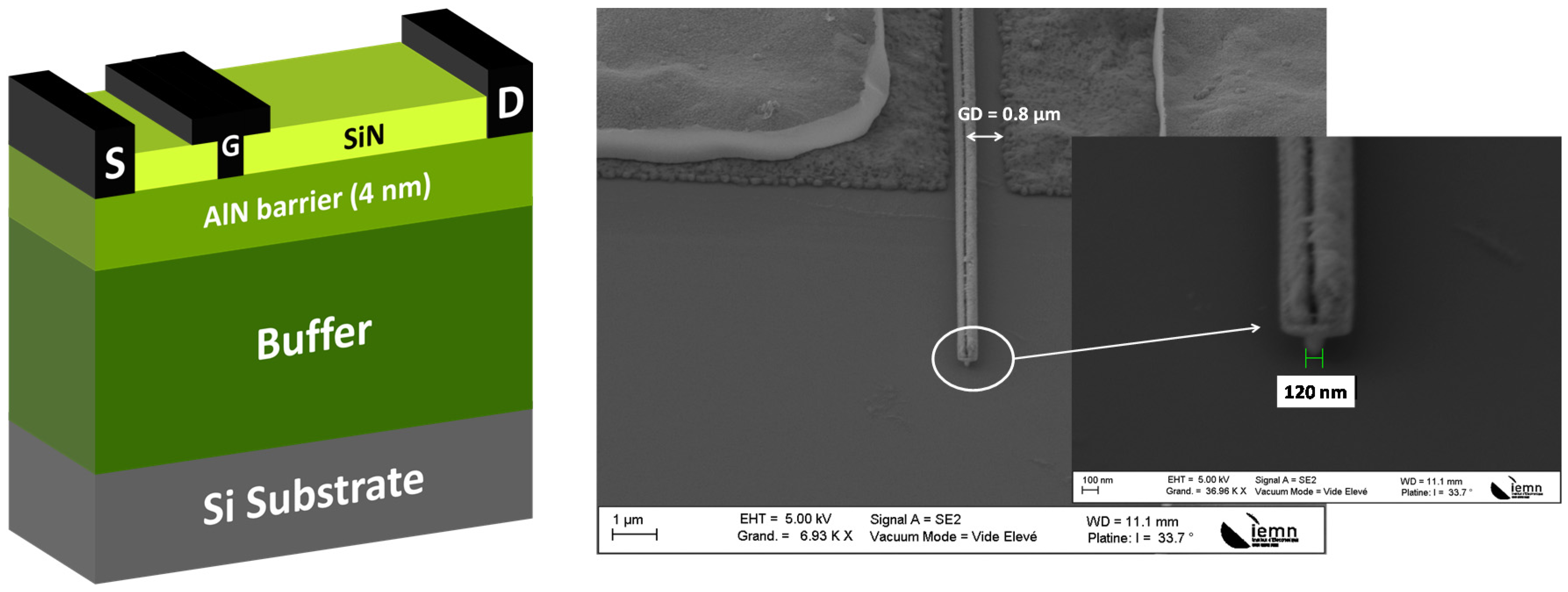
2. Experimental Section

The AlN/GaN heterostructures were grown by metal organic chemical vapor deposition (MOCVD) on a highly resistive 4 in Si (111) substrate. The High Electron Mobility Transistor (HEMT) structure consists of nucleation and transition layers, a 1.5-µm-thick buffer layer including undoped graded AlGaN back barrier layers, followed by a 100 nm GaN channel and a 4.0 nm ultrathin AlN barrier layer as well as a 5.0-nm-thick in situ Si3N4 cap layer (Figure 1). The in situ SiN layer is used both as early passivation as well as to prevent strain relaxation [12]. Room-temperature Hall measurements showed a high electron sheet concentration of 1.5 × 1013 cm−2 with a mobility of 1250 cm2/Vs in the heterostructure. Sheet resistance (Rsh) measurements revealed a high uniformity over the 4 in wafers with Rsh = 310 Ω/δ ± 3% in the HEMT structure. A Ti/Al/Ni/Au metal stack annealed at 875 °C has been used to form the ohmic contacts directly on top of the AlN barrier layer by etching the in situ Si3N4 layer. Device isolation was achieved by nitrogen implantation. Ohmic contact resistance (Rc) extracted from linear transmission line model (TLM) structures was 0.35 Ω mm. Then, a 120 nm Ni/Au T-gate was defined by e-beam lithography (Figure 1). The SiN underneath the gate was fully removed by SF6 plasma etching through the ebeam lithography. The gate-source was 0.3 µm and gate-drain spacings were 0.8 and 1.8 µm, respectively. The device width was 50 µm.

3. Results and Discussion

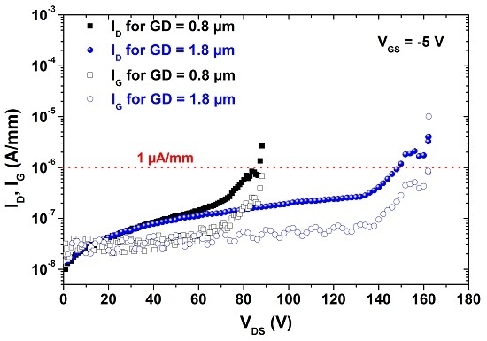
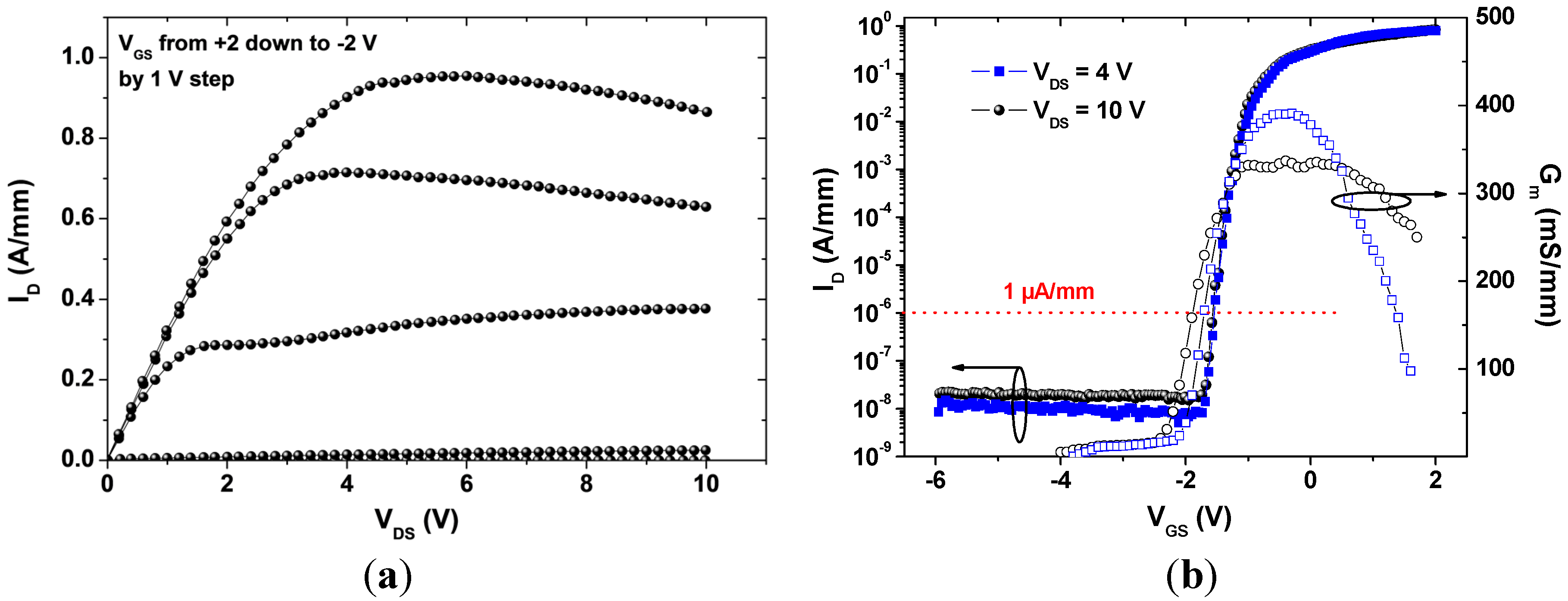
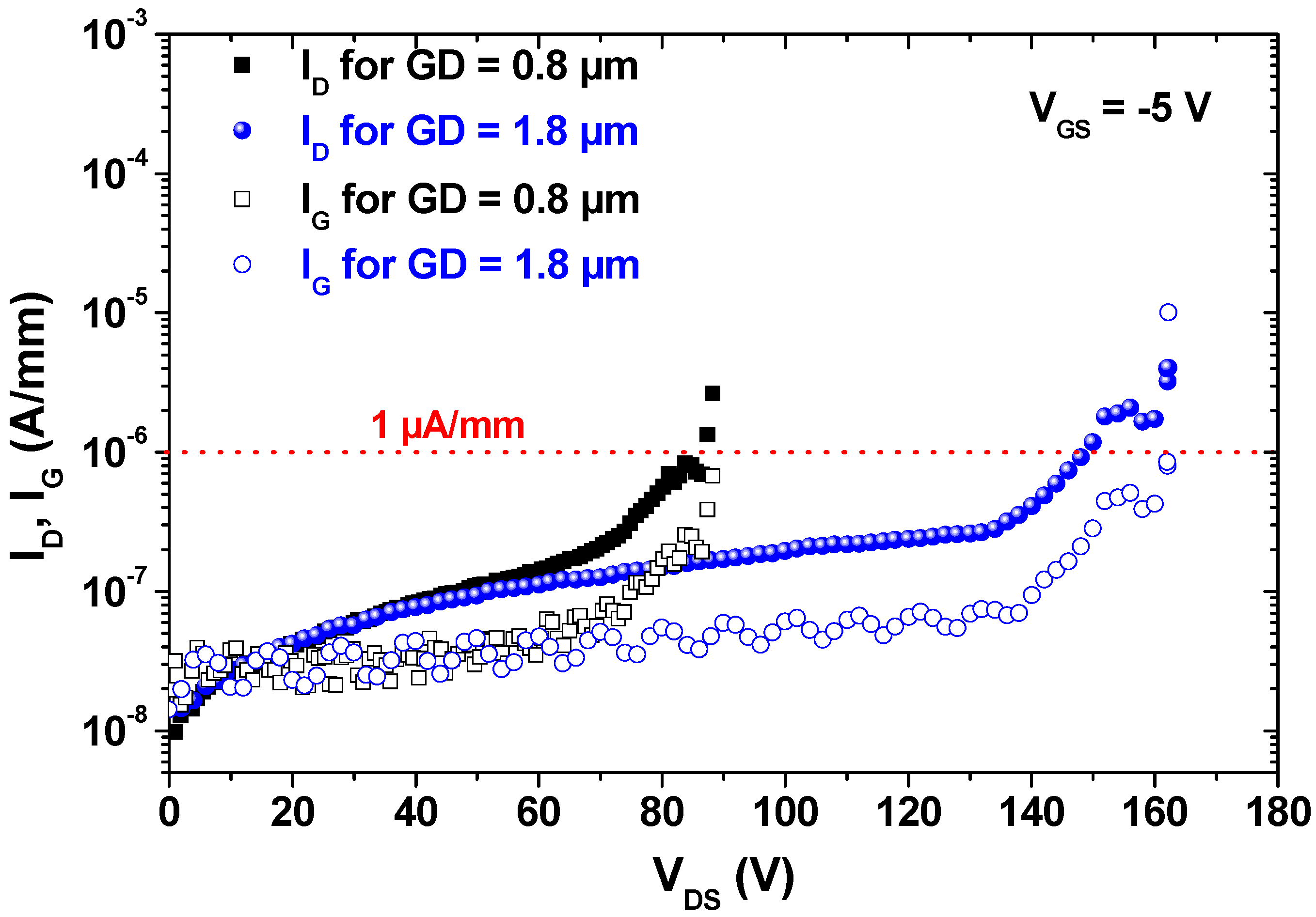
3.1. DC Characteristics

Typical output characteristics of 2 × 25 µm AlN/GaN-on-Si HEMT are shown in Figure 2a. The maximum DC current density at VGS = +2 V is about 1 A/mm with a peak extrinsic transconductance of 390 mS/mm at VDS = 4 V. In Figure 2b, the semi-log scale corresponding transfer characteristics at VDS = 4 and 10 V are plotted. It can be noticed that the transconductance decreases as a function of the drain bias due to the self-heating effect. In spite of a deep sub-micrometer gate length as well as short gate-drain distances and an ultrathin barrier layer, generating an extremely high electric field, a sub-threshold drain leakage current well below 1 µA/mm is reproducibly observed (within the range of several tenths of nA/mm) with no shift of the threshold voltage nor an increase of the leakage current as a function of VDS. This clearly shows an optimum electron confinement combined with high material quality and controlled surface parasitic leakage current.
The benefit of this configuration, enabling us to prevent both short-channel effects and the electron injection into the buffer layers under high electric field, is absolutely obvious in the sub-threshold region and is consequently reflected in the three-terminal breakdown voltage of these devices. Figure 3 indeed shows the off-state characteristics at VGS = −5 V of devices with a gate-to-drain distance of 0.8 and 1.8 µm. It can be noticed that an extremely low leakage current below 100 nA/mm is observed up to a high bias, yielding outstanding three-terminal breakdown voltages defined at 1 µA/mm of about 80 V and 160 V, respectively. This translates to a breakdown field ranging from 90 to 100 V/µm, which is favorably comparable to typical reported values in the literature for such short RF devices, especially in terms of leakage current level [13].

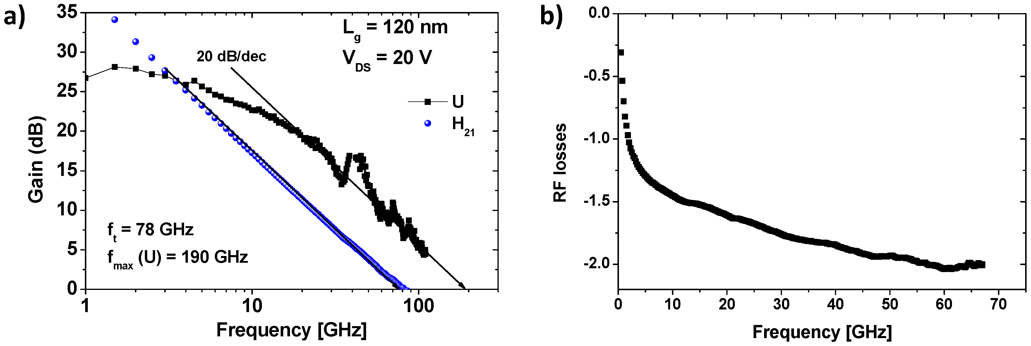
3.2. RF Characteristics

The S-parameters of a 0.12 × 50 µm2 AlN/GaN-on-Si HEMT were measured from 1 to 110 GHz. A current gain extrinsic cut-off frequency fT = 78 GHz and a maximum oscillation frequency fmax = 190 GHz (shown in Figure 4a) have been extrapolated from the current gain H21 and the unilateral power gain (U) at VDS = 20 V. The strong reduction of the short-channel effects by using a short gate-to-channel distance combined with high electron mobility in the two-dimensional electron gas (2DEG) explains the excellent power gain close to 200 GHz. It has to be pointed out that these frequency performances have been achieved despite non-optimized high RF losses of about 2 dB/mm as can be seen in Figure 4b. The RF losses extracted from transmission lines reflect a parasitic conduction at the buffer/Si substrate interface due to the intermixing between the GaN buffer layer and the Si substrate [14].
Further reduction of the contact resistances as well as the RF losses should result in an increase of the extrinsic transconductance and a significant improvement of the frequency performance. The use of sub-100-nm gate lengths in the AlN/GaN DHFET should therefore pave the way for higher frequency operation of GaN-based devices grown on highly resistive Si substrate combined with high power (e.g., high current density and high voltage).

4. Conclusions

We have developed high frequency AlN/GaN HEMTs grown on silicon substrate delivering an outstanding breakdown field close to 100 V/µm while using highly scaled dimensions such as sub-10-nm barrier thickness, 120 nm gate length and gate-to-drain distances below 2 µm. This achievement is mainly attributed to the optimization of both material design and processing quality enabling high electron confinement under a high electric field. These data show that millimeter-wave GaN devices operating in the Ka band and above can operate at unique drain biases above 40 V.

Acknowledgments

This work was supported by French Defense Procurement Agency (DGA) under the National Research project (ANR-13-ASTR-0022: CROCUS project), the French RENATECH network as well as the company EpiGaN for material delivery.

Author Contributions

All authors have participated to the design, the fabrication and the electrical characterization of the presented devices.

Conflicts of Interest

The authors declare no conflict of interest.

References

  1. Shinohara, K.; Regan, D.; Corrion, A.; Brown, D.; Burnham, S.; Willadsen, P.J.; Alvarado-Rodriguez, I.; Cunningham, M.; Butler, C.; Schmitz, A.; et al. Deeply-Scaled Self-Aligned-Gate GaN DH-HEMTs with Ultrahigh Cutoff Frequency. In Proceedings of the IEEE International Electron Devices Meeting (IEDM), Washington, DC, USA, 5–7 December 2011; Volume 19, pp. 1–4.
  2. Shinohara, K.; Regan, D.C.; Tang, Y.; Corrion, A.L.; Brown, D.F.; Wong, J.C.; Robinson, J.F.; Fung, H.H.; Schmitz, A.; Oh, T.C.; et al. Scaling of GaN HEMTs and Schottky Diodes for Submillimeter-Wave MMIC Applications. IEEE Trans. Electron Devices 2013, 60, 2982–2996. [Google Scholar] [CrossRef]
  3. Tirelli, S.; Marti, D.; Sun, H.; Alt, A.R.; Carlin, J.-F.; Grandjean, N.; Bolognesi, C.R. Fully Passivated AlInN/GaN HEMTs with fT/fMAX of 205/220 GHz. IEEE Electron Device Lett. 2011, 32, 1364–1366. [Google Scholar] [CrossRef]
  4. Yue, Y.; Hu, Z.; Guo, J.; Sensale-Rodriguez, B.; Li, G.; Wang, R.; Faria, F.; Song, B.; Gao, X.; Guo, S.; et al. Ultrascaled InAlN/GaN High Electron Mobility Transistors with Cutoff Frequency of 400 GHz. Jpn. J. Appl. Phys. 2013, 52, 08JN14. [Google Scholar] [CrossRef]
  5. Zimmermann, T.; Deen, D.; Cao, Y.; Simon, J.; Fay, P.; Jena, D.; Xing, H.G. AlN/GaN Insulated-Gate HEMTs with 2.3 A/mm Output Current and 480 mS/mm Transconductance. IEEE Electron Device Lett. 2008, 29, 661–664. [Google Scholar] [CrossRef]
  6. Meneghesso, G.; Meneghini, M.; Bisi, D.; Rossetto, I.; Wu, T.; van Hove, M.; Marcon, D.; Stoffels, S.; Decoutere, S.; Zanoni, E. Trapping and reliability issues in GaN-based MIS HEMTs with partially recessed gate. Microelectron. Reliab. 2015, in press. [Google Scholar] [CrossRef]
  7. Medjdoub, F.; Zegaoui, M.; Rolland, N.; Rolland, P.A. Demonstration of low leakage current and high polarization in ultrathin AlN/GaN high electron mobility transistors grown on silicon substrate. Appl. Phys. Lett. 2011, 98, 223502. [Google Scholar] [CrossRef]
  8. Cheng, K.; Degroote, S.; Leys, M.; Medjdoub, F.; Derluyn, J.; Sijmus, B.; Germain, M.; Borghs, G. AlN/GaN heterostructures grown by metal organic vapor phase epitaxy with in situ Si3N4 passivation. J. Crystal Growth 2011, 315, 204–207. [Google Scholar] [CrossRef]
  9. Medjdoub, F.; Grimbert, B.; Ducatteau, D.; Rolland, N. Record combination of power-gain cut-off frequency and three-terminal breakdown voltage for GaN-on-silicon devices. Appl. Phys. Express 2013, 6, 044001. [Google Scholar] [CrossRef]
  10. Medjdoub, F.; Zegaoui, M.; Grimbert, B.; Rolland, N.; Rolland, P.A. Effects of AlGaN Back Barrier on AlN/GaN-on-Silicon High-Electron-Mobility Transistors. Appl. Phys. Express 2011, 4, 124101. [Google Scholar] [CrossRef]
  11. Medjdoub, F.; Zegaoui, M.; Waldhoff, N.; Grimbert, B.; Rolland, N.; Rolland, P.A. Above 600 mS/mm transconductance with 2.3 A/mm drain current density AlN/GaN high-electron-mobility transistors grown on silicon. Appl. Phys. Express 2011, 4, 064106. [Google Scholar] [CrossRef]
  12. Derluyn, J.; Boeykens, S.; Cheng, K.; Vandersmissen, R.; Das, J.; Ruythooren, W.; Degroote, S.; Leys, M.R.; Germain, M.; Borghs, G. Improvement of AlGaN/GaN high electron mobility transistor structures by in situ deposition of a Si3N4 surface layer. Appl. Phys. Lett. 2005, 98, 054501. [Google Scholar]
  13. Murase, Y.; Asano, K.; Takenaka, I.; Ando, Y.; Takahashi, H.; Sasaoka, C. T-Shaped Gate GaN HFETs on Si with Improved Breakdown Voltage and fMAX. IEEE Electron Device Lett. 2014, 35, 524–526. [Google Scholar] [CrossRef]
  14. Hoshi, S.; Itoh, M.; Marui, T.; Okita, H.; Morino, Y.; Tamai, I.; Toda, F.; Seki, S.; Egawa, T. 12.88W/mm GaN High Electron Mobility Transistor on Silicon Substrate for High Voltage Operation. Appl. Phys. Express 2009, 2, 061001. [Google Scholar] [CrossRef]
Figure 1. Cross-section of the fabricated AlN/GaN-on-Si HEMTs (left) and SEM images of the 120 nm gate technology (right).
Electronics 05 00012 g001
Figure 2. (a) DC output ID-VDS characteristics of a 2 × 25 µm AlN/GaN-on-Si HEMT. VGS swept from −2 up to +2 V in 1 V steps; (b) Transfer characteristics of the 2 × 25 µm AlN/GaN-on-Si HEMT at various VDS (4 and 10 V) using LG = 0.12 µm.
Electronics 05 00012 g002
Figure 3. Off-state characteristics and gate leakage current at VGS = −5 V of the 2 × 25 µm AlN/GaN-on-Si HEMTs for gate-drain distances of 0.8 µm (black squares) and 1.8 µm (blue circles).
Electronics 05 00012 g003
Figure 4. (a) RF performance of the 0.12 × 50 µm2 AlN/GaN HEMT on silicon substrate at VDS = 20 V; (b) RF losses extracted from transmission lines up to 67 GHz.
Electronics 05 00012 g004

