Exploring the Limits of Floating-Point Resolution for Hardware-In-the-Loop Implemented with FPGAs


1
HCTLab Research Group, Universidad Autonoma de Madrid, 28049 Madrid, Spain
2
Facultad de Ciencias Exactas, Universidad Nacional del Centro de la Provincia de Buenos Aires, Tandil B7001BBO, Argentina
3
Faculty of Engineering, FASTA University, Mar del Plata B7600, Argentina
*
Author to whom correspondence should be addressed.
Electronics 2018, 7(10), 219; https://doi.org/10.3390/electronics7100219
Submission received: 7 September 2018
/
Revised: 24 September 2018
/
Accepted: 26 September 2018
/
Published: 27 September 2018
(This article belongs to the Special Issue Applications of Power Electronics)
Abstract
:As the performance of digital devices is improving, Hardware-In-the-Loop (HIL) techniques are being increasingly used. HIL systems are frequently implemented using FPGAs (Field Programmable Gate Array) as they allow faster calculations and therefore smaller simulation steps. As the simulation step is reduced, the incremental values for the state variables are reduced proportionally, increasing the difference between the current value of the state variable and its increments. This difference can lead to numerical resolution issues when both magnitudes cannot be stored simultaneously in the state variable. FPGA-based HIL systems generally use 32-bit floating-point due to hardware and timing restrictions but they may suffer from these resolution problems. This paper explores the limits of 32-bit floating-point arithmetics in the context of hardware-in-the-loop systems, and how a larger format can be used to avoid resolution problems. The consequences in terms of hardware resources and running frequency are also explored. Although the conclusions reached in this work can be applied to any digital device, they can be directly used in the field of FPGAs, where the designer can easily use custom floating-point arithmetics.
1. Introduction
Digital control for power converters has been growing during the past two decades [1,2,3,4,5]. Despite all the advantages of digital control, the debugging process of this type of control is more complex because the power converter is an analog system while the control is digital. Hardware-in-the-loop (HIL) is a technique that consists in the hardware implementation of mathematical models that represent a real system. HIL simulation presents numerous advantages such as having a safe environment to test controllers, allowing the use of the controller in its final implementation, even before building the real plant to be controlled. HIL techniques are being increasingly implemented using computers [6,7,8,9,10,11] and also digital devices like FPGAs (Field Programmable Gate Array) [12,13,14,15,16,17]. The latter make it possible to perform complex calculations faster. Thus, it is not surprising that several companies have released commercial HIL products [18,19,20].
Arithmetics used in HIL systems have a noteworthy impact in speed, hardware resources needed for the model, the complexity to design the model, and the accuracy of the system. Fixed-point arithmetics provide optimized operations in terms of area and speed. In [21], a comparison between fixed-point and floating-point arithmetics, in the context of FPGA-based HIL systems, was presented. Results showed that floating-point required ten times as many logic resources as well as it ran 10 times slower than fixed-point. For that reason, many HIL systems are based on fixed-point arithmetics when there are hard temporal restrictions [22,23,24,25,26].
The main drawback of fixed-point is that the implementation is more complex because the designer has to define the number of bits of the integer and fractional parts. Thus, the maximum representable value and the required resolution need to be calculated for every signal. However, in floating-point arithmetics, the designer does not take this definition into consideration, as an IEEE-754 single-precision floating-point number can store values up to , and the resolution is optimized in every calculation. This is accomplished by the floating-point libraries which automatically adapt the point location through the exponent field. Because of this remarkable advantage of floating-point, most HIL models actually use floating-point arithmetics [9,27,28], including commercial implementations [18,19,20].
Floating-point arithmetics for FPGAs were not viable in the past as there were no support libraries, and all the logic had to be implemented by the designer. However, with the release of floating-point support libraries, such as float_pkg of the VHDL-2008 Standard, it is easy to include floating-point arithmetics in a VHDL design. Lucia et al. [27] presented one of the first examples of a HIL model using floating-point in an FPGA.
In the literature not many cases of floating-point numerical issues for HIL systems have been reported, as the earliest purposes of HIL was to simulate complex systems with relatively low natural frequencies and integration steps of tens or hundreds of microseconds. With the advances in FPGAs, HIL technique started to be used for new applications, such as power electronics. Firstly, it was applied to converter models with low switching frequencies (kHz or tens of kHz). However, to simulate converters with medium to high switching frequency (hundreds of kHz or MHz), the integration step should be reduced accordingly and the system may present numerical problems, and as a result, obtain wrong simulations. The numerical issues are not related to overflows, as the exponent is automatically adapted. The problem is that, as the integration step is reduced, the increments of every step are smaller, and resolution issues may arise.
This paper explores the limits of floating-point arithmetics for HIL systems, and how to predict the floating-point format needed for accurate simulations. It explores not only the standard formats but also custom formats that can be used thanks to the VHDL-2008 standard libraries or any other libraries.
The rest of the paper is organized as follows. Section 2 shows the application example to illustrate the resolution problems for floating-point HIL simulations. Section 3 explains where the limits for single precision floating-point arithmetics are and how many bits would be necessary to increase the accuracy if needed. Section 4 and Section 5 show the experimental and synthesis results respectively. Finally, Section 6 gives the conclusions.
2. Application Example
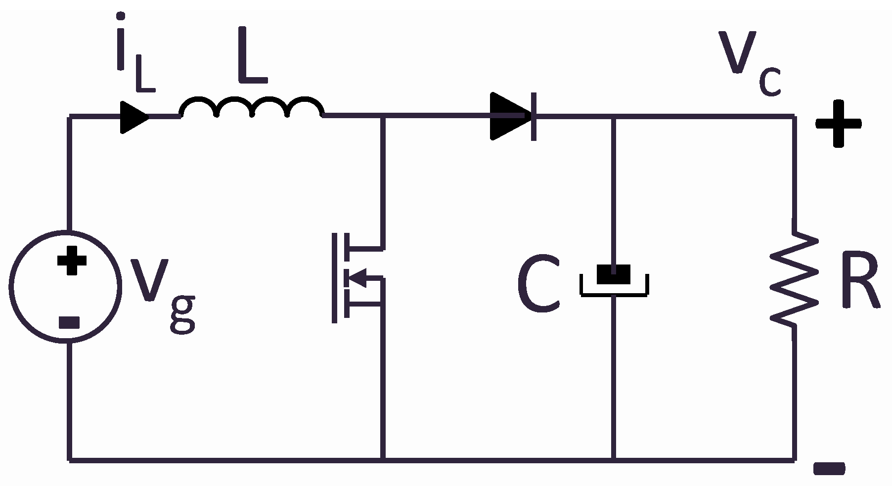
In this paper a PFC (Power Factor Correction) boost converter is used as an application example. The PFC technique allows regulating the output voltage while reducing the input current harmonics, so the converter behaves as a resistor emulator to the mains. The schematic of a boost converter is shown in Figure 1, excluding the previous diode bridge for ac/dc operation. The parameters of this plant are shown in Table 1. This boost configuration is proposed in an Infineon Design Note [29].
The converter can be modeled using the state variables of the system: the inductor current and the capacitor voltage. Therefore, both variables should be updated every simulation step.
The behavior of the inductor and the capacitor can be described using the following equations:
These equations can be discretized using different numerical methods but the simplest method to be used is explicit Euler [30]. While this method presents several disadvantages such as greater local and global error and risk of instability, these problems are negligible whenever very small integration steps (below microseconds) are used, so it is frequently used for HIL systems in power electronics [13,31,32,33]. Therefore, the previous Equations (1) and (2) can be discretized and the state variables can be defined as:
where has been converted into , which is the simulation step, i.e. the time between two calculations of the model.
As can be seen in the previous equations, the state variables depend on the inductor voltage and the capacitor current. These values depend on the conduction state of the switch and the diode, so several states should be considered.
If the switch is closed, the inductor voltage is , while the capacitor current is . In this case, the state variables are defined as:
If the switch is open, the conduction state of the diode depends on the inductor current. If the current is positive, the diode is conducting (called CCM or Continuous Current Mode) and the inductor voltage is , while the capacitor current is , so the state variables are:
Finally, if the inductor is fully discharged, the diode stops conducting (called DCM or Discontinuous Current Mode), so the capacitor current is :
The explicit Euler approach has been chosen in order to simplify the equations and get minimum simulation step. As the proposed system is based on an FPGA, both equations (inductor current and capacitor voltage) can be evaluated and updated in parallel, simplifying the resolution of the system. This is an important advantage compared with software-based HIL systems, in which equations need to be solved sequentially, one after another. Therefore, parallelization is one of the main reasons for the acceleration obtained using FPGAs. Taking advantage of this, every time step (), all the state variables are updated. The accuracy of the system relies on the small value of the simulation step. However, a small time step implies tiny increments for the state variables, as both are proportional. This can lead to resolution issues as it is explained in the next section.
3. Numerical Resolution
As it was explained in the previous section, the model updates its state variables every simulation step. There is a relation between the simulation step and the switching frequency, because the model should be updated with enough intermediate steps inside a switching period. This update is necessary to detect accurately the state of the switch and the diode of the converter so, the smaller the switching period is, the smaller the simulation step should be. In other words, the relation between the switching period and the simulation step is the resolution of the duty cycle. Therefore, the simulation step, and then the increments for the state variables, should be quite small. As HIL systems were firstly applied to low switching frequency converters, numerical issues have not been thoroughly studied in the literature. However, as HIL systems are being used for higher frequency converters, resolution problems arise because the variables width is limited to be able to run the model in real-time [34].
Obtaining low numerical resolution leads to poor accuracy simulations or even an unpredictable simulation behavior. For example, if the system is in steady state and it suffers any small change in the input voltage or load, it is possible that the output voltage changes with the opposite sign rather than the expected one. Besides, the problem is difficult to detect because the system may be able to detect bigger changes in the input conditions, but not the smaller ones.
The optimal solution is to increase the variables width. However, if the width is increased, the calculations are more complex, more hardware resources must be used, and the combinational paths between the flip-flops inside the FPGA get longer. In conclusion, increasing the width leads to longer simulation steps, which have a negative impact on the accuracy of the simulation.
Taking all the previous considerations into account, a trade-off between the simulation step and resolution should be reached. The minimum number of bits can be estimated considering the relation between the maximum expected value of a variable x, , and the increment that should be added, [34]. Besides, some extra bits, n, should be included to store the increment value with more than 1 bit of resolution:
The first operation calculates the number of integer bits needed to store , that is, the exponent. The second gives the bits needed to store the increment. That second term may be negative, as the increment is usually below 0, indicating that fractional digits should be included. Therefore the subtraction calculates the number of bits needed for the significand field, as it has to store both the value of x and its increments simultaneously.
The maximum values of the state variables are easy to calculate because they are defined by the limits of the converter design. Regarding the increments, it is also easy if they are stable, e.g., in the case of a dc-dc converter in steady state, but otherwise further analysis must be done.
For a boost-based PFC configuration, which is the example of this paper, the minimum incremental values for the output capacitor voltage are reached when is similar to , as shown in Equations (4)–(6). Likewise, the minimum incremental values for the inductor current are reached when is near 0 (in the case of closed switch).
As the number of bits is limited, infinitesimal incremental values will not be properly computed, but the designer can estimate the number of bits that will be necessary to obtain accurate resolutions. In [34], a fixed-point based HIL model for a PFC converter was presented. In that article, the model presented high accuracy when it had enough bits to store the incremental values during 95% of the ac period. We have to take into account that the remaining 5% has a minimum impact on the overall simulation because during that time the increments are smaller than the rest of the time and, therefore, almost negligible.
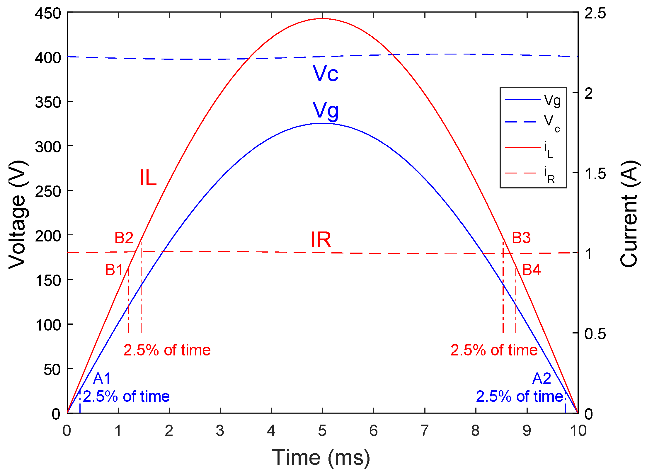
Following the aforementioned rule of 95%, and given the characteristics of the PFC converter proposed in Table 1 and the current and voltage waveforms from Figure 2, it is possible to calculate the minimum incremental values considered for the state variables. Figure 2 shows points A1 and A2 which correspond to the minimum considered input voltage. Likewise, points B1-4 correspond to the minimum considered difference between currents. Using these points, the minimum considered increments are as follows:
In the previous equations, a value of 50 ns was used as the simulation step (). With the results of the previous equations, it is possible to calculate the number of bits needed for both variables, which are included in Section 4.
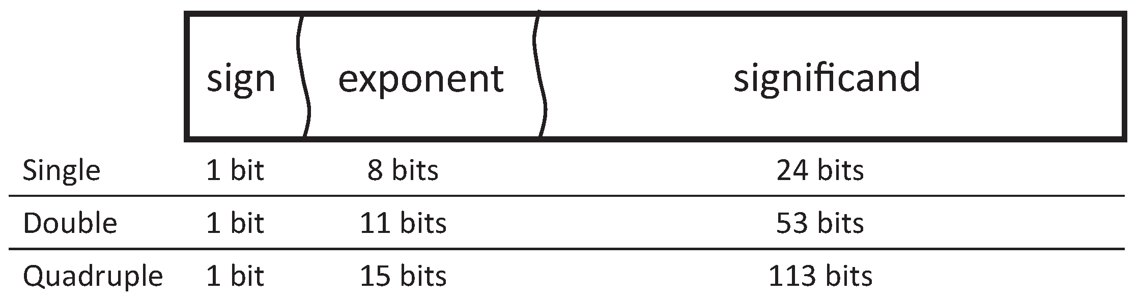
Once the required significand width is obtained, it is possible to estimate the needed floating-point format. IEEE-754 floating-point format [35] defines three binary-based floating-point formats with 32, 64, and 128 bits, also known as Single, Double, and Quadruple precision, respectively. In the field of FPGAs, most cases use single-precision floating-point, as the hardware cost of Double and Quadruple precision formats, in terms of area and speed, makes it inviable to use them.
Custom floating-point formats can be used in order to reach a trade-off between speed, area and numerical resolution. The floating-point formats include separated fields for the sign, exponent, and significand, as can be seen in Figure 3. The problem in power converter HIL models is not the number of exponent bits, as the magnitudes are not extremely big or small, but the number of bits of the significand. Therefore, only the significand field should be enlarged reaching the number of bits calculated using Equations (7) and (8).
In the case of VHDL, this custom floating-point format can be defined using the floating-point package included in the VHDL-2008 standard [36]. Using this package, the codification of Equations (4)–(6) is trivial, so the format of the model variables only has to be taken into account while declaring the signals.
4. Simulation Results
The previous section showed that the designer must reach a trade-off between speed, hardware resources, and accuracy. Therefore, the number of bits cannot be increased as desired. This section compares the accuracy of different floating-point formats regardless of speed and hardware resources.
It is important to note that the designed model has to be tested in open loop, without using any feedback from the control loop. If closed loop were used, the regulator would compensate the numerical errors of the model, so the whole system would probably get the desired current and voltage values at steady state. Simulations in open loop for power factor correction can be done using pre-calculated duty cycles for the PWM signal. This technique has been used previously in the literature because of its low cost, since it gets rid of the current sensor in the case of PFC converters [37,38,39]. Although using pre-calculated duty cycles also presents disadvantages, such as sensitivity to non-nominal conditions, it can be perfectly used to quantitatively measure the accuracy of the model, as any drift of the model will not be compensated, because it allows open-loop operation for PFC.
Table 2 presents the different experimental scenarios that have been tested, including different output loads, and cases starting at nominal steady state (400 V) and also with small capacitor voltage transients. In the case of the transients, the system will move slowly towards the nominal state following the dynamics of the chosen PFC/Boost converter, as the duty cycles are not modified in these simulations. All the scenarios have been simulated during 100 ms (10 ac semi-cycles) in order to allow the evolution of the output voltage, especially in the case of the small transients (cases 2, 4 and 6). The models have been compared with a double-precision floating-point model (53 bits for the significand field), which implements the same equations. This model should not present resolution issues and, therefore, it is used as our reference model.
Table 3 summarizes the theoretically minimum floating-point format needed for every load. These widths have been calculated using Equations (7) and (8) and the scenarios of Table 2. Regardless of the calculated widths, all scenarios have been simulated with significand widths between 24 and 32 bits.
In order to compare the simulation results quantitatively, some figures of merit should be defined. The Mean Absolute Error (MAE) between the state variables and their references (double-precision model) offers an overview of the precision of the model. The main drawback is that it does not take into account whether the error is spread out along the simulation or condensed in a small zone.
The RMSE (Root Mean Square Error) considers the square of the errors, so the main advantage of using RMSE is that it gives a high weight to large errors, and therefore it is much more sensitive to outliers. It is important to note that RMSE is the square root of the average squared error, so the results will be given directly in volts and amperes, and therefore will be directly compared with MAE.
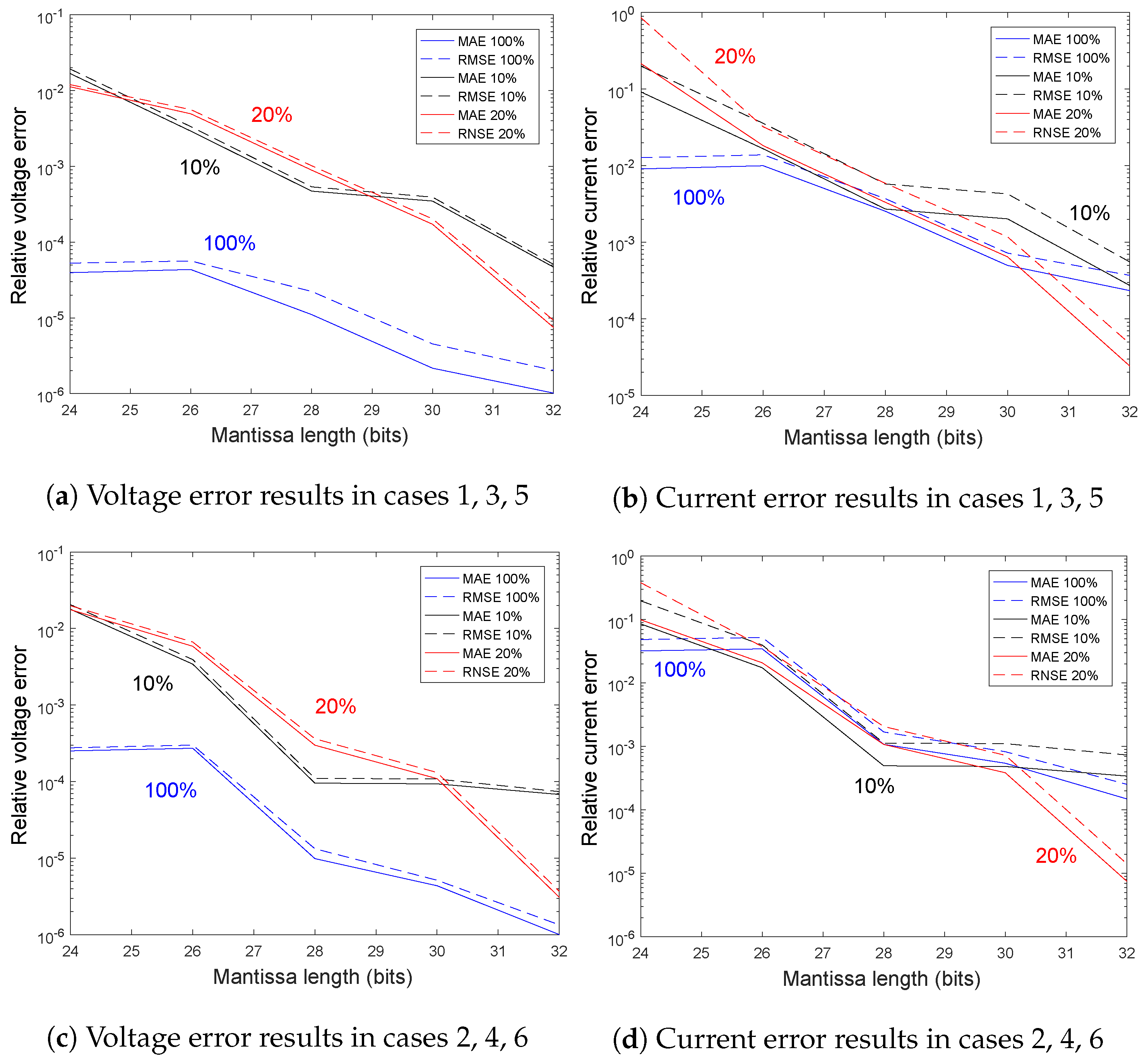
Figure 4 shows the MAE and RMSE for the inductor current and capacitor voltage in every scenario, relative to the RMS current and RMS voltage respectively. It can be seen that the voltage calculation is more sensitive to the variable width, which is consistent with Table 3, as the width for the current variable is less restrictive. As Table 3 predicted, the scenarios with 100% of load improve when the capacitor voltage is stored using 26 bits or more. Likewise, scenarios with 20% and 10% of load improve over 30 bits.
There are several cases that are worth mentioning. For instance, Figure 5 shows the capacitor voltage of case 6 (10% of load and voltage transient). It can be seen that, using 24 bits for the significand field, the capacitor voltage not only does not decrease but even increases. This is due to the insufficient resolution of the output voltage. As Table 3 shows that at least 30 bits are needed for the voltage state variable. The capacitor voltage increments are when it is increasing and when it is decreasing. Taking into account that the voltage is around 400 V and the output current is around 0.1 A, the negative increments are around V and V is rounded to 400 V when using 24 bits for the significand. When the switch is on, the current inductor reaches 1 A and, after switch-off, positive increments are around V, and V is rounded to V using 24 bits for the significand. Therefore, the problem is that is so small that it is rounded to 0 when it is compared with the actual capacitor voltage. However, is numerically bigger, so it is not rounded to 0, and the capacitor voltage only increases until the model reaches steady state.
Case 3 is another interesting simulation (20% of load without voltage transient), which can be seen in Figure 6. In this scenario, the system is in DCM as the load is low. When using 24 bits, the output voltage decreases due to resolution problems, until it crosses the limit between DCM and CCM. However, the duty cycles are calculated to operate in DCM and the simulation is in open loop, so they are not modified. As the DCM mode needs higher duty cycles than CCM for the same values of input and output voltages, when the model enters CCM mode, the inductor suffers a short but pronounced transient. The system does not become unstable because the current transient is followed by a growth of the capacitor voltage, and the model comes back to the DCM mode.
As stated, depending on the scenarios and the variable widths, some simulations offer completely wrong waveforms. The previous statistics—MAE and RMSE—give an idea of the simulation error but do not provide clear information about the similarity of the waveforms in terms of tendency. Therefore, another statistic could be found to achieve that. The PCC (Pearson Correlation Coefficient) measures the correlation between a model and its reference, so it also offers a quick test to know if the signs of a state variable and its reference match (positive when matching and negative otherwise). The Pearson correlations for all scenarios are presented in Table 4.
As almost all the simulations present relatively similar waveforms, the PCC is around 1 in almost all cases. In fact, the case of Figure 6 presents a PCC of 0.8311, because the waveforms tendency is similar most of the time, but the current transient worsens this similarity. The case of Figure 5 gives a negative PCC because the signs of the capacitor voltage tendency are opposite. It can be seen that, only when the PCC is over 0.999, the errors of Figure 4 may be acceptable. It is also important to note that the MAE and RMSE statistics make sense only when the tendencies of the tested simulation and its reference are similar. In other words, the similarity in the tendency is reached before the error reaches acceptable values. A comparison of Table 3 and Table 4 shows that the results are coherent. The theoretical widths are 26+n, 29+n and 30+n bits for 100%, 20% and 10% of load respectively, while the PCC results show that the simulations are sufficiently similar to their references (in terms of tendency) with 24, 28 and 32 bits.
As Table 3 shows, the necessary width for the current is much smaller than the voltage width. However, the current error of Figure 4 is similar to the voltage error using the same widths. The reason for such similarity is that both state variables depend on each other, and the accuracy issues of one variable affect the other one, so the worst case—the maximum width—should be considered.
Taking all the results into account, some conclusions can be reached regarding the necessary variable widths. First of all, the waveforms of the state variables should be similar to their references. This similarity can be measured using the PCC and selecting only the widths that obtain a PCC above 0.999, and taking the worst case – the most sensitive state variable. The previous step may choose insufficient widths. For instance, the case of 28 bits and 20% of load has a PCC of 1.0, but the MAE and RMSE errors are relatively high (around 0.5%), however, with 30 bits, the PCC is 0.993, while the MAE and RMSE errors drop to 0.1%. Therefore, once PCC has chosen a reasonable width, RMSE should also be considered. Errors below 0.1% may be sufficient for almost any application. It is possible to increase even more the width to reduce the numerical resolution error, but it is important to note that the model inherently has other error sources, such as non-idealities that have not been modeled, or tolerances in the values of C, R, etc.
For example, for this application we should look for widths that produce a PCC over 0.999 and MAE or RMSE between 0.1% and 0.5% in both state variables. These constraints would imply 28–30 bits for 100% load, 30–32 for 20% load and also 30–32 bits for 10% load. Table 3 predicts these results when using n = 2 or n = 4, verifying that the method proposed in Section 3 is a good approximation to determine the necessary width of state variables without having to run long simulations.
5. Synthesis Results
In this work, the synthesis is targeted to a device of the Arria 10 FPGA family using the Quartus Prime version 17.0 Standard Edition tool configured with the default parameters and automatic constraints except for the required clock period.
Table 5 shows area and time results for several significand widths, s. On the one hand, the area occupied in the target device for the converter is studied in terms of the logic utilization in ALMs (Adaptive Logic Module), total registers, number of DSP Blocks inferred by the synthesizer, and number of required pins. On the other hand, the maximum clock frequency for each converter configuration is evaluated. The constraint for the CLK period was set such that the synthesis and fitter (place and route) tools generate the fastest circuits.
Concerning time results, the circuit speed worsens at a rate of 1.5% per additional bit in the significand, while the area does so at the higher rate of 4%. It means that this architecture is more tolerant, in terms of speed, to resolution improvements than it is in terms of area, which is good for real-time simulations. Furthermore, the selected device, one of the largest in this family, has 427,200 ALMs.
Area and speed are closely related in digital circuits. In this case, although DSP blocks in the Arria 10 family have dedicated single-precision floating-point operators implemented in silicon, these resources are not inferred by the HDL synthesizer. Instead, the synthesizer configures the DSP block to compute the significand-part fixed-point operations. Therefore, similar results should be obtained using other FPGA families.
As the results have shown, the significand-part growth has not influenced the hardware usage or the maximum achievable frequency significantly. Therefore, the estimation method explained in Section 3, using a value between 4 and 6 for n, is valid. The simulations done in Section 4 are not necessary to estimate the state variable widths, but they were accomplished to demonstrate the validity of the method.
6. Conclusions
Thanks to the improvement in the performance of digital devices, HIL systems are starting to be used in applications that require small simulation steps (below s). The reduction of the simulation step allows more accurate simulations or make it possible to apply the technique to systems with higher natural frequencies, but the integration increments are inherently reduced. This can cause resolution problems if the arithmetics cannot handle values which are so small compared with the actual values of the state variables. In FPGA-based HIL applications, 32-bit floating-point is the most widely used arithmetic because of its simplicity from the designer point of view, along with its good performance compared with 64-bit floating-point. However, 32-bit floating-point numerical resolution is not suitable for all applications as it was observed in this work. Instead of using 64-bit arithmetics, intermediate widths can be chosen. This work has shown the limits of 32-bit floating-point for HIL simulations, and it has also provided a method to calculate the optimal width, taking into account the accuracy and the performance of the HIL system. Results have proven that the addition of few bits can dramatically improve the accuracy of the simulation but, once the numerical resolution is better than the increments, it is unproductive to increase the width.
Author Contributions
Conceptualization, A.S. and A.d.C.; methodology, A.S. and A.d.C.; software, E.T.; validation, E.T.; writing—original draft preparation and writing—review and editing, A.S., E.T. and A.d.C.
Funding
This research was funded by Spanish Ministerio de Economía y Competitividad grant number TEC2013-43017-R.
Conflicts of Interest
The authors declare no conflict of interest.
References
- Patella, B.J.; Prodic, A.; Zirger, A.; Maksimovic, D. High-frequency digital PWM controller IC for DC-DC converters. IEEE Trans. Power Electron. 2003, 18, 438–446. [Google Scholar] [CrossRef] [Green Version]
- Peterchev, A.V.; Xiao, J.; Sanders, S.R. Architecture and IC implementation of a digital VRM controller. IEEE Trans. Power Electron. 2003, 18, 356–364. [Google Scholar] [CrossRef] [Green Version]
- Albatran, S.; Smadi, I.A.; Ahmad, H.J.; Koran, A. Online Optimal Switching Frequency Selection for Grid-Connected Voltage Source Inverters. Electronics 2017, 6, 110. [Google Scholar] [CrossRef]
- Nguyen, T.D.; Hobraiche, J.; Patin, N.; Friedrich, G.; Vilain, J. A Direct Digital Technique Implementation of General Discontinuous Pulse Width Modulation Strategy. IEEE Trans. Ind. Electron. 2011, 58, 4445–4454. [Google Scholar] [CrossRef]
- Güvengir, U.; Çadırcı, I.; Ermiş, M. On-Line Application of SHEM by Particle Swarm Optimization to Grid-Connected, Three-Phase, Two-Level VSCs with Variable DC Link Voltage. Electronics 2018, 7, 151. [Google Scholar] [CrossRef]
- Champagne, R.; Dessaint, L.A.; Fortin-Blanchette, H. Real-time simulation of electric drives. Math. Comput. Simul. 2003, 63, 173–181. [Google Scholar] [CrossRef]
- Short, M.; Abugchem, F.; Abrar, U. Dependable Control for Wireless Distributed Control Systems. Electronics 2015, 4, 857–878. [Google Scholar] [CrossRef] [Green Version]
- Dennetière, S.; Saad, H.; Clerc, B.; Mahseredjian, J. Setup and performances of the real-time simulation platform connected to the INELFE control system. Electr. Power Syst. Res. 2016, 138, 180–187. [Google Scholar] [CrossRef]
- Barragan, L.A.; Urriza, I.; Navarro, D.; Artigas, J.I.; Acero, J.; Burdio, J.M. Comparing simulation alternatives of FPGA-based controllers for switching converters. In Proceedings of the 2007 IEEE International Symposium on Industrial Electronics, Vigo, Spain, 4–7 June 2007; pp. 419–424. [Google Scholar] [CrossRef]
- Short, M.; Abugchem, F. A Microcontroller-Based Adaptive Model Predictive Control Platform for Process Control Applications. Electronics 2017, 6, 88. [Google Scholar] [CrossRef]
- Viola, F.; Romano, P.; Miceli, R. Finite-Difference Time-Domain Simulation of Towers Cascade Under Lightning Surge Conditions. IEEE Trans. Ind. Appl. 2015, 51, 4917–4923. [Google Scholar] [CrossRef]
- Aiello, G.; Cacciato, M.; Scarcella, G.; Scelba, G. Failure analysis of AC motor drives via FPGA-based hardware-in-the-loop simulations. Electr. Eng. 2017, 99, 1337–1347. [Google Scholar] [CrossRef]
- Herrera, L.; Li, C.; Yao, X.; Wang, J. FPGA-Based Detailed Real-Time Simulation of Power Converters and Electric Machines for EV HIL Applications. IEEE Trans. Ind. Appl. 2015, 51, 1702–1712. [Google Scholar] [CrossRef]
- Sandre-Hernandez, O.; Rangel-Magdaleno, J.; Morales-Caporal, R.; Bonilla-Huerta, E. HIL simulation of the DTC for a three-level inverter fed a PMSM with neutral-point balancing control based on FPGA. Electr. Eng. 2018, 100, 1441–1454. [Google Scholar] [CrossRef]
- Morales-Caporal, M.; Rangel-Magdaleno, J.; Peregrina-Barreto, H.; Morales-Caporal, R. FPGA-in-the-loop simulation of a grid-connected photovoltaic system by using a predictive control. Electr. Eng. 2018, 100, 1327–1337. [Google Scholar] [CrossRef]
- Waidyasooriya, H.M.; Takei, Y.; Tatsumi, S.; Hariyama, M. OpenCL-Based FPGA-Platform for Stencil Computation and Its Optimization Methodology. IEEE Trans. Parallel Distrib. Syst. 2017, 28, 1390–1402. [Google Scholar] [CrossRef]
- Fernández-Álvarez, A.; Portela-García, M.; García-Valderas, M.; López, J.; Sanz, M. HW/SW Co-Simulation System for Enhancing Hardware-in-the-Loop of Power Converter Digital Controllers. IEEE J. Emerg. Sel. Top. Power Electron. 2017, 5, 1779–1786. [Google Scholar] [CrossRef]
- Typhoon HIL. Available online: https://www.typhoon-hil.com (accessed on 11 December 2017).
- dSPACE. Available online: https://www.dspace.com (accessed on 11 December 2017).
- OPAL-RT. Available online: https://www.opal-rt.com (accessed on 11 December 2017).
- Sanchez, A.; de Castro, A.; Garrido, J. A Comparison of Simulation and Hardware-in-the-Loop Alternatives for Digital Control of Power Converters. IEEE Trans. Ind. Inform. 2012, 8, 491–500. [Google Scholar] [CrossRef]
- Razzaghi, R.; Mitjans, M.; Rachidi, F.; Paolone, M. An automated FPGA real-time simulator for power electronics and power systems electromagnetic transient applications. Electr. Power Syst. Res. 2016, 141, 147–156. [Google Scholar] [CrossRef]
- MacCleery, B.; Trescases, O.; Mujagic, M.; Bohls, D.M.; Stepanov, O.; Fick, G. A new platform and methodology for system-level design of next-generation FPGA-based digital SMPS. In Proceedings of the 2012 IEEE Energy Conversion Congress and Exposition (ECCE), Raleigh, NC, USA, 15–20 September 2012; pp. 1599–1606. [Google Scholar] [CrossRef]
- Parma, G.; Dinavahi, V. Real-Time Digital Hardware Simulation of Power Electronics and Drives. IEEE Trans. Power Deliv. 2007, 22, 1235–1246. [Google Scholar] [CrossRef]
- Matar, M.; Iravani, R. Massively Parallel Implementation of AC Machine Models for FPGA-Based Real-Time Simulation of Electromagnetic Transients. IEEE Trans. Power Deliv. 2011, 26, 830–840. [Google Scholar] [CrossRef]
- Myaing, A.; Dinavahi, V. FPGA-Based Real-Time Emulation of Power Electronic Systems with Detailed Representation of Device Characteristics. IEEE Trans. Ind. Electron. 2011, 58, 358–368. [Google Scholar] [CrossRef]
- Lucia, O.; Urriza, I.; Barragan, L.A.; Navarro, D.; Jimenez, O.; Burdio, J.M. Real-Time FPGA-Based Hardware-in-the-Loop Simulation Test Bench Applied to Multiple-Output Power Converters. IEEE Trans. Ind. Appl. 2011, 47, 853–860. [Google Scholar] [CrossRef]
- Sanchez, A.; Todorovich, E.; de Castro, A. Impact of the hardened floating-point cores on HIL technology. Electr. Power Syst. Res. 2018, 165, 53–59. [Google Scholar] [CrossRef]
- Infineon Technologies AG. Design Note: CCM PFC Boost Converter Design (DN 2013-01); Rev. 1.0.; Infineon Technologies AG: Neubiberg, Germany, 2013. [Google Scholar]
- Butcher, J.C. The Numerical Analysis of Ordinary Differential Equations: Runge-Kutta and General Linear Methods; Wiley-Interscience: New York, NY, USA, 1987. [Google Scholar]
- Ibarra, L.; Rosales, A.; Ponce, P.; Molina, A.; Ayyanar, R. Overview of Real-Time Simulation as a Supporting Effort to Smart-Grid Attainment. Energies 2017, 10, 817. [Google Scholar] [CrossRef]
- Saralegui, R.; Sanchez, A.; Martínez-García, M.S.; Novo, J.; de Castro, A. Comparison of Numerical Methods for Hardware-In-the-Loop Simulation of Switched-Mode Power Supplies. In Proceedings of the 2018 IEEE 19th Workshop on Control and Modeling for Power Electronics (COMPEL), Padova, Italy, 25–28 June 2018; pp. 1–6. [Google Scholar] [CrossRef]
- Sutikno, T.; Idris, N.R.N.; Jidin, A.Z.; Daud, M.Z. FPGA based high precision torque and flux estimator of direct torque control drives. In Proceedings of the 2011 IEEE Applied Power Electronics Colloquium (IAPEC), Johor Bahru, Malaysia, 18–19 April 2011; pp. 122–127. [Google Scholar] [CrossRef]
- Goñi, O.; Sanchez, A.; Todorovich, E.; de Castro, A. Resolution Analysis of Switching Converter Models for Hardware-in-the-Loop. IEEE Trans. Ind. Inf. 2014, 10, 1162–1170. [Google Scholar] [CrossRef] [Green Version]
- IEEE Standard for Floating-Point Arithmetic; IEEE Std 754-2008; IEEE Standards: Piscataway, NJ, USA, 2008; pp. 1–70. [CrossRef]
- IEEE Standard VHDL Language Reference Manual; IEEE Std 1076-2008 (Revision of IEEE Std 1076-2002); IEEE Standards: Piscataway, NJ, USA, 2009; pp. 1–626. [CrossRef]
- Merfert, I. Analysis and application of a new control method for continuous-mode boost converters in power factor correction circuits. In Proceedings of the PESC97, Record 28th Annual IEEE Power Electronics Specialists Conference, Formerly Power Conditioning Specialists Conference 1970-71, Power Processing and Electronic Specialists Conference 1972, Saint Louis, MO, USA, 27 June 1997; Volume 1, pp. 96–102. [Google Scholar] [CrossRef]
- Merfert, I.W. Stored-duty-ratio control for power factor correction. In Proceedings of the Fourteenth Annual Applied Power Electronics Conference and Exposition, APEC ’99, Dallas, TX, USA, 14–18 March 1999; Volume 2, pp. 1123–1129. [Google Scholar] [CrossRef]
- Sanchez, A.; de Castro, A.; López, V.M.; Azcondo, F.J.; Garrido, J. Single ADC Digital PFC Controller Using Precalculated Duty Cycles. IEEE Trans. Power Electron. 2014, 29, 996–1005. [Google Scholar] [CrossRef] [Green Version]
Figure 1.
Boost converter topology.

Figure 2.
Current and voltages waveforms of the PFC boost converter.

Figure 3.
IEEE-754 floating-point formats.

Figure 4.
MAE and RMSE results of every scenario.

Figure 5.
Simulation of 10% of load and a voltage transient (Case 6).

Figure 6.
Simulation of 20% of load (Case 3). (a) 100 ms of simulation. (b) Zoom between 40 and 50 ms.
Figure 6.
Simulation of 20% of load (Case 3). (a) 100 ms of simulation. (b) Zoom between 40 and 50 ms.


Table 1.
Boost converter parameters used in Section 4.
Table 1.
Boost converter parameters used in Section 4.
| Parameter | C | L | |||
|---|---|---|---|---|---|
| Value | 540.5 F | 416.5 H | 230 V | 400 V | 400 W |
Table 2.
Experimental scenarios for the boost model.
| Case 1 | Case 2 | Case 3 | Case 4 | Case 5 | Case 6 | |
|---|---|---|---|---|---|---|
| Output load | 100% | 100% | 20% | 20% | 10% | 10% |
| Starting capacitor voltage | 400 V | 410 V | 400 V | 410 V | 400 V | 410 V |
Table 3.
Significand length needed for optimal simulations using Equation (7).
Table 3.
Significand length needed for optimal simulations using Equation (7).
| 100% Load Case 1 & 2 | 20% Load Case 3 & 4 | 10% Load Case 5 & 6 | |
|---|---|---|---|
| 7 + n | 5 + n | 4 + n | |
| 26 + n | 29 + n | 30 + n |
Table 4.
Pearson correlation taking the capacitor voltage.
| Case 1 100% Steady | Case 2 100% Trans | Case 3 20% Steady | Case 4 20% Trans | Case 5 10% Steady | Case 6 10% Trans | |
|---|---|---|---|---|---|---|
| 24 bits | 1.0000 | 0.9991 | 0.8311 | 0.9832 | 0.8708 | 0.9712 |
| 26 bits | 0.9999 | 0.9990 | −0.0555 | 0.7582 | 0.9496 | −0.0685 |
| 28 bits | 1.0000 | 1.0000 | 1.0000 | 1.0000 | 0.9928 | 0.9980 |
| 30 bits | 1.0000 | 1.0000 | 0.9993 | 0.9998 | 0.9976 | 0.9980 |
| 32 bits | 1.0000 | 1.0000 | 1.0000 | 1.0000 | 1.0000 | 0.9994 |
Table 5.
Post place & route area and time results.
| Significand Width | 24 | 26 | 28 | 30 | 32 |
|---|---|---|---|---|---|
| ALMs | 4998 | 5413 | 5522 | 6146 | 6606 |
| Regs | 64 | 68 | 72 | 76 | 80 |
| DSP | 3 | 3 | 9 | 9 | 9 |
| Pins | 131 | 139 | 147 | 155 | 163 |
| CLK const. [ns] | 52 | 52 | 53 | 55 | 57 |
| Fmax [MHz] | 19.38 | 19.21 | 18.6 | 17.86 | 17.23 |
© 2018 by the authors. Licensee MDPI, Basel, Switzerland. This article is an open access article distributed under the terms and conditions of the Creative Commons Attribution (CC BY) license (http://creativecommons.org/licenses/by/4.0/).
Share and Cite
MDPI and ACS Style
Sanchez, A.; Todorovich, E.; De Castro, A. Exploring the Limits of Floating-Point Resolution for Hardware-In-the-Loop Implemented with FPGAs. Electronics 2018, 7, 219. https://doi.org/10.3390/electronics7100219
AMA Style
Sanchez A, Todorovich E, De Castro A. Exploring the Limits of Floating-Point Resolution for Hardware-In-the-Loop Implemented with FPGAs. Electronics. 2018; 7(10):219. https://doi.org/10.3390/electronics7100219
Chicago/Turabian StyleSanchez, Alberto, Elías Todorovich, and Angel De Castro. 2018. "Exploring the Limits of Floating-Point Resolution for Hardware-In-the-Loop Implemented with FPGAs" Electronics 7, no. 10: 219. https://doi.org/10.3390/electronics7100219
Note that from the first issue of 2016, this journal uses article numbers instead of page numbers. See further details here.