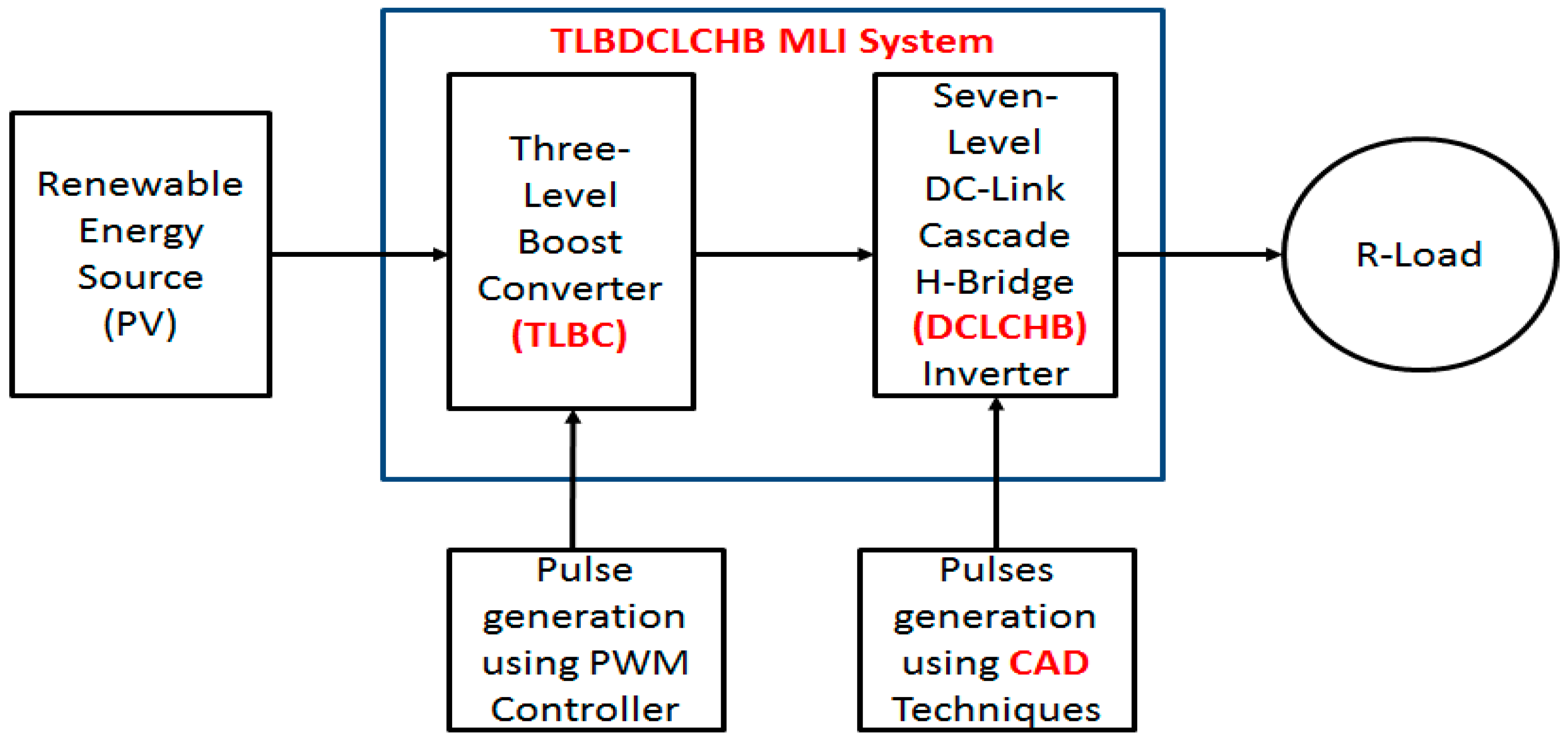
Figure 1.
Block diagram of the proposed (TLBDCLCHB MLI) system.
Figure 1.
Block diagram of the proposed (TLBDCLCHB MLI) system.
Figure 2.
Equivalent structure of TLBDCLCHB MLI system.
Figure 2.
Equivalent structure of TLBDCLCHB MLI system.
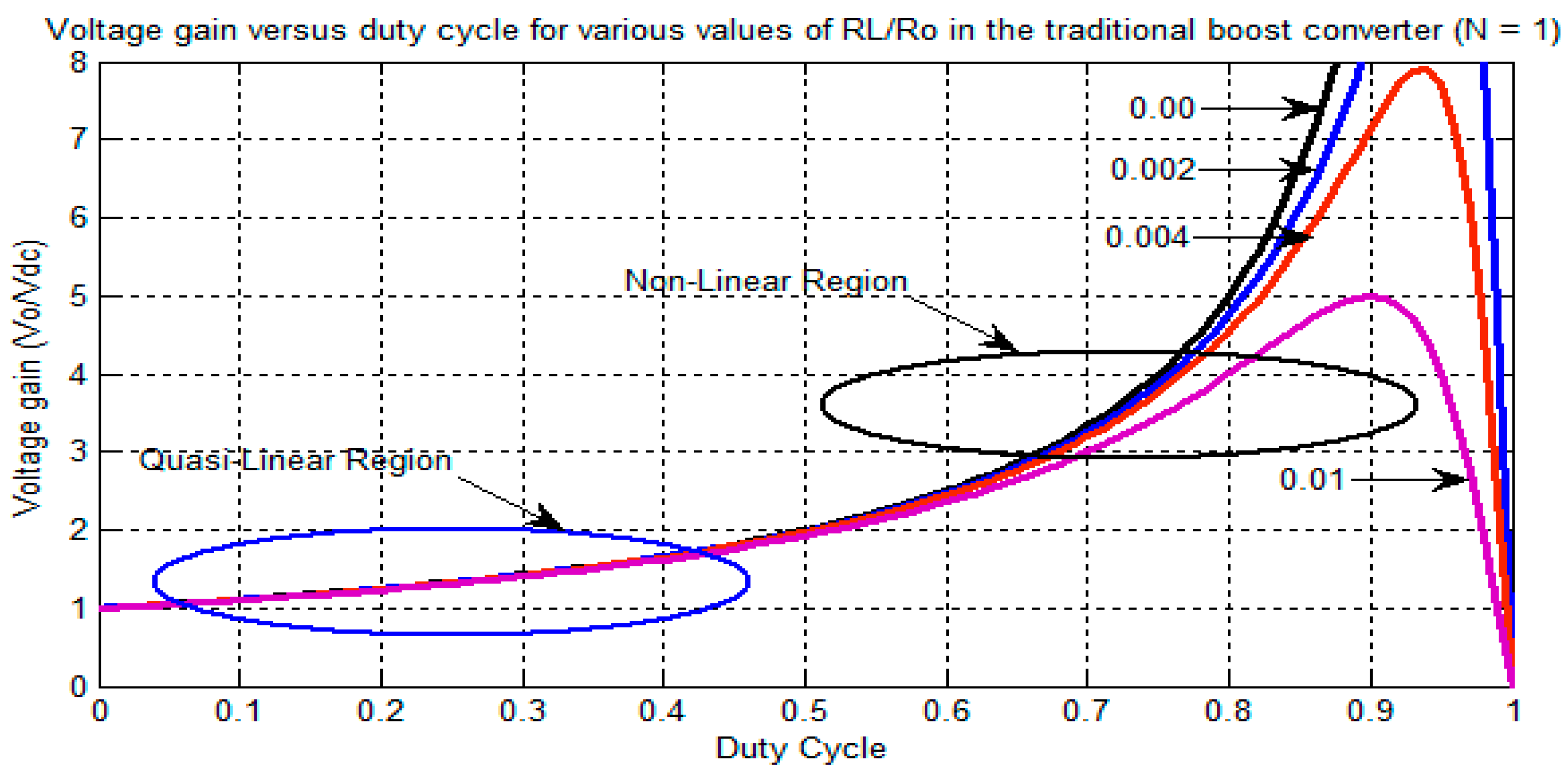
Figure 3.
Duty cycle versus voltage gain of a traditional boost converter for various values of RL/Ro (N = 1).
Figure 3.
Duty cycle versus voltage gain of a traditional boost converter for various values of RL/Ro (N = 1).
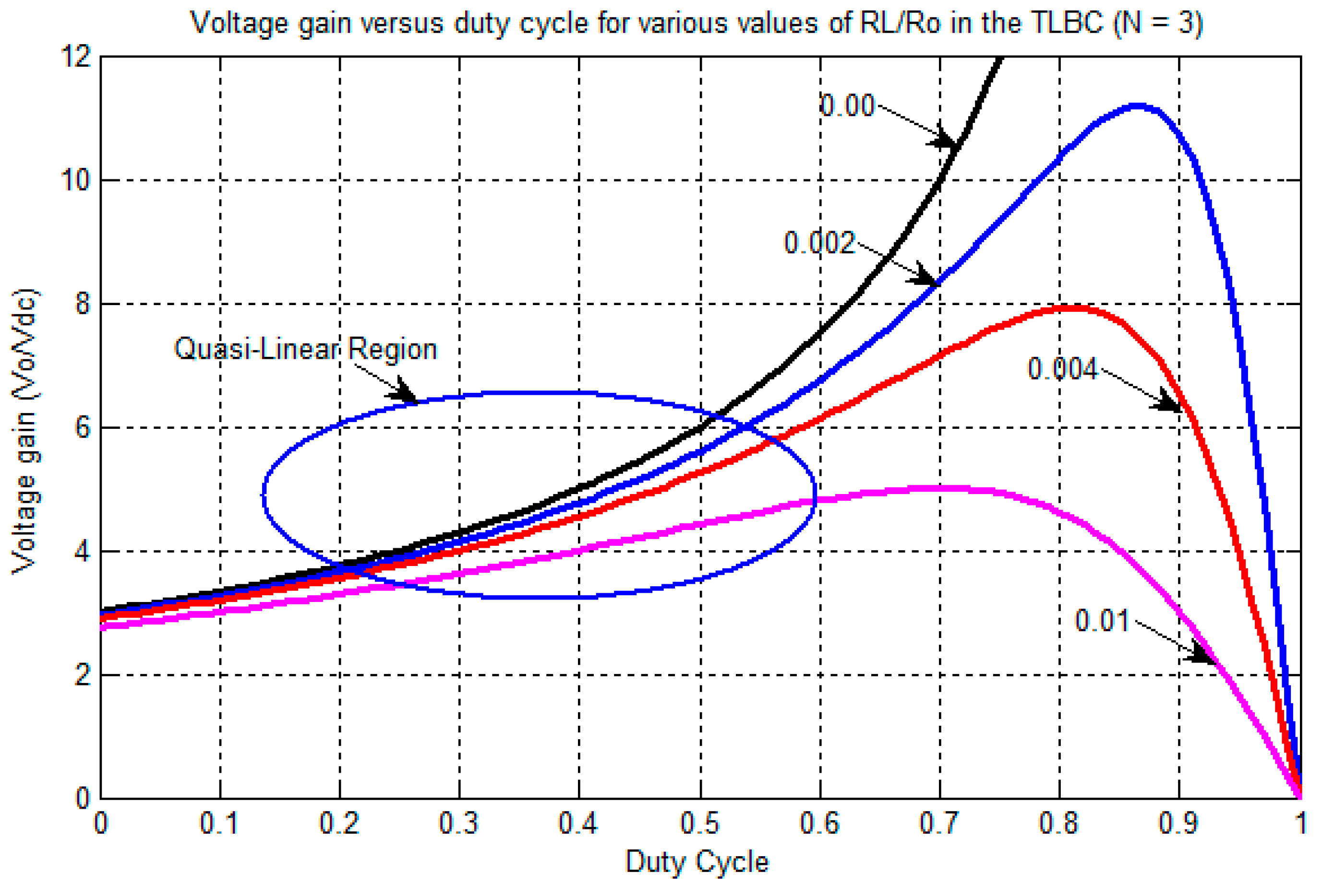
Figure 4.
Duty cycle versus voltage gain of TLBC for various values of RL/Ro (N = 3).
Figure 4.
Duty cycle versus voltage gain of TLBC for various values of RL/Ro (N = 3).
Figure 5.
Charging C5 of a TLBC with switch and diode’s voltage drop.
Figure 5.
Charging C5 of a TLBC with switch and diode’s voltage drop.
Figure 6.
Model of TLBC in closed-loop mode.
Figure 6.
Model of TLBC in closed-loop mode.
Figure 7.
Single-phase seven-level DCLCHB inverter.
Figure 7.
Single-phase seven-level DCLCHB inverter.
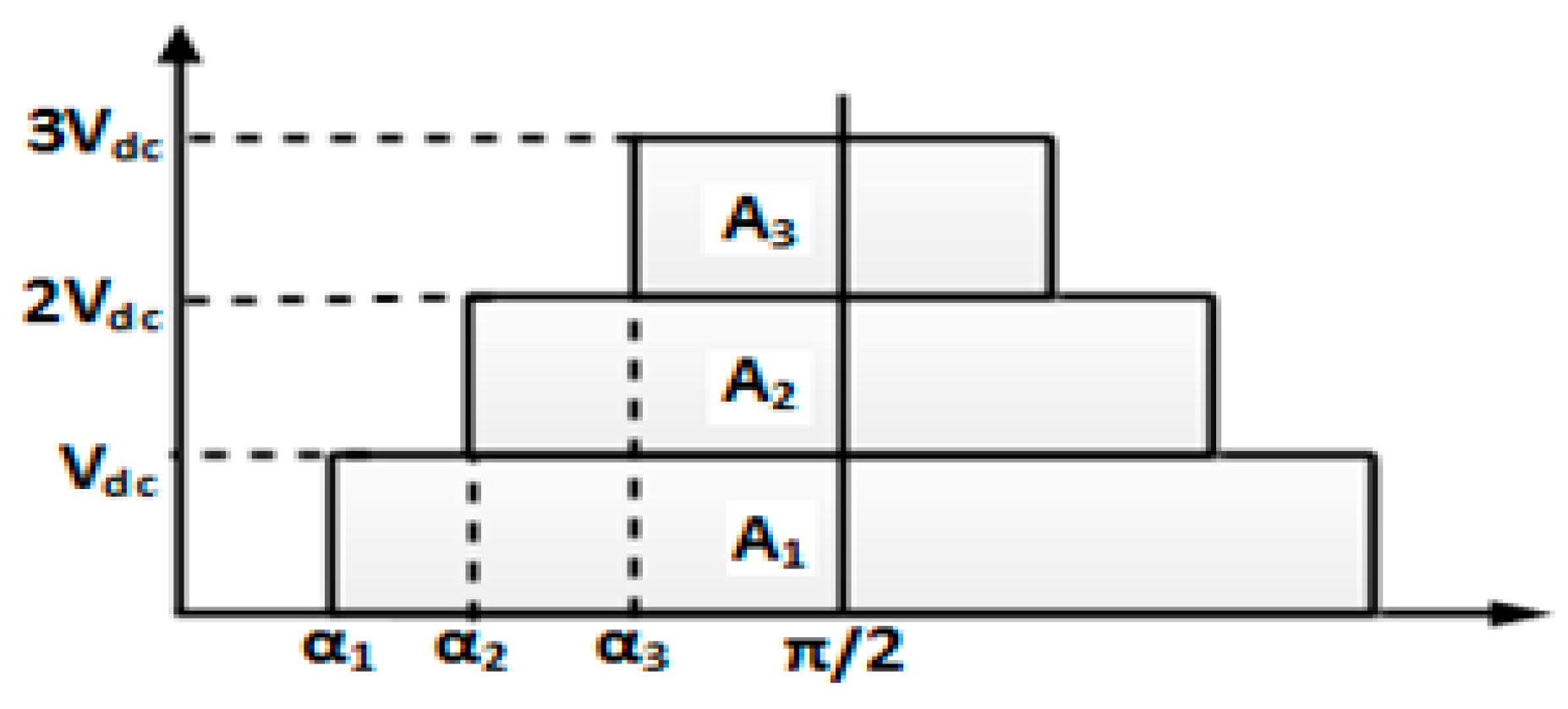
Figure 8.
Generation of the seven-level stepped voltage waveform for DCLCHB inverter using CAD techniques.
Figure 8.
Generation of the seven-level stepped voltage waveform for DCLCHB inverter using CAD techniques.
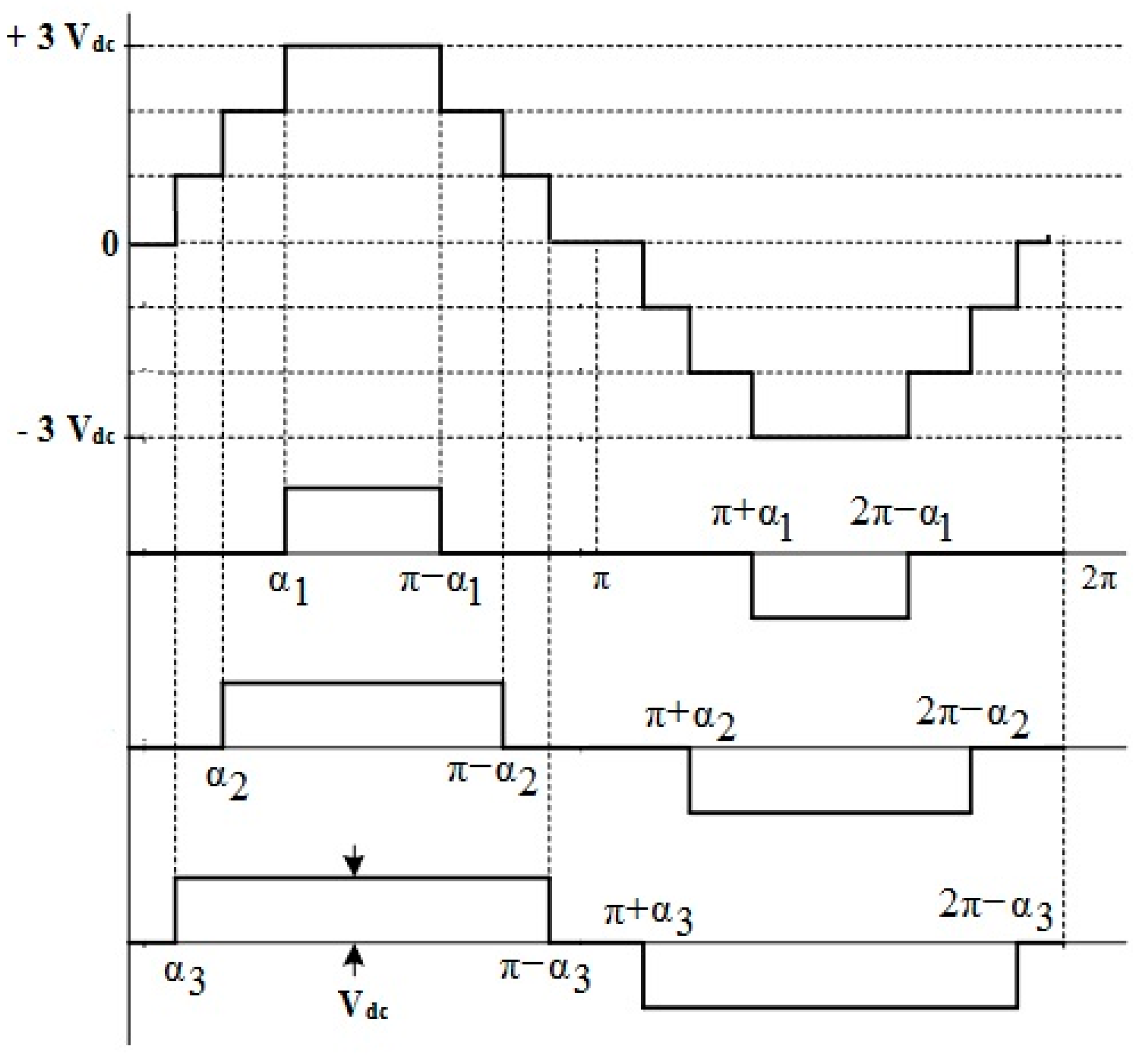
Figure 9.
Reference voltage waveform with dummy conducting angles.
Figure 9.
Reference voltage waveform with dummy conducting angles.
Figure 10.
Output phase-voltage of a seven-level DCLCHB inverter in the positive half-cycle voltage.
Figure 10.
Output phase-voltage of a seven-level DCLCHB inverter in the positive half-cycle voltage.
Figure 11.
Output of TLBC in open-loop for D = 0.4.
Figure 11.
Output of TLBC in open-loop for D = 0.4.
Figure 12.
Output of TLBC in open-loop for D = 0.5.
Figure 12.
Output of TLBC in open-loop for D = 0.5.
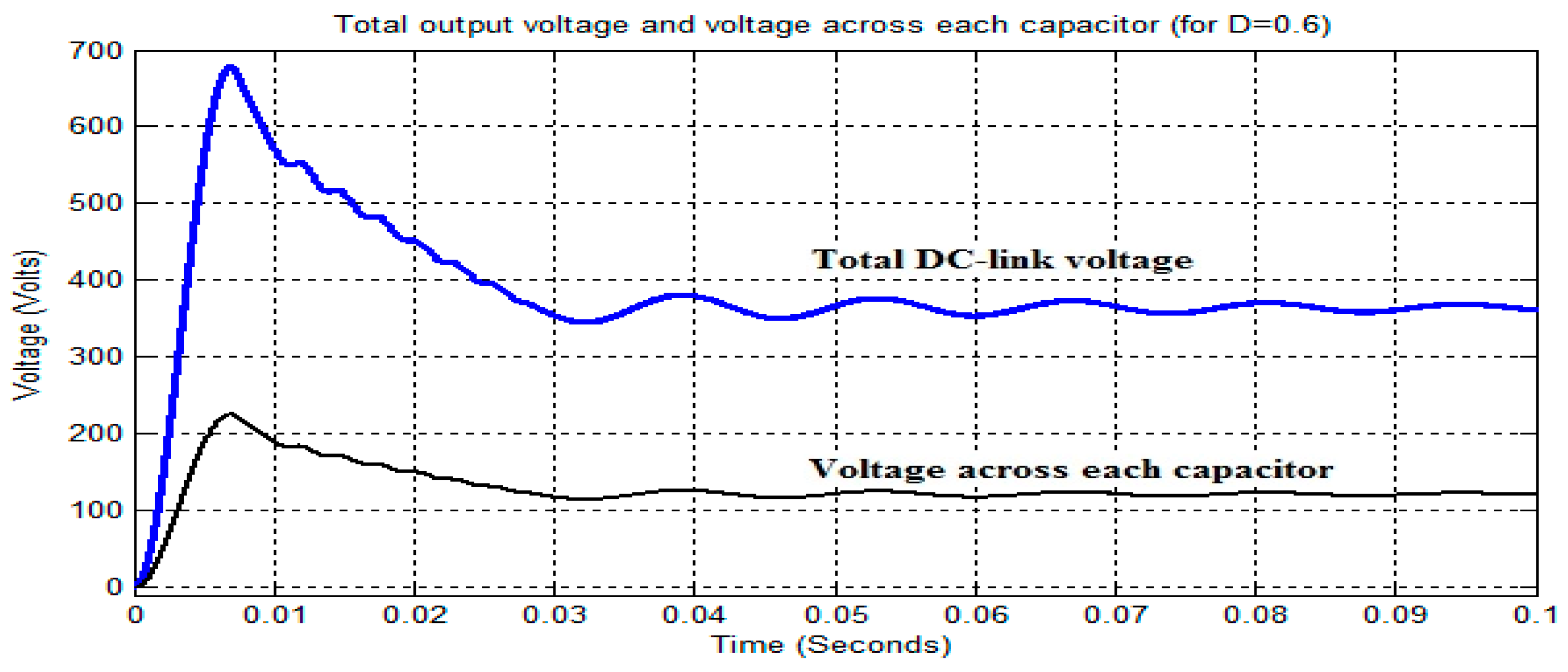
Figure 13.
Output of TLBC in open-loop for D = 0.6.
Figure 13.
Output of TLBC in open-loop for D = 0.6.
Figure 14.
Output of TLBC in closed-loop for D = 0.5.
Figure 14.
Output of TLBC in closed-loop for D = 0.5.
Figure 15.
Change in duty cycle of TLBC in closed-loop.
Figure 15.
Change in duty cycle of TLBC in closed-loop.
Figure 16.
Inverter output across LGU using the EPCAD technique.
Figure 16.
Inverter output across LGU using the EPCAD technique.
Figure 17.
TLBDCLCHB inverter output using EPCAD technique.
Figure 17.
TLBDCLCHB inverter output using EPCAD technique.
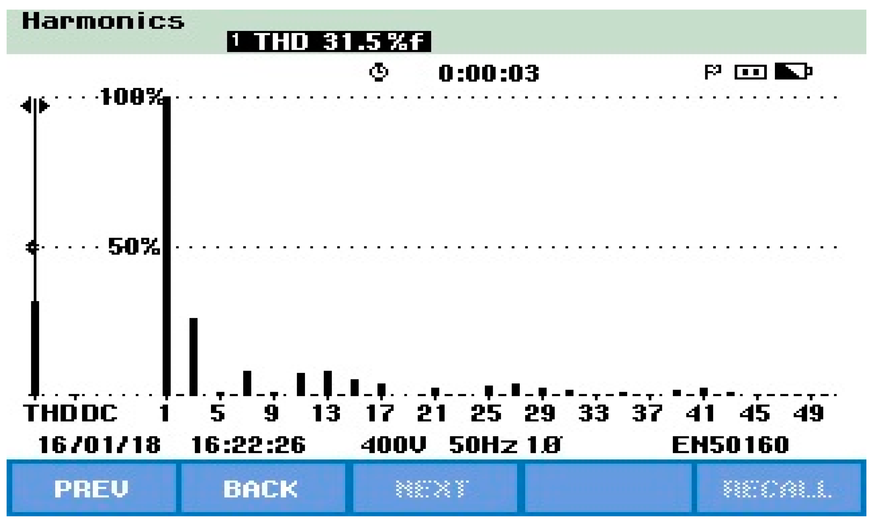
Figure 18.
THD analysis of TLBDCLCHB inverter output using EPCAD technique.
Figure 18.
THD analysis of TLBDCLCHB inverter output using EPCAD technique.
Figure 19.
Inverter output across LGU using the SPWCAD technique.
Figure 19.
Inverter output across LGU using the SPWCAD technique.
Figure 20.
TLBDCLCHB inverter output using the SPWCAD technique.
Figure 20.
TLBDCLCHB inverter output using the SPWCAD technique.
Figure 21.
THD analysis of the TLBDCLCHB inverter output using the SWPCAD technique.
Figure 21.
THD analysis of the TLBDCLCHB inverter output using the SWPCAD technique.
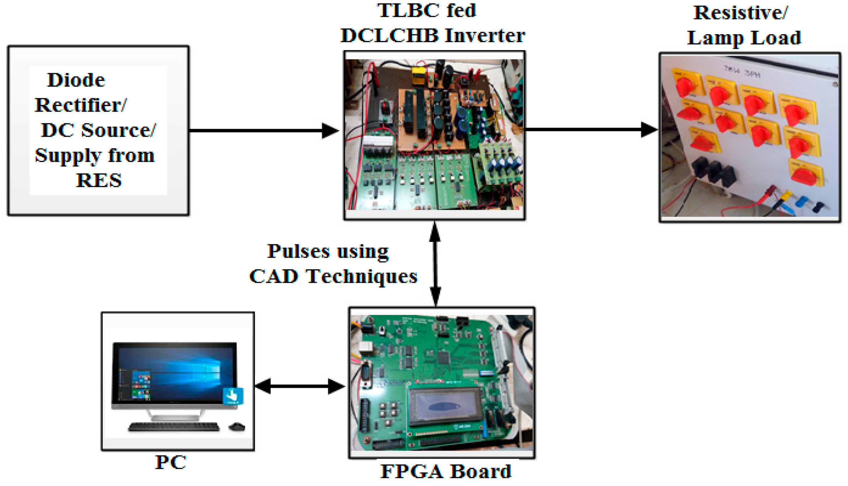
Figure 22.
Block diagram of the TLBDCLCHB hardware implementation.
Figure 22.
Block diagram of the TLBDCLCHB hardware implementation.
Figure 23.
Hardware implementation of the TLBDCLCHB inverter system with an FPGA controller.
Figure 23.
Hardware implementation of the TLBDCLCHB inverter system with an FPGA controller.
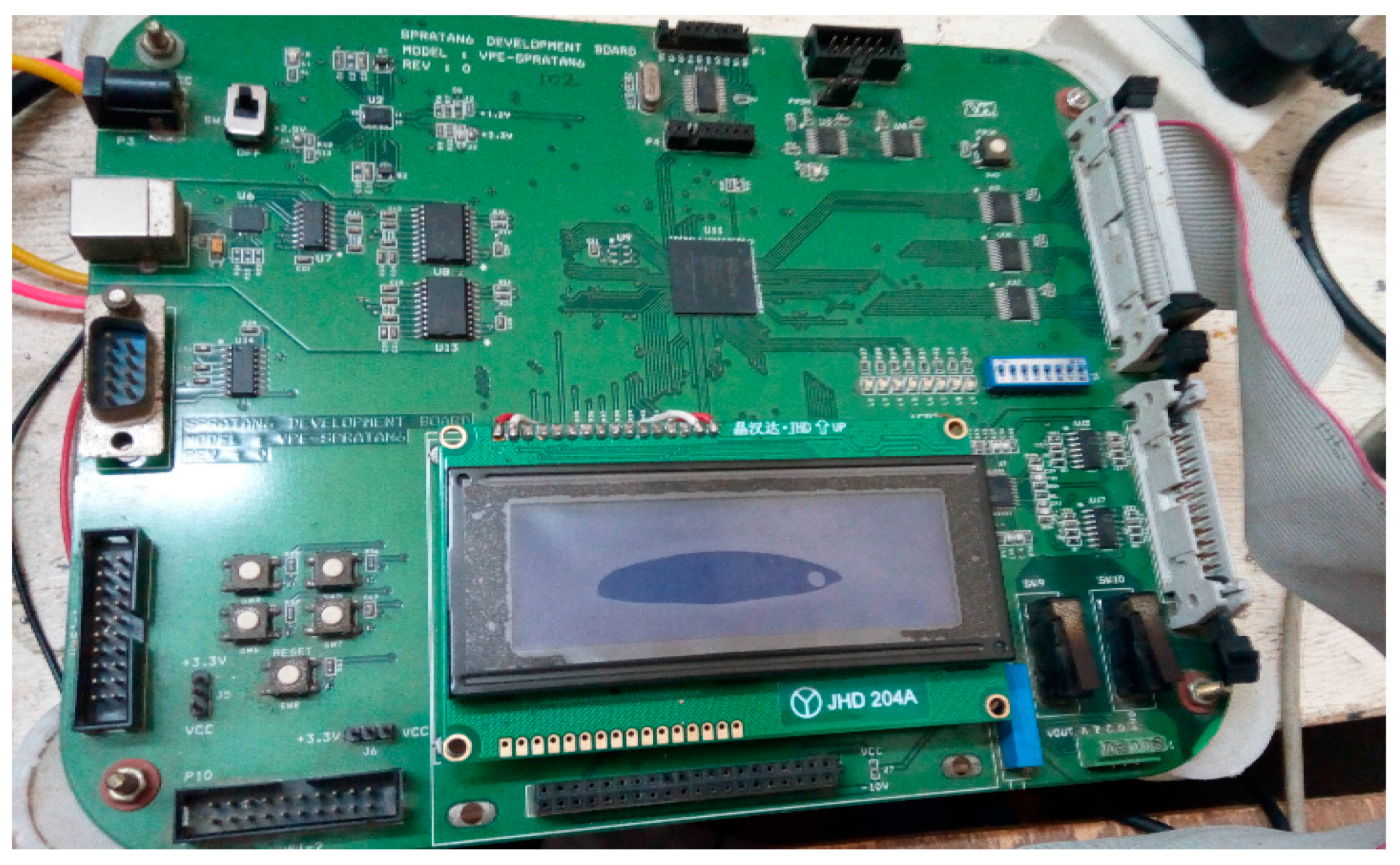
Figure 24.
Xilinx Spartan6 development board.
Figure 24.
Xilinx Spartan6 development board.
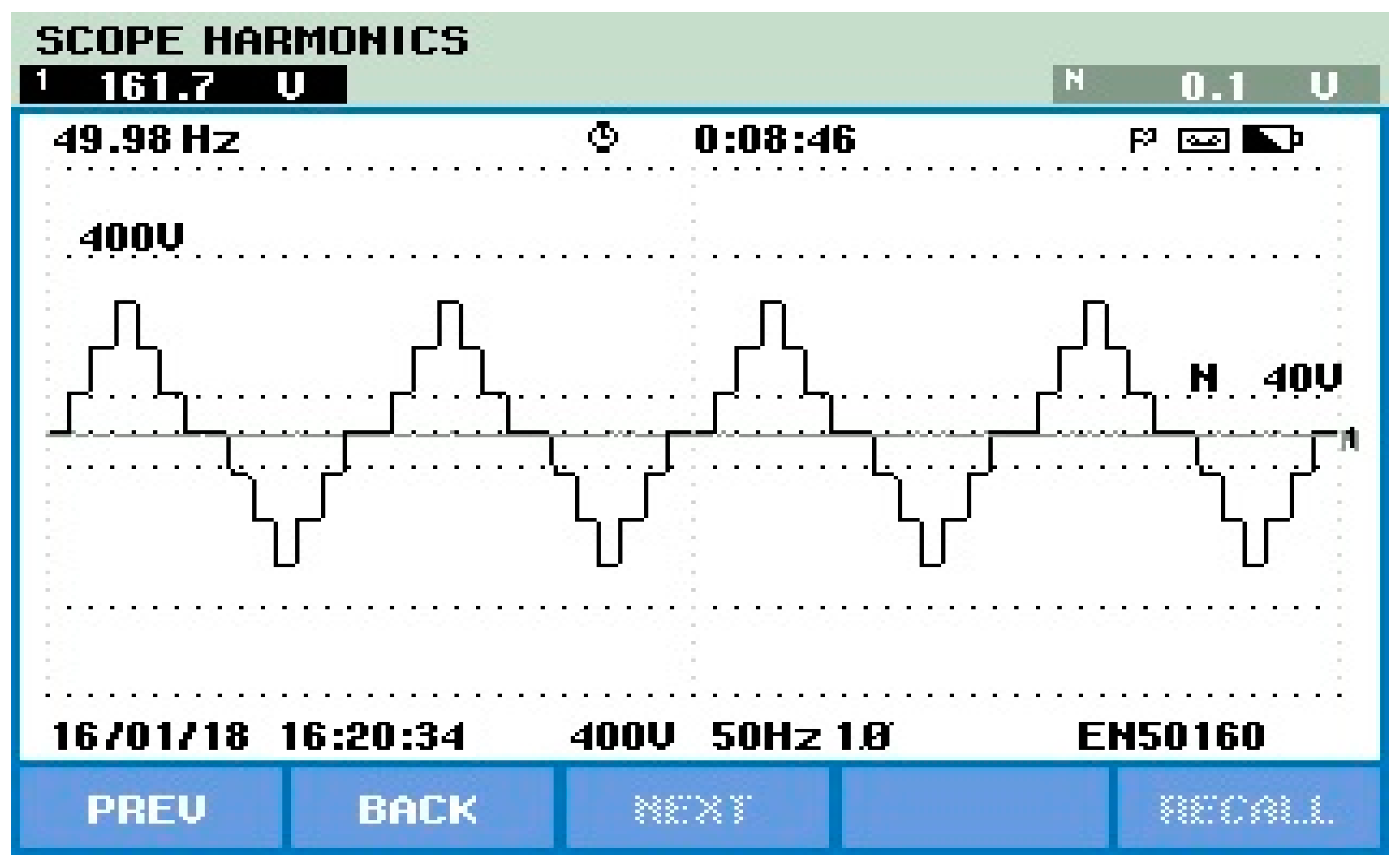
Figure 25.
Seven-level stepped output voltage of TLBC-fed DCLCHB inverter system.
Figure 25.
Seven-level stepped output voltage of TLBC-fed DCLCHB inverter system.
Figure 26.
Voltage across the capacitor CH1 and total DC-link voltage of TLBC CH2 for D = 0.5.
Figure 26.
Voltage across the capacitor CH1 and total DC-link voltage of TLBC CH2 for D = 0.5.
Figure 27.
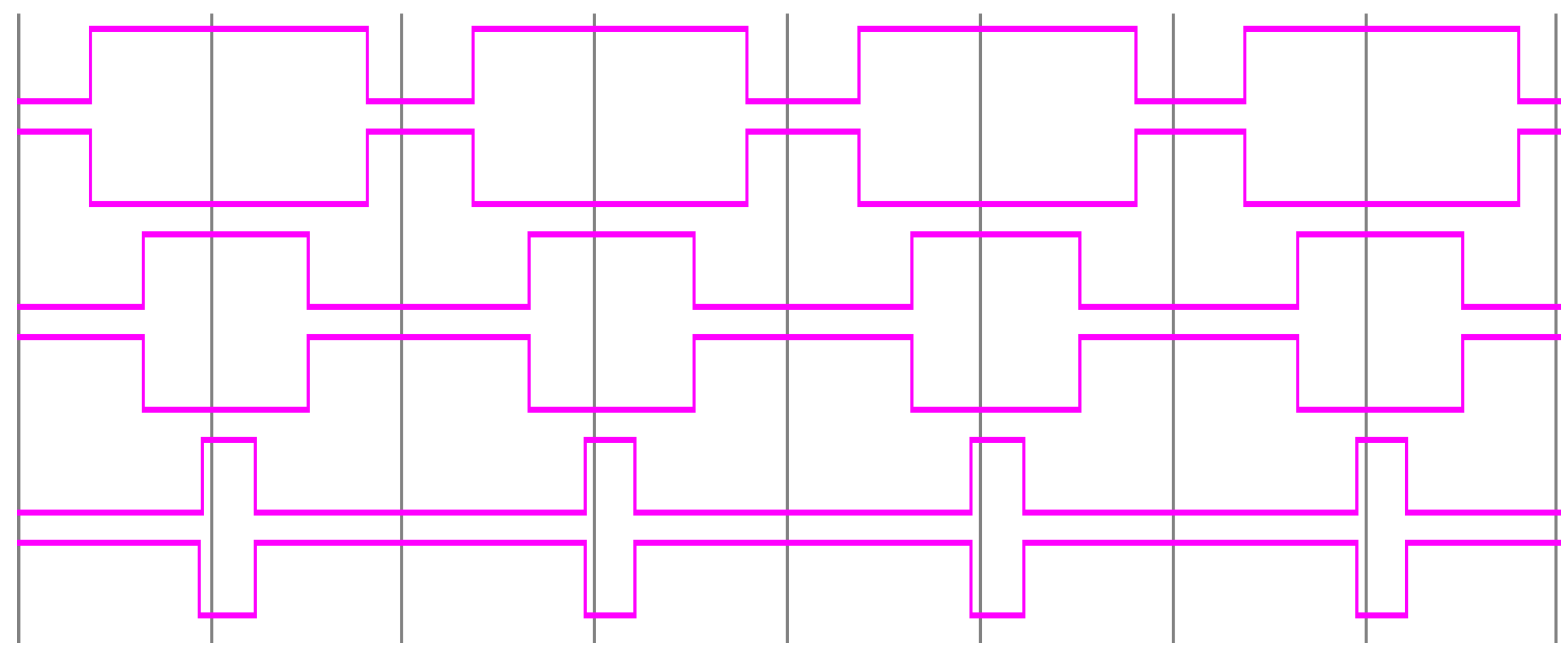
Generation of pulses for the LGU switches (S1 to S6) in the DCLCHB inverter using the EPCAD technique through Xilinx ISE.
Figure 27.
Generation of pulses for the LGU switches (S1 to S6) in the DCLCHB inverter using the EPCAD technique through Xilinx ISE.
Figure 28.
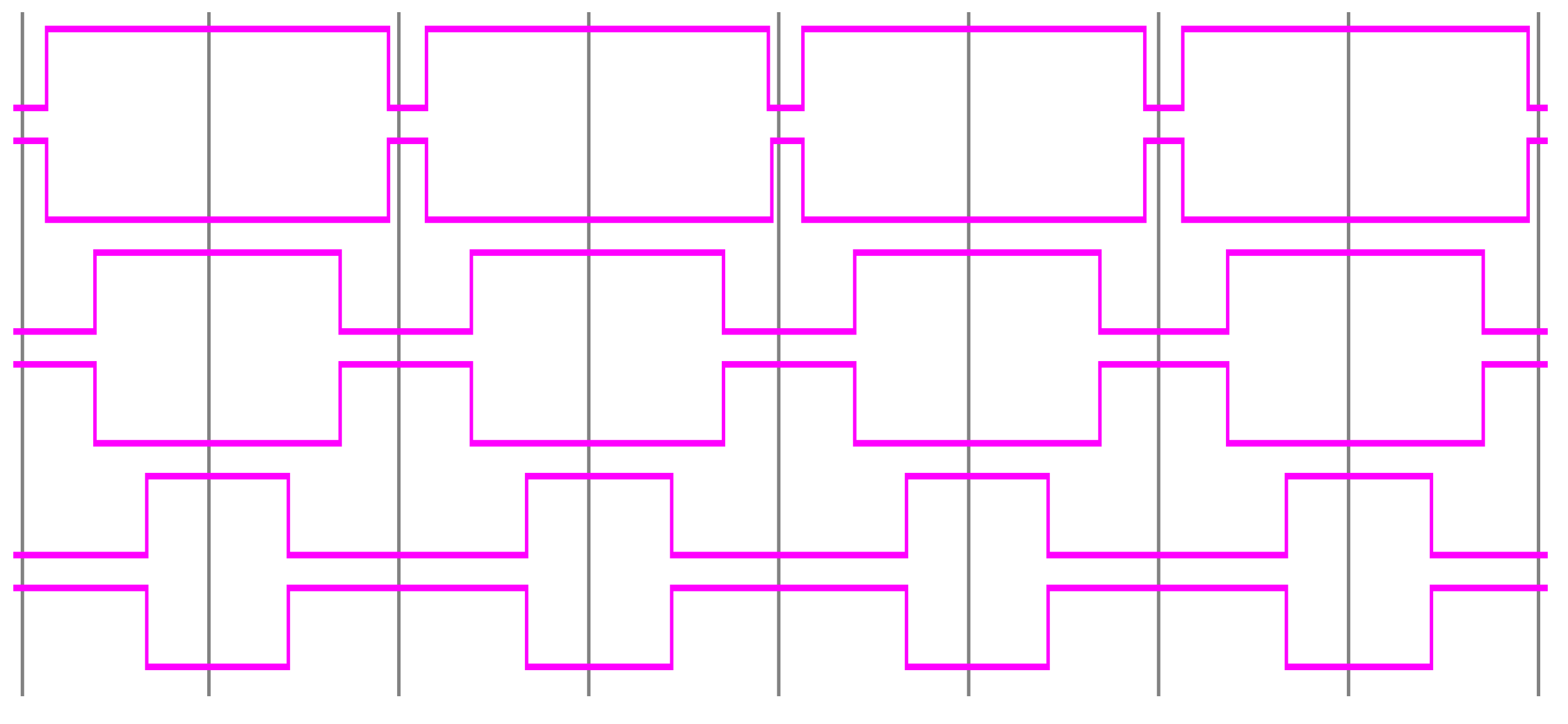
Generation of pulses for the LGU switches (S1 to S6) in the DCLCHB inverter using the SPWCAD technique through Xilinx ISE.
Figure 28.
Generation of pulses for the LGU switches (S1 to S6) in the DCLCHB inverter using the SPWCAD technique through Xilinx ISE.
Figure 29.
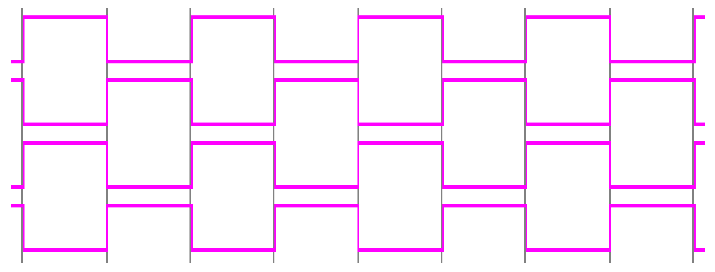
Generation of pulses for the PSGU switches (P1 to P4) in the DCLCHB inverter using a pulse generator through Xilinx ISE.
Figure 29.
Generation of pulses for the PSGU switches (P1 to P4) in the DCLCHB inverter using a pulse generator through Xilinx ISE.
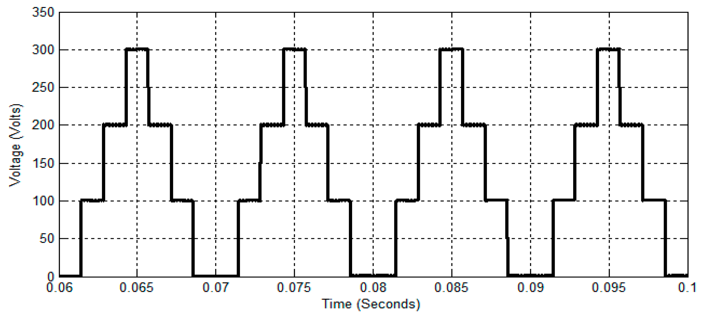
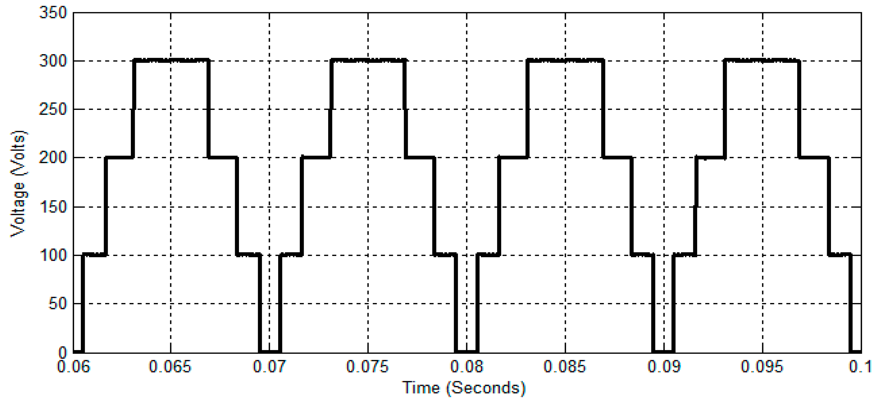
Figure 30.
TLBDCLCHB inverter output using the EPCAD technique.
Figure 30.
TLBDCLCHB inverter output using the EPCAD technique.
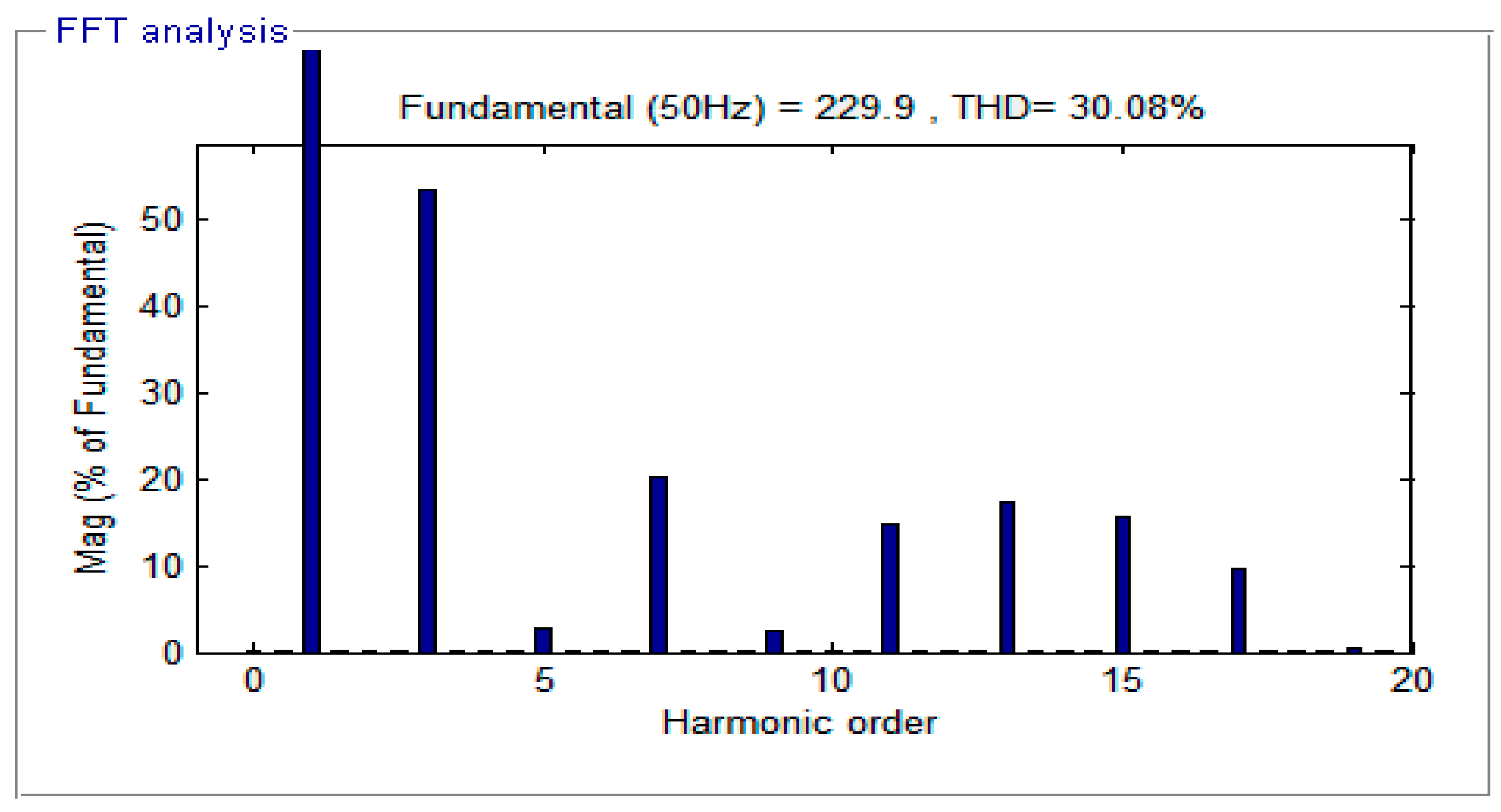
Figure 31.
THD analysis of the TLBDCLCHB inverter output using the EPCAD technique.
Figure 31.
THD analysis of the TLBDCLCHB inverter output using the EPCAD technique.
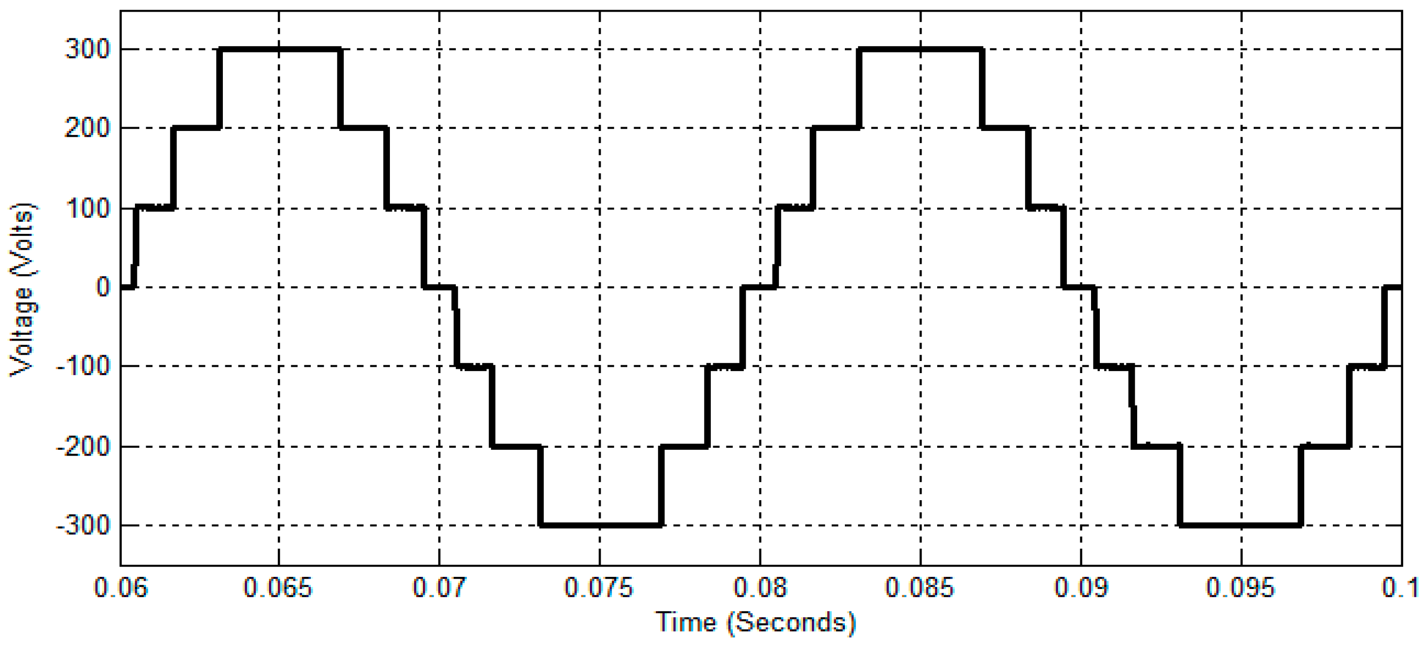
Figure 32.
TLBDCLCHB inverter output using the SPWCAD technique.
Figure 32.
TLBDCLCHB inverter output using the SPWCAD technique.
Figure 33.
THD analysis of the TLBDCLCHB inverter output using the SPWCAD technique.
Figure 33.
THD analysis of the TLBDCLCHB inverter output using the SPWCAD technique.
Table 1.
Component requirements for existing and proposed boost based MLI systems.
Table 1.
Component requirements for existing and proposed boost based MLI systems.
| Number of Levels | Boost Cascade MLI (Conventional) | TLBDCLCHB MLI (Proposed) |
|---|
| Number of Power Switches | Number of DC Sources | Number of Power Switches | Number of DC Sources |
|---|
| 7 | 15 | 3 | 11 | 1 |
| 9 | 20 | 4 | 13 | 1 |
| 11 | 25 | 5 | 15 | 1 |
| 13 | 30 | 6 | 17 | 1 |
| 15 | 35 | 7 | 19 | 1 |
Table 2.
Component requirements for existing and proposed cascade MLI systems.
Table 2.
Component requirements for existing and proposed cascade MLI systems.
| Components | Traditional MLI | Proposed MLI |
|---|
| Switches | 12 | 10 |
| Clamping diodes | 0 | 0 |
| DC sources | 3 | 3 |
| Capacitors | 0 | 0 |
Table 3.
Switching sequence to generate seven-level output for a DCLCHB inverter.
Table 3.
Switching sequence to generate seven-level output for a DCLCHB inverter.
| S.No | LGU Switches | PSGU Switches | Voltage Levels (Volts) |
|---|
| S1 | S3 | S5 | S2 | S4 | S6 | P1 | P2 | P3 | P4 |
|---|
| 1 | 1 | 1 | 1 | 0 | 0 | 0 | 0 | 0 | 0 | 0 | 0 |
| 2 | 0 | 1 | 1 | 1 | 0 | 0 | 1 | 1 | 0 | 0 | 100 |
| 3 | 0 | 0 | 1 | 1 | 1 | 0 | 1 | 1 | 0 | 0 | 200 |
| 4 | 0 | 0 | 0 | 1 | 1 | 1 | 1 | 1 | 0 | 0 | 300 |
| 5 | 0 | 1 | 1 | 1 | 0 | 0 | 0 | 0 | 1 | 1 | −100 |
| 6 | 0 | 0 | 1 | 1 | 1 | 0 | 0 | 0 | 1 | 1 | −200 |
| 7 | 0 | 0 | 0 | 1 | 1 | 1 | 0 | 0 | 1 | 1 | −300 |
Table 4.
Number of conducting angles and steps in output waveform SPWCAD technique for various Mi.
Table 4.
Number of conducting angles and steps in output waveform SPWCAD technique for various Mi.
| Range of Mi | Number of Conducting Angles | Number of Steps in Output Waveform |
|---|
| 0 < Mi < 0.33 | 1 | 3 |
| 0.33 ≤ Mi < 0.66 | 2 | 5 |
| 0.66 ≤ Mi < 1 | 3 | 7 |
Table 5.
Conducting angles of SPWCAD technique for various Mi.
Table 5.
Conducting angles of SPWCAD technique for various Mi.
| Conducting Angles (Degrees) | Modulation Indices (Mi) |
|---|
| 0.3 | 0.6 | 0.8 |
|---|
| 27.17 | 12.7 | 9.439 |
| -- | 41.65 | 29.59 |
| -- | -- | 55.88 |
Table 6.
Conducting angles, theoretical output phase voltage THD, and Vrms values for a seven-level DCLCHB inverter (m = 7).
Table 6.
Conducting angles, theoretical output phase voltage THD, and Vrms values for a seven-level DCLCHB inverter (m = 7).
| CAD Technique | Conducting Angles (in Degrees) | % THD (Theoretical) | Vrms (V) |
|---|
| α1 | α2 | α3 |
|---|
| EPCAD | 25.71 | 51.43 | 77.14 | 31.05 | 165.8 |
| SPWCAD | 9.43 | 29.59 | 55.88 | 11.95 | 219.1 |
Table 7.
Simulation comparison of (Vrms) and % THD.
Table 7.
Simulation comparison of (Vrms) and % THD.
| Duty Cycle (D) | EPCAD Technique | SPWCAD Technique |
|---|
| Vrms (V) | THD (%) | Vrms (V) | THD (%) |
|---|
| 0.4 | 135.7 | 29.71 | 185.5 | 12.02 |
| 0.5 | 162.5 | 30.08 | 217.7 | 12.04 |
| 0.6 | 203.6 | 29.90 | 272 | 12.07 |
Table 8.
Experimental comparison of (Vrms) and %THD.
Table 8.
Experimental comparison of (Vrms) and %THD.
| Duty Cycle (D) | EPCAD Technique | SPWCAD Technique |
|---|
| Vrms (V) | THD (%) | Vrms (V) | THD (%) |
|---|
| 0.4 | 134.6 | 31.8 | 184.7 | 11.8 |
| 0.5 | 161.7 | 31.5 | 216 | 11.5 |
| 0.6 | 202.1 | 31.5 | 270.9 | 11.7 |


