Equivalent Resonant Circuit Modeling of a Graphene-Based Bowtie Antenna


1
Hubei Engineering Research Center of RF-Microwave Technology and Application, Wuhan University of Technology, Wuhan 430070, China
2
School of Information Engineering, Wuhan University of Technology, Wuhan 430070, China
*
Author to whom correspondence should be addressed.
Electronics 2018, 7(11), 285; https://doi.org/10.3390/electronics7110285
Submission received: 13 September 2018
/
Revised: 25 October 2018
/
Accepted: 26 October 2018
/
Published: 30 October 2018
(This article belongs to the Section Microwave and Wireless Communications)
Abstract
:The resonance performance analysis of graphene antennas is a challenging problem for full-wave electromagnetic simulators due to the trade-off between the computer resource and the accuracy of results. In this paper, an equivalent circuit model is presented to provide a concise and fast way to analyze the graphene-based THz bowtie antenna. Based on the simulated results of the frequency responses of the antenna, a suitable equivalent circuit of Resistor-Inductor-Capacitor (RLC) series is proposed to describe the antenna. Then the RLC parameters are extracted by considering the graphene bowtie antenna as a one-port resonator. Parametric analyses, including chemical potential, arm length, relaxation time, and substrate thickness, are presented based on the proposed equivalent circuit model. Antenna input resistance R is a significant parameter in this model. Validation is performed by comparing the calculated R values with the ones from full-wave simulation. By applying different parameters to the graphene bowtie antenna, a set of R, L, and C values are obtained and analyzed comprehensively. A very good agreement is observed between the equivalent model and the numerical simulation. This work sheds light on the graphene-based bowtie antenna’s initial design and paves the way for future research and applications.
1. Introduction
In the past decades, terahertz (THz) communications have been envisioned as the candidate to provide the huge bandwidth and terabit-per-second (Tbps) data links, due to the fast-increasing terminal device numbers [1]. To maximize the use of the THz band, the ultramassive (UM) multi-input multi-output (MIMO) technique has been proposed [2]. The realization of this technique requires antennas to be densely embedded in a very small footprint, which is enabled by the graphene-based plasmonic antenna.
Graphene is a rising star of electromagnetic materials. It has several unique electrical properties [3,4], which enables many potential applications in the field of electronics [5]. Among them, the graphene antenna is one of the potential applications which has drawn increasing attention in recent years. The first use of graphene in antenna application was simply taking it as a parasitic layer for improving the radiation pattern of metal antennas [6]. Then the transverse magnetic (TM) Surface Plasmon Polariton (SPP) waves were demonstrated to be supported on the monolayer graphene sheet in 2011 [7,8]. Due to the slow propagation of SPP waves, a miniature and low-profile graphene antenna could be achieved by adapting graphene sheets as the radiation part [9]. Consequently, a considerable amount of papers were published to show the theoretical results of graphene-based antennas [10,11,12]. Recently, a graphene-based antenna with a metamaterial substrate [13] and a few-layer (less than six) graphene antenna [14] were proposed for high radiation efficiency. Interested readers are encouraged to refer to the review article [15] for more details on the state of the art of the graphene-based THz antennas.
Due to the highly dispersive, frequency-dependent properties and very small dimensions of the graphene-based THz bowtie antenna, there is no explicit formula and classic theory to build the connection between the bowtie antenna performance and related parameters like antenna dimensions and material properties. Full-wave numerical modeling is a way to characterize the performance of the graphene-based antenna. However, suffering from the one-atom thickness, full-wave simulation will cost a huge amount of computer resources if high accuracy is desired during the simulation.
The regular simulation process is very intricate and can hardly demonstrate the theoretical principle of antenna resonant performance. Model-based parameter estimation (MBPE) [16] was used to analyze the carbon nanotube antenna with a high impedance [17], which still needs to do the large-size matrix calculation. To shed light on the parametric performance of the antenna, as well as the physical insight of antenna resonance property, the resonance circuit model for graphene-based antennas should be studied to deepen comprehension on such antennas. A simple circuit model based on transmission line for graphene plasmonic dipole was proposed for this purpose in 2014 [18]. In this model, input impedance and efficiency could be calculated from the dispersion relationship of SPPs. In 2016, a circuit model based on the partial element equivalent circuit (PEEC) [19] was presented for graphene antennas, which is a relatively complicated method. Some papers also presented circuit models for electromagnetic waves through graphene sheets [20], but not for graphene antennas.
In this paper, from a different perspective, an equivalent series RLC resonant circuit model is proposed for terahertz graphene-based bowtie antennas. Since the designed graphene bowtie antenna in our work shows only one resonance mode with a sharp resonance, in this paper we mainly place the focus on the performance at the resonance point where the reflection coefficient of the antenna shows the minimum magnitude value. Therefore, a technique initially developed for studying the superconducting resonators [21] is borrowed in this paper due to the similarity between graphene patch antennas and superconducting resonators. For the graphene bowtie antenna, because of the edge effect, it can be regarded as a resonance cavity and the performance can be predicted by a proper circuit model. As to the technique for superconducting resonators, it is very simple and easy to apply in this case for graphene antennas. In this context, the concise and convenient technique is presented with the related formulas and the RLC parameters at resonance frequencies are extracted to study the resonant properties and understand the behavior of the graphene-based bowtie antenna. The effects of the applied chemical potential and different geometry dimensions of the antennas are considered and analyzed as well.
2. Graphene Property and Bowtie Antenna Design
As a two-dimensional material, graphene has excellent electrical properties due to its one-atom thickness. In this section, we firstly recall the surface conductivity model and the electromagnetic wave propagation properties of the monolayer graphene sheet. Then, a graphene-based plasmonic bowtie antenna working at THz band is proposed as the platform to study the corresponding equivalent circuit model. The full-wave simulation of this antenna will be presented in Section 4.
Surface conductivity of single-layer graphene is dependent on other properties like frequency, chemical potential, and the scattering rate. In other words, graphene is a dispersive medium and its electrical performance varies with the change of frequency and other parameters. The graphene conductivity model can be calculated by means of Kubo’s formula [22]. It is composed of interband and intraband contributions, and the latter one dominates in the frequency region of interest (f < 5 THz) with electric field biasing on graphene film. Therefore, we can use the intraband part to approximately represent the total conductivity. The intraband conductivity is given by
where is angular frequency, kB is the Boltzmann constant, T denotes temperature in Kelvin, is the chemical potential, is the scattering rate, which is related to the losses in graphene, is the reduced Plank constant and represents the charge of an electron. It is noted that the surface impedance of graphene can be calculated by employing boundary conditions [22].
Chemical potential is an essential factor that can be dynamically controlled by means of electrostatic biasing and chemical doping. It is noted that for monolayer graphene sheets, the chemical potential depends on the carrier density ns of the film. They are related by [22]
where is the Fermi-Dirac distribution, ε donates energy and is Fermi velocity (assuming that is 106 m/s in this work). On the other hand, the carrier density is generally involved with the bias electrostatic field. As a result, the chemical potential is related to the biasing voltage through the carrier density ns [23].
Under such circumstance, the graphene complex conductivity model suggests that a monolayer graphene sheet or ribbon is seen as a tunable conductor at the frequency range of interest. Electromagnetic wave propagation is found to be supported on the single-layer graphene film. Indeed, it is confirmed that surface waves, known as the TM SPP waves, could propagate along the graphene sheet due to the inductive nature of graphene. For an infinite graphene layer placed between two different media, the dispersion relation of TM SPPs in the quasi-static regime is given by [24]
where and are the permittivity of air and antenna substrate respectively, is the guided complex propagation constant and d is the thickness of the substrate.
In this context, graphene shows the potential to be utilized as the antenna radiator in the future Terahertz communication systems. In this paper, a graphene-based plasmonic THz bowtie antenna is designed to analyze the resonant performance and deduce the equivalent RLC resonant circuit. The schematic of the proposed antenna and the corresponding resonant circuit model are shown in Figure 1. The bowtie antenna patches are deposited on the quartz substrate with a thickness of 90 nm, which is practically achieved by the current fabrication technique [24,25]. The substrate permittivity is 3.75 and no loss is considered in this model. The length of the antenna Lant is set as 12 μm, the two arms are separated by a gap with Lgap = 2 µm and characterized by a short width W2 = 1 µm and long width W1 = 5 µm, then the arm length is 5 µm as well.
The proposed antenna is fed by a THz continuous-wave (CW) photomixer [26] placed between the feeding gap. The feeding mechanism typically has a very high output impedance (of order 10 kΩ) [27,28]. As a result, a better impedance matching is achieved between the THz CW photomixer source and the graphene-based bowtie antenna. This is because the output impedance of the THz CW source lies in the same order of magnitude of the input impedance of the graphene antennas (several kiloohms) [26,29]. In practice, the photomixer source is a relatively complicated structure. To simplify the prototype model, we use a discrete port in Computer Simulation Technology (CST) microwave studio with a characteristic impedance of 10 kΩ to simulate the whole antenna structure in a practical way.
3. RLC Circuit Model
The graphene-based bowtie antenna resonates at THz band due to the metal-like property of graphene. Moreover, the edge of the graphene sheet over the substrate could be treated as a mirror and then the graphene antenna would be seen as a resonator for TM SPP waves [12]. Usually, complicated theory and numerical methods are used to analyze antenna resonant performance. For the antenna with only one resonance mode, the performance at the resonance frequency could be described by a simple RLC equivalent circuit model. In this paper, we propose a simple RLC series circuit to describe the resonance performance of the proposed graphene-based bowtie antenna.
This model [21] was originally used to calculate surface resistance of a superconducting resonator. Treating this antenna as a coupled resonator, then the working frequency of the antenna is the resonance frequency of the equivalent circuit. Assume that the antenna complex input impedance is written as
At the resonance point, where the minimum S11 value appears, the behavior of the graphene-based bowtie antenna can be described by a resonance circuit for its S11 responses. Therefore, an equivalent resonance circuit with Rin, Lin, and Cin in series is used to describe the resonance property of the graphene-based antenna, as shown in Figure 1b. Treating this antenna as a coupled resonator, then work frequency of the antenna is the resonance frequency of the equivalent circuit. In traditional antenna analysis, the quality factor obeys the inverse relationship with the antenna bandwidth and has a limit within the antennas in particular forms [30,31]. Here, we borrow the unloaded quality factor Qa and the coupled quality factor Q0, which are widely used in the filter design, to describe the resonance behavior of the graphene-based bowtie antenna.
With the angular resonance frequency , one can obtain the quality factor at the resonance to be . For the antenna seen as a one-port resonator in the equivalent circuit, the coupling coefficient is . Therefore, the circuit parameters can be easily calculated by
Based on the equations, quality factor Q0 and β are key for obtaining the circuit parameters, Rin, Lin, and Cin. Generally, according to [21], a quality factor Qa at arbitrary point (fa, S11 (fa)) in frequency response of S11 can be expressed by
where f0 is the resonance frequency. This is the parameter that directly reveals the bandwidth of the antenna.
It is noteworthy that in this work, S11(fa) = −3 dB position is selected as the point to calculate the quality factor, as the point is basically far enough from the resonant point, and then the error can be reduced [21]. With Qa obtained at the selected point, the resonance quality factor Q0 can then be calculated simply by multiplying a correction coefficient “a” as
The coefficient “a” can be determined by reflection level at frequency fa and coupling coefficient β as [21]
with β determined by
where S11 (f0) is the S11 response at f0.
Note that the sign in (9) is dependent on the phase variation of S11 (f) around f0. The upper sign is used for the situation that phase derivative against frequency is larger than 0, and the lower sign for the negative derivative of the phase response.
4. Results and Discussions
In this section, the designed antennas with different parameters were simulated to obtain frequency responses by using the time domain solver in CST microwave studio. In the numerical simulations, the mesh grid was carefully defined with a maximum cell size of 1 µm (about 1/20 SPP wavelength) and minimum cell size of 0.03 µm (about 1/3 of the minimum substrate thickness), which are fine enough to get the accurate results. The simulations were performed with a Gaussian pulse excitation to approximately model the realistic photomixer source. Then, the equivalent circuit parameters were extracted from the proposed model in Section 3 by employing software package MATLAB. Moreover, the input impedance values from the equivalent circuit model were compared to the numerical simulation results for validating the proposed model.
The antenna performance is affected by the graphene material properties and the antenna geometry parameters. Here, we chose the graphene chemical potential, the relaxation time, the antenna arm length, and the substrate thickness to investigate the antenna performance and then analyze the equivalent circuit model. The initial parameter values were carefully defined based on existing publications [12,24]. The relaxation time of graphene was set as 0.5 ps, the temperature was 300 K, and the antenna arm length was 5 µm. The chemical potential of the graphene antenna was ranging from 0.1 eV to 0.6 eV. It should be noted that only the first resonance points of the S-parameters were used for the equivalent circuit modeling throughout this paper.
4.1. Chemical Potential
Chemical potential, the energy level of the graphene sheet, is a crucial factor to control the graphene surface conductivity. In this part, the chemical potential varied from 0.1 eV to 0.6 eV with a step of 0.05 eV in the simulation and the further equivalent model calculation. The single layer graphene sheet can be modeled as a layer impedance which is characterized by complex surface conductivity model, as listed in Section 2.
In this subsection, the relaxation time was assumed as 0.5 ps, which is widely used and based on the Raman spectra analysis of graphene samples in the published papers [12,24]. For each chemical potential, the simulated S11 parameters are shown in Figure 2. It is clearly seen that the antennas all resonated well and presented very sharp resonance with relatively narrow working bands, as shown in Figure 2. At the chemical potential level of 0.3 eV, the minimum S11 value was better than those at other chemical potentials, reaching −51 dB, while the values for other chemical potentials remained less than −45 dB.
Based on the simulated responses as the chemical potential varied from 0.1 to 0.6 eV, we can obtain the parameters of equivalent circuit with Rin, Lin, and Cin in series by using the Equations (5)–(9) in Section 3. Specially, the important results obtained from the equivalent circuit model, including f0, |S11 (f0)| in dB, and Rin, are listed in Table 1. The numerical results of the input impedance of the antenna are listed in Table 1 as well. The data in Table 1 are calculated and simulated based on the initial setup (the arm length was 5 µm and chemical potential ranged from 0.1 to 0.6 eV).
Obviously, the resonance point magnitude is related to the input impedance of the antenna. If the antenna input impedance matches the source impedance well, then a very sharp resonance response will be obtained. The input resistance of the antenna at a chemical potential of 0.2 eV and 0.3 eV were 9923 Ω and 9944 Ω, respectively, which are close to Z0 of 10 kΩ. It is not a monotonic linear relation between the frequency response magnitude and the chemical potential level. That is a reason why the magnitudes of 0.2 eV and 0.3 eV show lower position than others in Figure 2. The numerical results of the input resistance are given as well to verify the equivalent circuit model. As observed from the data list, the results from the circuit model and numerical simulation show a good agreement, which confirms that the proposed model is reliable in this work.
The input resistance value of the proposed graphene-based bowtie antenna in this work is approximately 10 kΩ, which is higher than that of the graphene antenna reported in previous work, the latter one usually lying in the range from several hundred to more than 3 kΩ from the existing work [24,26,29]. This mainly resulted from the very small value of the arm width (1 µm) and the substrate thickness (90 nm) of the graphene-based bowtie antenna in our design [18,24].
In these responses, the chemical potential variation leads to the change of surface conductivity or the impedance of the monolayer graphene sheet. Consequently, the graphene antenna shows to have its resonance performance related to μc. As shown in Table 1, with the increase of chemical potential, both β and Q0 rise, which indicates the reduction in Rin and increase in impedance bandwidth.
It should be noted that the quality factor is obtained from the −3 dB bandwidth of the proposed antenna in our work. The graphene-based bowtie antennas all show relatively narrow working band (−10 dB bandwidth less than 10%), except the antenna with the chemical potential of 0.1 eV due to the very low energy level. Moreover, from the S-parameters in Figure 2, we can see there is only one resonance mode for each antenna with a different chemical potential level. The metallic bowtie antenna usually exhibits the broadband performance due to the involvement of more incoherent diffractions from the corners and edges of the bowtie patches [32]. This resulted from the current distribution along the antenna edge. However, the current vector on the proposed graphene-based bowtie antenna mainly propagates along the source direction due to the dielectric nature of the graphene with a low energy level as well as the dimensions of the antenna. The proposed graphene-based bowtie antenna is utilized as the platform to apply the proposed equivalent circuit model.
Further investigation of the impact of various chemical potential levels will be discussed with the aid of other graphene properties and antenna parameters in the following subsections.
4.2. Antenna Arm Length
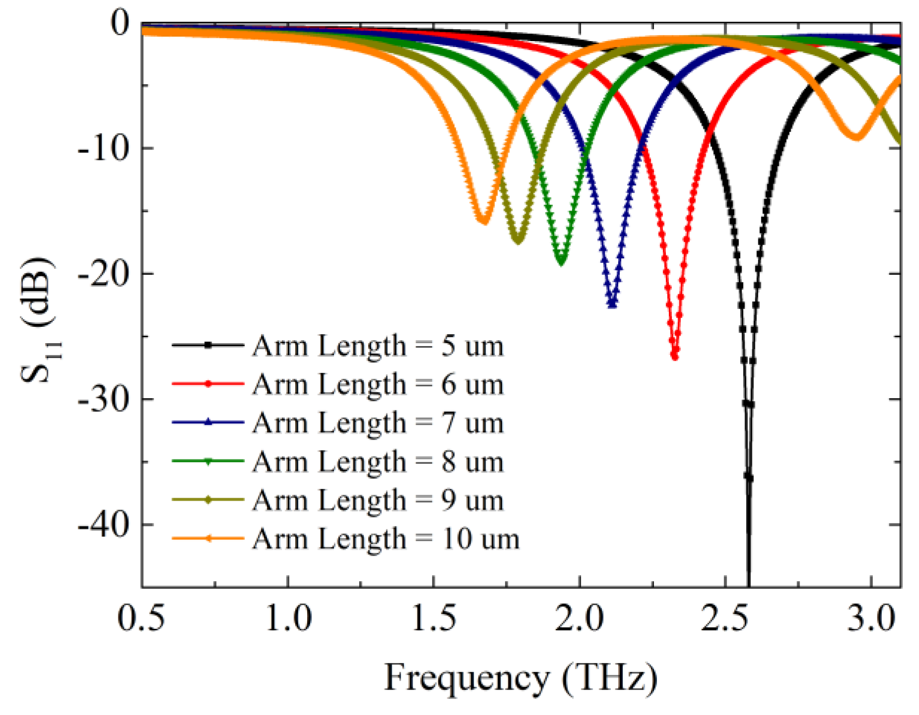
The bowtie antenna is a quasi-dipole antenna, which can be controlled to show different resonance points with changing arm length. In this part, the antenna arm lengths ranging from 5 to 10 µm were considered and results were obtained as shown in Figure 3, Figure 4 and Figure 5. We only demonstrate the S-parameter curves when the chemical potential was 0.2 eV, as shown in Figure 3. As the arm length increased, the resonance point shifted to lower frequencies. At the same time, due to the impedance variation resulting from the arm length change, the resonance performances became worse, from −48 dB to −16 dB. The S-parameters based on other chemical potential levels showed similar trends, which are not shown in this part.
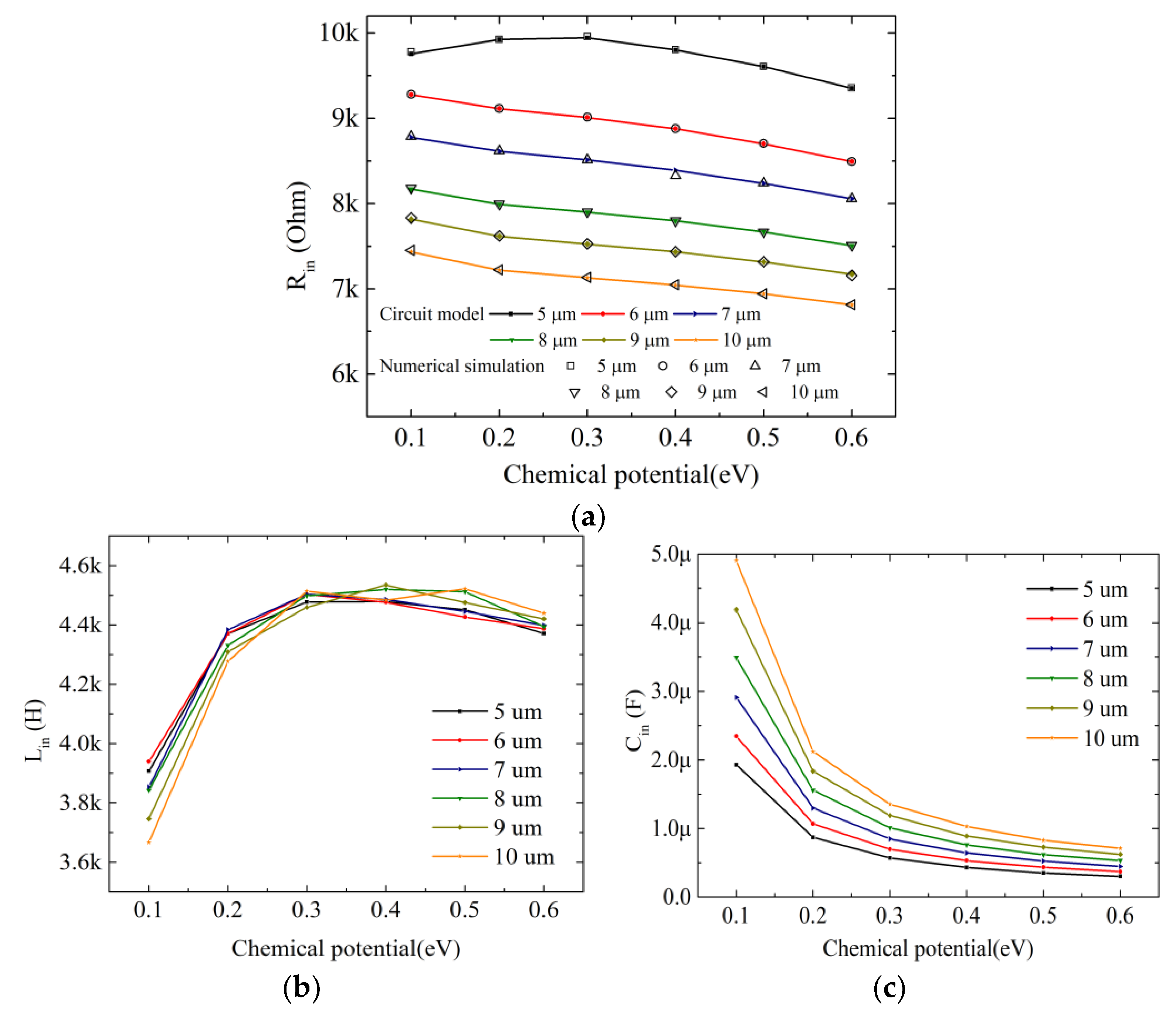
Using the equivalent circuit model proposed in this paper, the calculated coupling coefficient β, quality factor Q0, as well as the Rin, Lin, and Cin parameters are also shown for several arm lengths with increasing energy levels in Figure 4a,b and Figure 5a–c, respectively. As can be seen in Figure 4, for longer arm length, the graphene-based bowtie antenna tended to show a large β value and a smaller Q0, which suggests that input impedance shrinks whilst impedance bandwidth decreases. Also, the β showed a relatively gentle rising comparing to the curves of the quality factor, which indicates chemical potential mainly affects the antenna resonance frequency but not the bandwidth. In Figure 5a, the input resistance Rin decreased as the chemical potential increased from 0.1 to 0.6 eV, and so was the loss on the antenna. When μc = 0.3 eV and the arm length was 5 µm, Rin was close to the source impedance. The arm length of the graphene antenna is related to the SPP wavelength at working frequency. The increasing arm length comes with a reduced impedance. It is noted that the proposed model is validated by comparing to the impedance values calculated by the numerical method in CST. The impedance values from CST were also calculated from S parameters, but they were based on the full-wave numerical algorithm. It is shown that there is a good agreement between the two methods. As shown in Figure 5b, from the perspective of chemical potential, Lin increased as the chemical potential improved, and so did the magnetic energy in the antenna. However, in Figure 5c, Cin shows a different trend when chemical potential increased from 0.1 eV to 0.6 eV, and the electric energy stored at the antenna saw a decline. The equation 1/(ωCin) = ωLin, defines the resonance frequency of this circuit, which is consistent with the curves in Figure 5. At the resonance frequency, the input resistance Rin dominates, and the imaginary part of impedance should be zero. Also, it should be a larger Lin if there is a very small Cin. From the perspective of arm length, Lin and Cin showed different trends as well. With the arm length going up, the magnetic energy stored in the antenna was enriched but the electric one reduced.
4.3. Relaxation Time
The relaxation time of graphene is one of the most fundamental quantities, which is related to the electron scattering rate and the Fermi energy level of graphene. In this part, we analyze the antenna performance and equivalent circuit parameters with several typical and widely used relaxation time values, from 0.1 ps [12], 0.2 ps [33], to 0.5 ps [24,34]. The listed values were carefully chosen to be approximately the same as the realistic values measured in experimental work. It is noted that the larger values are not considered in this work since the graphene with large relaxation time tends to demonstrate higher impedance values, which would result in mismatching and low efficiency of the proposed antenna in this work.
Figure 6 demonstrates the reflection coefficients versus frequency with graphene relaxation time varying from 0.1 ps to 0.5 ps. The chemical potential level of 0.2 eV was chosen to address the impact from the variation of the relaxation time. The S-parameter curves based on other chemical potential levels are expectable and not shown here. It can be seen in Figure 6 that the antenna with longer relaxation time tended to show a sharper resonance. The magnitudes of the resonance curves of relaxation time 0.1 ps and 0.2 ps were both less than 10 dB, which indicates the impedance mismatching in these two cases.
The equivalent circuit parameters were extracted from the simulated S-parameters, as shown in Figure 7 and Figure 8. The coupling coefficients based on different relaxation time values slightly went up, except for the results obtained with the relaxation time of 0.1 ps. The relaxation time 0.1 ps for the proposed graphene antenna was not large enough to drive the antenna. On the contrary, the graphene bowtie antenna based on 0.5 ps relaxation time worked well, as shown in Figure 7.
In Figure 7, the coupling coefficient and the coupled quality factor curves are presented for various relaxation time values. At the relaxation time of 0.1 ps, the β shows a distinct trend, increasing from approximately 2 to more than 9, which was larger than other curves. The quality factor at relaxation time of 0.1 ps, shows a consistent trend with the coupling coefficient. The quality factor value was much lower than the ones with other relaxation time values, which indicates a broader working bandwidth. However, since the antenna barely resonates with relaxation time of 0.1 ps, as shown in Figure 5, the large quality factor does not mean this antenna would behave better than others.
The RLC parameters were also extracted from the equivalent circuit model, as depicted in Figure 8. The input resistances of the proposed antennas showed slight downward trends with all evaluated relaxation times. However, at the relaxation time of 0.5 ps, the graphene antennas with energy level of 0.2 and 0.3 eV demonstrated larger input resistance values (close to 10 kΩ). Moreover, the input resistance increased with relaxation time ranging from 0.1 ps to 0.5 ps. This is consistent with the curves in Figure 7; the graphene antenna with relaxation time of 0.5 ps showed better resonance performance because the input impedance of this antenna matched well with the source impedance of 10 kiloohms. All the designed points were validated by the numerical results obtained from the full-wave simulation solver. The analytical results and the numerical results agree well with each other with different chemical potential levels and relaxation time values.
The curves in Figure 8b suggest that the stored magnetic energy remains with the chemical potential variation while the relaxation time has a significant impact on the magnetic energy of the graphene bowtie antenna. The electric energy is related to the Cin of the extracted circuit model. The antenna with high relaxation time shows relatively low electric energy storage. It is noted that the max value of the Cin was only around 16 µF, which is negligible compared to the Lin values. As a result, the graphene antenna shows more of an inductive nature than a capacitive one.
4.4. Substrate Thickness
The substrate thickness in this paper is selected as 90 nm since this is the value that can maximize the visibility of graphene paved on the quartz substrate [25]. In this part, we also investigate the impacts from the benchmark thickness, 300 nm, and the other typical values, 200 nm and 500 nm. It should be noted that the relaxation time was set as 0.5 ps throughout this part.
The frequency responses of the proposed graphene-based bowtie antenna are presented in Figure 9 with several selected substrate thickness values. Based on the 90-nm-thick substrate, the antenna displayed sharper resonance performance than those with thicker substrates. With such wild change of the substrate thickness, the antenna still worked well to resonate below −10 dB. It should be noted that the resonance points of the antennas demonstrated a shift towards the lower frequencies. As the substrate thickness increases, the fringing fields increase accordingly. This results in a longer effective electrical length of the antenna. In addition, the dispersion relationship of the SPP waves on the graphene sheet can be affected by the substrate thickness, as described in Equation (3). With the very thin substrate and the wild change (from 90 nm to 500 nm) of the substrate thickness, the SPP wavelength would become longer and then the working frequency would shift a lot to the lower frequencies.
As can be observed in Figure 10a, the coupling coefficient, similarly, showed gentle trends with the rise of chemical potential of the graphene-based bowtie antenna. Also, the coupling coefficient went up from approximately 1 to 1.5 when the antenna rested on a thicker substrate with thickness up to 500 nm. In Figure 10b, the quality factor increased with chemical potential rises, while the antenna with a thicker substrate tended to demonstrate higher quality values, which would lower the bandwidth of the antenna.
Similar to the results in the previous subsections, the RLC model is presented with the parameters of interest. In Figure 11a, the input resistance values from the proposed equivalent circuit model as well as the numerical simulation results are demonstrated with different substrate thickness values. The impact from the chemical potential has been well discussed in the above texts. We will focus on the influence brought by the various antenna substrate thickness values in this subsection. As observed in Figure 11a, the graphene-based bowtie antenna with 90-nm-thick substrate demonstrated higher input impedance than other antennas, reaching 10 kΩ. As a result, the higher input impedance led to better matching and sharper resonance.
In Figure 11a,b, the Lin increased with both chemical potential and substrate thickness rising. The electric capacity of the antenna at the resonance point was at a very low level, only several microfarads. The substrate would trap the energy radiated from the antenna, which would lower the antenna efficiency. In this case, with the 500-nm-thick substrate, the antenna displayed a more inductive manner than the one with a thinner substrate. The stored magnetic energy dominated the antenna, which is consistent with the previous analysis. With a thicker substrate, the antenna showed higher capacity, as seen in Figure 11c. The substrate thickness should be carefully chosen to make sure that the antenna resonates well at the desired frequency band. For a certain substrate thickness, we should carefully adjust the antenna dimensions, so the antenna could have a better impedance matching with the source, which leads to relatively low S11 values.
5. Conclusions
In summary, an equivalent resonance circuit model with R, L, and C connected in series has been proposed to describe the graphene-based THz bowtie antenna for the insight of the resonance behavior of the graphene antenna. Several significant parameters, chemical potential, the antenna arm length, relaxation time, and substrate thickness, are considered in the modeling and analysis. By using the equivalent circuit modeling, it has been shown that the R values decrease as the chemical potential and the arm length increase. Also, C values show a similar trend with tuning the energy level. Antenna dimension also shows influence on the extracted circuit parameters. L and C values remain a balance to keep a very small value of the imaginary part of input impedance. This indicates physically that the high energy level tends to reduce the loss resistance and the increasing arm length tends to drain the magnetic energy stored in this set of antennas. Electric energy varies with magnetic energy to keep a balance. The rise of relaxation time leads to higher input resistance, which would influence the resonance performance. The substrate thickness affects both the resonance frequency and magnitude. The graphene-based bowtie antenna shows more an inductive property than a capacitive one. The proposed model is validated by the numerical results. This work sheds light on the graphene-based bowtie antenna design and paves the way for further investigation and potential applications.
Author Contributions
B.Z. performed the simulation and wrote the paper. J.Z. and Z.P.W. proposed the idea and C.L., J.Z., D.H. and Z.P.W. helped with the results discussion and paper revision.
Funding
This research was funded by the Fundamental Research Funds for the Central Universities, grant number WUT: 2017IB015.
Conflicts of Interest
The authors declare no conflict of interest.
References
- Akyildiz, I.F.; Jornet, J.M.; Han, C. Terahertz band: Next frontier for wireless communications. Phys. Commun. 2014, 12, 16–32. [Google Scholar] [CrossRef]
- Akyildiz, I.F.; Miquel, J. Realizing Ultra-Massive MIMO (1024 × 1024) Communication in the (0.06–10) Terahertz band. Nano Commun. Netw. 2016, 8, 46–54. [Google Scholar] [CrossRef]
- Geim, A.K.; Novoselov, K.S. The rise of graphene. Nat. Mater. 2007, 6, 183–191. [Google Scholar] [CrossRef] [PubMed]
- Hanson, G.W. Dyadic green’s functions for an anisotropic, non-local model of biased graphene. IEEE Trans. Antennas Propag. 2008, 56, 747–757. [Google Scholar] [CrossRef]
- Bablich, A.; Kataria, S.; Lemme, M. Graphene and Two-Dimensional Materials for Optoelectronic Applications. Electronics 2016, 5, 13. [Google Scholar] [CrossRef]
- Dragoman, M.; Muller, A.A.; Dragoman, D.; Coccetti, F.; Plana, R. Terahertz antenna based on graphene. J. Appl. Phys. 2010, 107, 104313. [Google Scholar] [CrossRef]
- Vakil, A.; Engheta, N. Transformation Optics Using Graphene. Science. 2011, 332, 1291–1294. [Google Scholar] [CrossRef] [PubMed]
- Jablan, M.; Buljan, H.; Soljačić, M. Plasmonics in graphene at infrared frequencies. Phys. Rev. B 2009, 80, 245435. [Google Scholar] [CrossRef]
- Llatser, I.; Kremers, C.; Cabellos-Aparicio, A.; Jornet, J.M.; Alarcón, E.; Chigrin, D.N. Graphene-based nano-patch antenna for terahertz radiation. Photonics Nanostruct. Fundam. Appl. 2012, 10, 353–358. [Google Scholar] [CrossRef] [Green Version]
- Tamagnone, M.; Gómez-Díaz, J.S.; Mosig, J.R.; Perruisseau-Carrier, J. Reconfigurable terahertz plasmonic antenna concept using a graphene stack. Appl. Phys. Lett. 2012, 101, 214102. [Google Scholar] [CrossRef] [Green Version]
- Wang, X.; Zhao, W.; Hu, J.; Yin, W. Reconfigurable Terahertz Leaky-Wave Antenna Using Graphene-based High-impedance Surface. IEEE Trans. Nanotechnol. 2015, 14, 62–69. [Google Scholar] [CrossRef]
- Llatser, I.; Kremers, C.; Chigrin, D.N.; Jornet, J.M.; Lemme, M.C.; Cabellos-Aparicio, A.; Alarcon, E. Characterization of graphene-based nano-antennas in the terahertz band. Radioengineering 2012, 21, 946–953. [Google Scholar]
- Amanatiadis, S.A.; Karamanos, T.D.; Kantartzis, N.V. Radiation Efficiency Enhancement of Graphene THz Antennas Utilizing Metamaterial Substrates. IEEE Antennas Wirel. Propag. Lett. 2017, 16, 2054–2057. [Google Scholar] [CrossRef]
- Hosseininejad, S.E.; Neshat, M.; Faraji-Dana, R.; Lemme, M.C.; Haring Bolívar, P.; Cabellos-Aparicio, A.; Alarcón, E.; Abadal, S. Reconfigurable THz Plasmonic Antenna Based on Few-layer Graphene With High Radiation Efficiency. Nanomaterials 2018, 8, 577. [Google Scholar] [CrossRef] [PubMed]
- Correas-Serrano, D.; Gomez-Diaz, J.S. Graphene-based Antennas for Terahertz Systems: A Review. arXiv, 2017; arXiv:1704.00371. [Google Scholar]
- Li, L.; Liang, C.-H. Analysis of Resonance and Quality Factor of Antenna and Scattering Systems Using Complex Frequency Method Combined With Model-Based Parameter Estimation. Prog. Electromagn. Res. 2004, 46, 165–188. [Google Scholar] [CrossRef]
- Majeed, F.; Shahpari, M.; Thiel, D.V. Pole-zero analysis and wavelength scaling of carbon nanotube antennas. Int. J. RF Microw. Comput.-Aided Eng. 2017, 27, e21103. [Google Scholar] [CrossRef]
- Tamagnone, M.; Perruisseau-Carrier, J. Predicting Input Impedance and Efficiency of Graphene Reconfigurable Dipoles Using a Simple Circuit Model. IEEE Antennas Wirel. Propag. Lett. 2014, 13, 313–316. [Google Scholar] [CrossRef] [Green Version]
- Cao, Y.S.; Jiang, L.J.; Ruehli, A.E. An Equivalent Circuit Model for Graphene-Based Terahertz Antenna Using the PEEC Method. IEEE Trans. Antennas Propag. 2016, 64, 1385–1393. [Google Scholar] [CrossRef]
- Lovat, G. Equivalent circuit for electromagnetic interaction and transmission through graphene sheets. IEEE Trans. Electromagn. Compat. 2012, 54, 101–109. [Google Scholar] [CrossRef]
- Wu, Z.; Davis, L.E. Automation-orientated techniques for quality-factor measurement: Of high-Tc superconducting resonators. IEE Proc. Sci. Meas. Technol. 1994, 141, 527–530. [Google Scholar] [CrossRef]
- Hanson, G.W. Dyadic Green’s functions and guided surface waves for a surface conductivity model of graphene. J. Appl. Phys. 2008, 103, 064302. [Google Scholar] [CrossRef] [Green Version]
- Locatelli, A.; Town, G.E.; De Angelis, C. Graphene-Based Terahertz Waveguide Modulators. IEEE Trans. Terahertz Sci. Technol. 2015, 5, 351–357. [Google Scholar] [CrossRef]
- Zakrajsek, L.; Einarsson, E.; Thawdar, N.; Medley, M.; Jornet, J.M. Lithographically Defined Plasmonic Graphene Antennas for Terahertz-Band Communication. IEEE Antennas Wirel. Propag. Lett. 2016, 15, 1553–1556. [Google Scholar] [CrossRef]
- Blake, P.; Hill, E.W.; Castro Neto, A.H.; Novoselov, K.S.; Jiang, D.; Yang, R.; Booth, T.J.; Geim, A.K. Making graphene visible. Appl. Phys. Lett. 2007, 91, 063124. [Google Scholar] [CrossRef] [Green Version]
- Tamagnone, M.; Gómez-Díaz, J.S.; Mosig, J.R.; Perruisseau-Carrier, J. Analysis and design of terahertz antennas based on plasmonic resonant graphene sheets. J. Appl. Phys. 2012, 112, 114915. [Google Scholar] [CrossRef] [Green Version]
- Gregory, I.S.; Baker, C.; Tribe, W.R.; Bradley, I.V.; Evans, M.J.; Linfield, E.H.; Davies, A.G.; Missous, M. Optimization of photomixers and antennas for continuous-wave terahertz emission. IEEE J. Quantum Electron. 2005, 41, 717–728. [Google Scholar] [CrossRef] [Green Version]
- Duffy, S.M.; Verghese, S.; McIntosh, K.A.; Jackson, A.; Gossard, A.C.; Matsuura, S. Accurate modeling of dual dipole and slot elements used with photomixers for coherent terahertz output power. IEEE Trans. Microw. Theory Tech. 2001, 49, 1032–1038. [Google Scholar] [CrossRef]
- Cabellos, A.; Llátser, I.; Alarcón, E. Use of THz Photoconductive Sources to Characterize Graphene RF Plasmonic Antennas. IEEE Trans. Nanotechnol. 2015, 14, 390–396. [Google Scholar] [CrossRef]
- Yaghjian, A.D.; Best, S.R. Impedance, bandwidth, and Q of antennas. IEEE Trans. Antennas Propag. 2005, 53, 1298–1324. [Google Scholar] [CrossRef] [Green Version]
- Shahpari, M.; Thiel, D.V.; Lewis, A. An investigation into the gustafsson limit for small planar antennas using optimization. IEEE Trans. Antennas Propag. 2014, 62, 950–955. [Google Scholar] [CrossRef]
- Gilbert, R.A.; Volakis, J. Antenna Engineering Handbook, 4th ed.; John Wiley & Sons, Inc.: Hoboken, NJ, USA, 2007; ISBN 9780071475747. [Google Scholar]
- Kim, J.Y.; Lee, C.; Bae, S.; Kim, K.S.; Hong, B.H.; Choi, E.J. Far-infrared study of substrate-effect on large scale graphene. Appl. Phys. Lett. 2011, 98, 2009–2012. [Google Scholar] [CrossRef]
- Zouaghi, W.; Voß, D.; Gorath, M.; Nicoloso, N.; Roskos, H.G. How good would the conductivity of graphene have to be to make single-layer-graphene metamaterials for terahertz frequencies feasible? Carbon. 2015, 94, 301–308. [Google Scholar] [CrossRef]
Figure 1.
(a) The schematic of the graphene-based bowtie antenna; (b) the corresponding equivalent resonant circuit.
Figure 1.
(a) The schematic of the graphene-based bowtie antenna; (b) the corresponding equivalent resonant circuit.

Figure 2.
Simulated reflection coefficient with chemical potential levels from 0.1 eV to 0.6 eV. The relaxation time is 0.5 ps and the temperature is 300 K.
Figure 2.
Simulated reflection coefficient with chemical potential levels from 0.1 eV to 0.6 eV. The relaxation time is 0.5 ps and the temperature is 300 K.
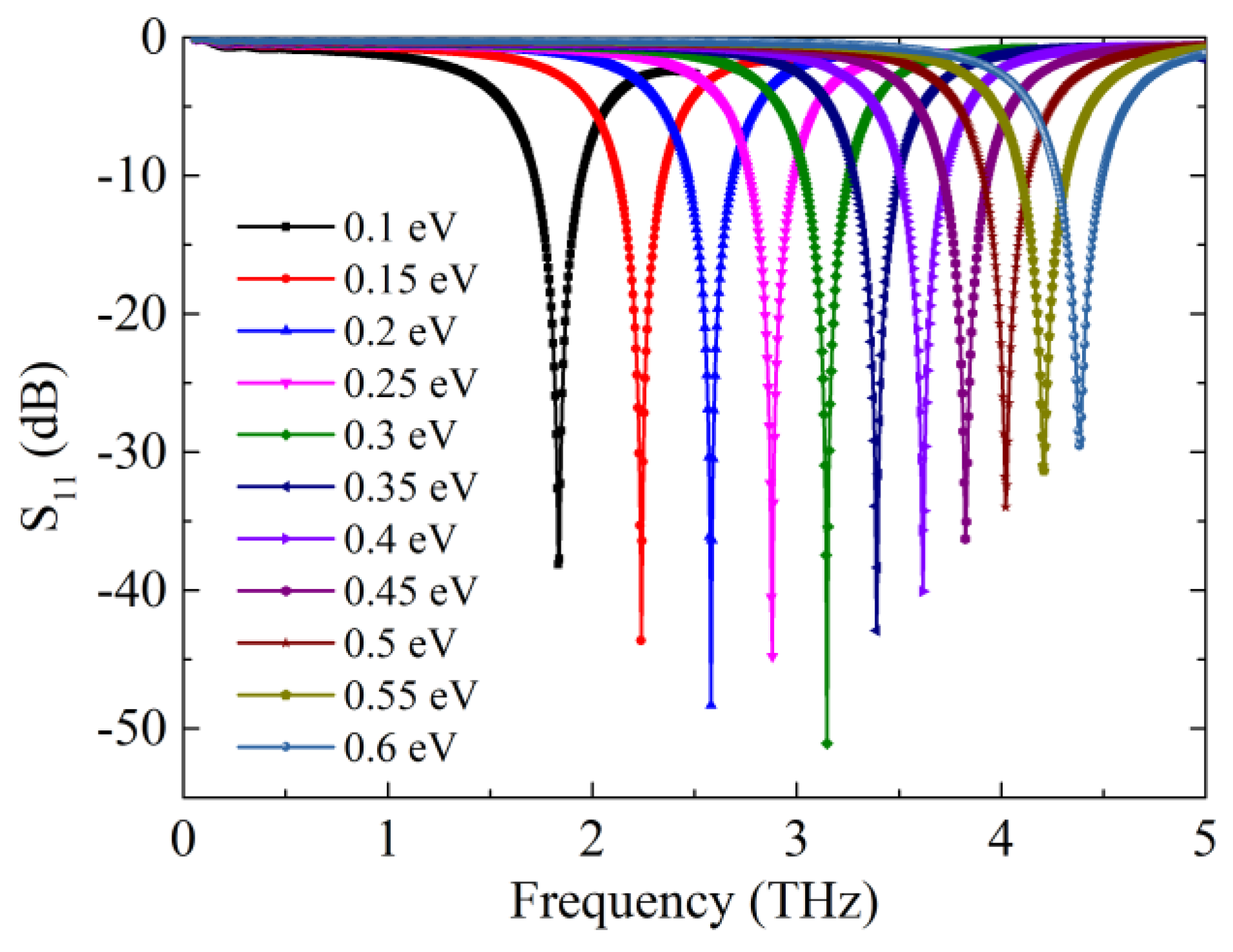
Figure 3.
Simulated reflection coefficient with arm length ranging from 5 µm to 10 µm. The relaxation time is 0.5 ps and the temperature is 300 K.
Figure 3.
Simulated reflection coefficient with arm length ranging from 5 µm to 10 µm. The relaxation time is 0.5 ps and the temperature is 300 K.

Figure 4.
Calculated circuit parameter results versus chemical potential with arm length 5–10 µm. (a) β and (b) Q0 curves with the arm length ranging from 5 µm to 10 µm over different chemical potentials.
Figure 4.
Calculated circuit parameter results versus chemical potential with arm length 5–10 µm. (a) β and (b) Q0 curves with the arm length ranging from 5 µm to 10 µm over different chemical potentials.

Figure 5.
Equivalent circuit parameters. (a) Rin, (b) Lin, and (c) Cin of the equivalent circuit against chemical potential with different arm lengths. The solid lines are the results from the equivalent circuit model and the scatter denotes the numerical data. The relaxation time is 0.5 ps and the temperature is 300 K.

Figure 6.
Simulated reflection coefficient with different relaxation times, 0.1 ps, 0.2 ps, 0.3 ps, 0.4 ps, and 0.5 ps. The arm length is 5 µm and the temperature is 300 K.
Figure 6.
Simulated reflection coefficient with different relaxation times, 0.1 ps, 0.2 ps, 0.3 ps, 0.4 ps, and 0.5 ps. The arm length is 5 µm and the temperature is 300 K.
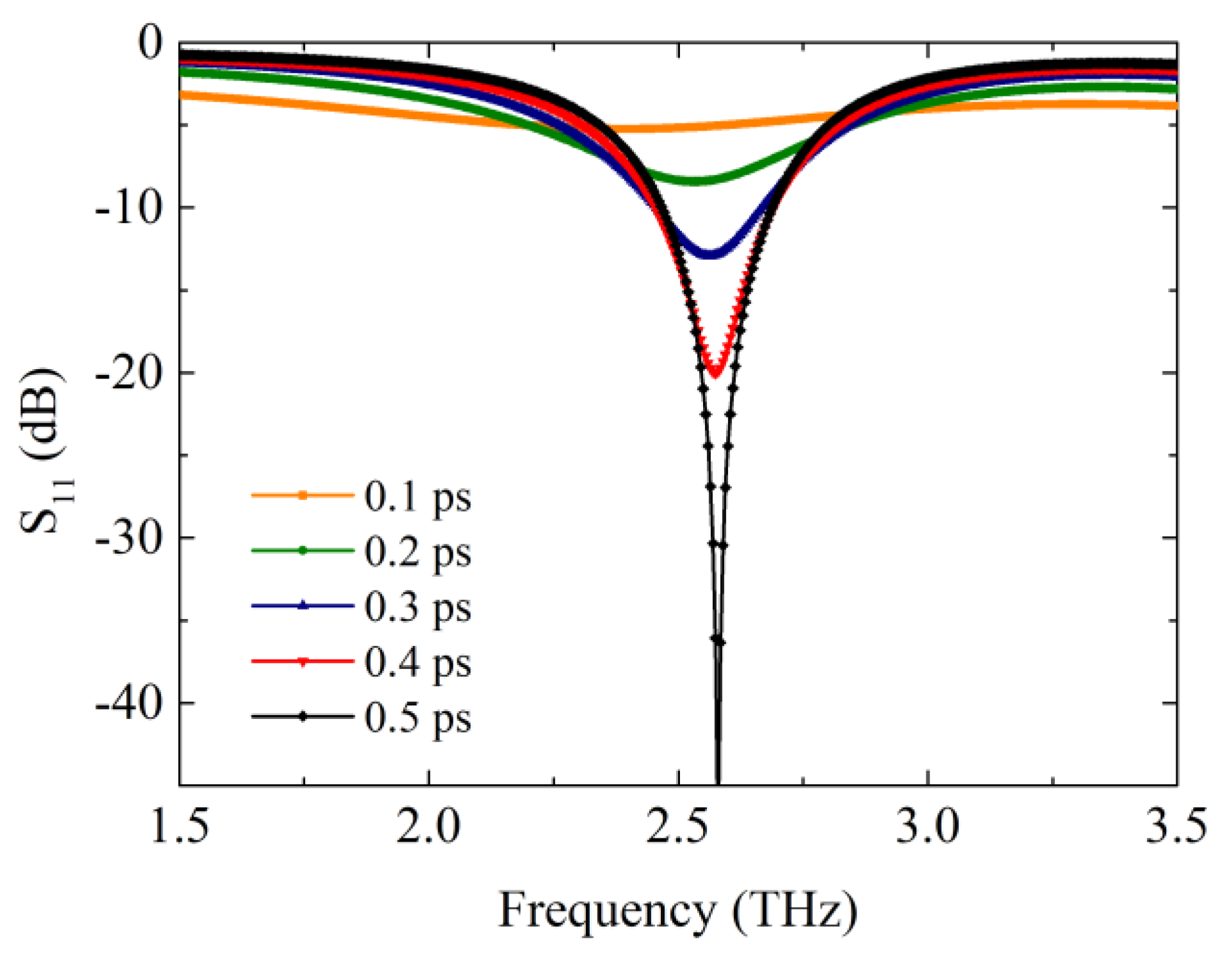
Figure 7.
The calculated circuit parameter results versus chemical potential with different relaxation times. (a) β and (b) Q0 curves with the graphene relaxation time from 0.1 ps to 0.5 ps over different chemical potentials.
Figure 7.
The calculated circuit parameter results versus chemical potential with different relaxation times. (a) β and (b) Q0 curves with the graphene relaxation time from 0.1 ps to 0.5 ps over different chemical potentials.

Figure 8.
Equivalent circuit parameters. (a) Rin, (b) Lin, and (c) Cin of the equivalent circuit against chemical potential with different relaxation times: 0.1 ps, 0.2 ps, 0.3 ps, 0.4 ps, and 0.5 ps.
Figure 8.
Equivalent circuit parameters. (a) Rin, (b) Lin, and (c) Cin of the equivalent circuit against chemical potential with different relaxation times: 0.1 ps, 0.2 ps, 0.3 ps, 0.4 ps, and 0.5 ps.

Figure 9.
Simulated reflection coefficient with different substrate thickness values, 90 nm, 200 nm, 300 nm, and 500 nm. The arm length is 5 µm, the temperature is 300 K, and the relaxation time is 0.5 ps.
Figure 9.
Simulated reflection coefficient with different substrate thickness values, 90 nm, 200 nm, 300 nm, and 500 nm. The arm length is 5 µm, the temperature is 300 K, and the relaxation time is 0.5 ps.
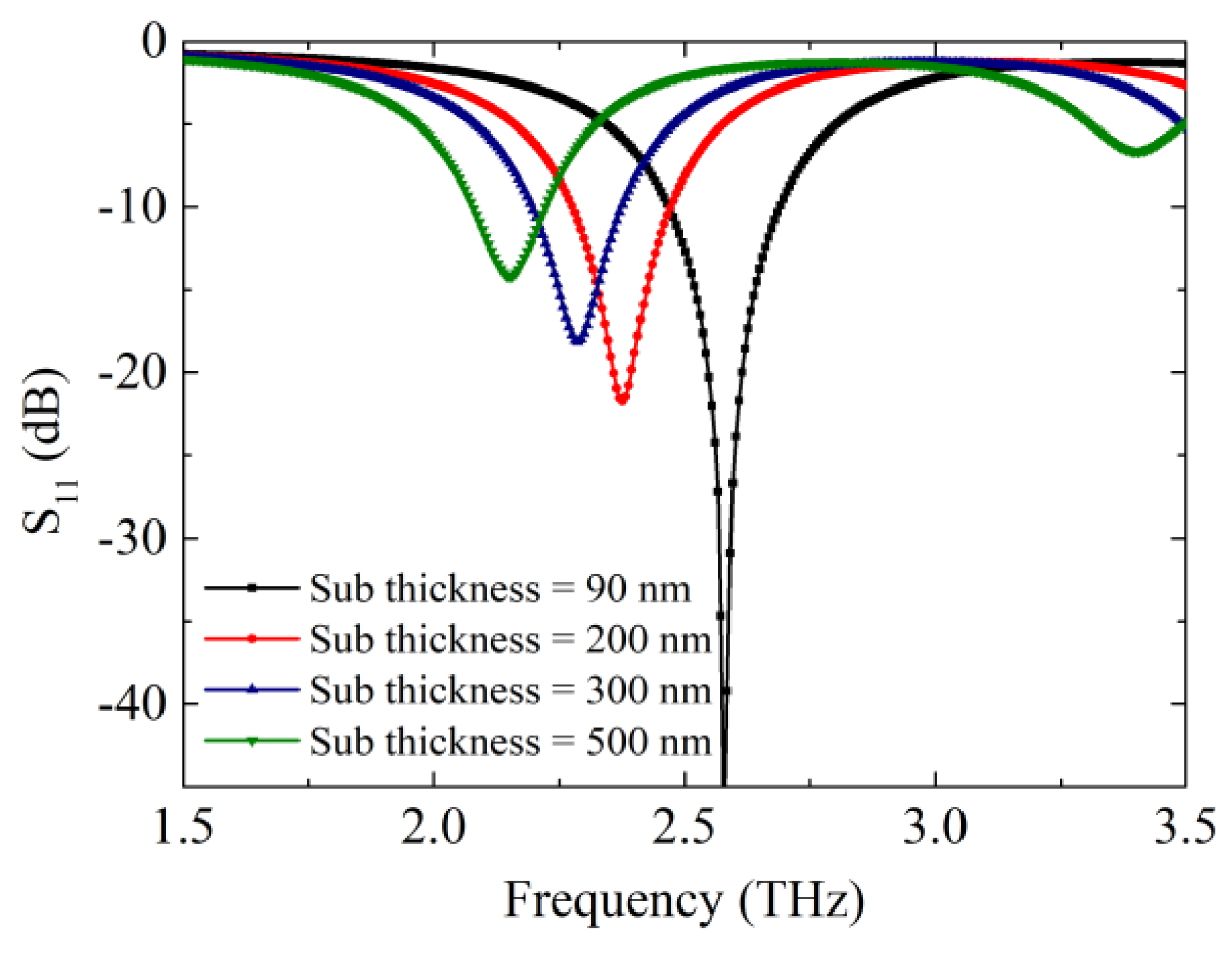
Figure 10.
The calculated circuit parameter results versus chemical potential. (a) β and (b) Q0 curves with different substrate thickness values, 90 nm, 200 nm, 300 nm, and 500 nm. The relaxation time is set as 0.5 ps, the arm length is 5 µm and the temperature is 300 K.
Figure 10.
The calculated circuit parameter results versus chemical potential. (a) β and (b) Q0 curves with different substrate thickness values, 90 nm, 200 nm, 300 nm, and 500 nm. The relaxation time is set as 0.5 ps, the arm length is 5 µm and the temperature is 300 K.
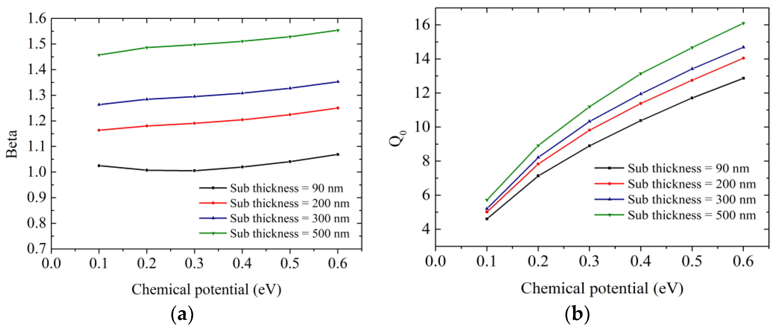
Figure 11.
Equivalent circuit model parameters over chemical potentials. (a) Rin, (b) Lin, and (c) Cin of the equivalent circuit against chemical potential with different substrate thickness values, 90 nm, 200 nm, 300 nm, and 500 nm. The relaxation time is 0.5 ps, the temperature is 300 K, and the arm length is 5 µm.


Table 1.
The simulated data with chemical potential ranging from 0.1 eV to 0.6 eV. The relaxation time is set as 0.5 ps, the arm length is 5 µm, the thickness of the substrate is 90 nm.
Table 1.
The simulated data with chemical potential ranging from 0.1 eV to 0.6 eV. The relaxation time is set as 0.5 ps, the arm length is 5 µm, the thickness of the substrate is 90 nm.
| μc/eV | f0/THz | S11(f0)/dB | Rin/Ω | Lin/H | Cin/F | Xin/Ω | β | Qa | Q0 | Rin,CST/Ω |
|---|---|---|---|---|---|---|---|---|---|---|
| 0.1 | 1.8335 | −38.125 | 9754.9 | 3907.3 | 1.93 × 10⁻⁶ | 0.00 | 1.0251 | 2.2734 | 4.6143 | 9781 |
| 0.15 | 2.2385 | −43.636 | 9869.3 | 4208.9 | 1.20 × 10⁻⁶ | 0 | 1.0132 | 2.9725 | 5.9983 | 9871 |
| 0.2 | 2.5794 | −48.305 | 9923.4 | 4370.5 | 8.71 × 10⁻⁷ | 0.00 | 1.0077 | 3.5468 | 7.1378 | 9925 |
| 0.25 | 2.8807 | −44.76 | 9885 | 4406.6 | 6.93 × 10⁻⁷ | −1.46 × 10⁻¹¹ | 1.0116 | 4.0017 | 8.0688 | 9981 |
| 0.3 | 3.1475 | −51.075 | 9944.3 | 4477 | 5.71 × 10⁻⁷ | 0 | 1.0056 | 4.4288 | 8.9035 | 9958 |
| 0.35 | 3.3896 | −42.893 | 9857.7 | 4501.7 | 4.90 × 10⁻⁷ | 0.00 | 1.0144 | 4.8169 | 9.7259 | 9956.23 |
| 0.4 | 3.6168 | −40.06 | 9803.3 | 4478.4 | 4.32 × 10⁻⁷ | −1.46 × 10⁻¹¹ | 1.0201 | 5.1274 | 10.381 | 9805.3 |
| 0.45 | 3.8243 | −36.28 | 9697.7 | 4490.5 | 3.86 × 10⁻⁷ | −1.46 × 10⁻¹¹ | 1.0312 | 5.4662 | 11.126 | 9711.14 |
| 0.5 | 4.0219 | −33.968 | 9607.3 | 4451.6 | 3.52 × 10⁻⁷ | 0.00 | 1.0409 | 5.7259 | 11.709 | 9607.7 |
| 0.55 | 4.2096 | −31.359 | 9473.4 | 4380.1 | 3.26 × 10⁻⁷ | −1.46 × 10⁻¹¹ | 1.0556 | 5.9395 | 12.229 | 9480.8 |
| 0.6 | 4.3825 | −29.526 | 9353.7 | 4371.1 | 3.02 × 10⁻⁷ | −1.46 × 10⁻¹¹ | 1.0691 | 6.2112 | 12.868 | 9355 |
© 2018 by the authors. Licensee MDPI, Basel, Switzerland. This article is an open access article distributed under the terms and conditions of the Creative Commons Attribution (CC BY) license (http://creativecommons.org/licenses/by/4.0/).
Share and Cite
MDPI and ACS Style
Zhang, B.; Zhang, J.; Liu, C.; Wu, Z.P.; He, D. Equivalent Resonant Circuit Modeling of a Graphene-Based Bowtie Antenna. Electronics 2018, 7, 285. https://doi.org/10.3390/electronics7110285
AMA Style
Zhang B, Zhang J, Liu C, Wu ZP, He D. Equivalent Resonant Circuit Modeling of a Graphene-Based Bowtie Antenna. Electronics. 2018; 7(11):285. https://doi.org/10.3390/electronics7110285
Chicago/Turabian StyleZhang, Bin, Jingwei Zhang, Chengguo Liu, Zhi P. Wu, and Daping He. 2018. "Equivalent Resonant Circuit Modeling of a Graphene-Based Bowtie Antenna" Electronics 7, no. 11: 285. https://doi.org/10.3390/electronics7110285
Note that from the first issue of 2016, this journal uses article numbers instead of page numbers. See further details here.