Analytical Approach in the Development of RF MEMS Switches


1
Department of Electronic Apparatuses Design, Southern Federal University, Taganrog 347929, Russia
2
Taganrog Scientific Research Institute of Communication, Taganrog 347913, Russia
*
Author to whom correspondence should be addressed.
Electronics 2018, 7(12), 415; https://doi.org/10.3390/electronics7120415
Submission received: 22 November 2018
/
Revised: 6 December 2018
/
Accepted: 6 December 2018
/
Published: 10 December 2018
(This article belongs to the Special Issue Advanced Technology Related to Radar Signal, Imaging, and Radar Cross-Section Measurement)
Abstract
:Currently, the technology of microelectromechanical systems is widely used in the development of high-frequency and ultrahigh-frequency devices. The most important requirements for modern and advanced devices of the ultra-high-frequency range are the reduction of weight and size characteristics, power consumption with an increase in their functionality, operating frequency and level of integration. Radio frequency microelectromechanical switches are developed using the technology of the manufacture of CMOS-integrated circuits. Integrated radio frequency control circuits require low control voltages, the high ratio of losses to the isolation in the open and closed condition, high performance and reliability. This review is devoted to the analytical approach based on the knowledge of materials, basic performance indices and mechanisms of failure, which can be used in the development of radio-frequency microelectromechanical switches.
1. Introduction
Radio frequency (RF) electronics of high-frequency (HF) and ultra-high-frequency (UHF) microwave electronics have always needed switches that make low losses in the open state and provide high isolation in a closed state with high permissible signal power and low control power. The first switches fully meet the requirements of steel electromagnetic relays. After many years of improvement modern RF relays provide low on signal loss and high isolation in the off state, but they have such disadvantages as large overall dimensions, high cost and limited resource (from hundreds of thousands to tens of millions of cycles).
The switch on PIN-diodes and field-effect transistors based on GaAs have a number of advantages over the RF relay, consisting in high speed operation, small size and weight, as well as low-power control. However, they introduce higher losses into the microwave transmission line and, therefore, cannot replace electromechanical switches in a number of applications. Further research led to the development of RF switches based on microelectromechanical systems (MEMS), which combined some of the advantages of semiconductor and relay devices.
The comparative characteristics of semiconductor switches are based on PIN-diodes and field-effect transistors, MEMS switches and electromechanical switches of the UHF signal [1].
Micromechanical microwave switches were first demonstrated by Petersen as cantilever beams using electrostatic actuation [2].
According to the forecast of MEMS devices market development, published in 2015 in [3], the following areas of MEMS technologies are noted for high growth: pressure sensors, inertial measurement systems, microfluidic devices and systems. Nevertheless, RF MEMS devices have shown a significant growth from 2014 to 2020, which have great market potential and have been declared as one of the main applications of MEMS technologies.
The RF MEMS segment consisting of filters based on volume acoustic waves and switches boost the income level of the entire MEMS area as a whole with estimated revenues in 2022 at 10 billion dollars [4].
Driven by the complexities associated with the move to 5G and the higher number of bands it brings, there is an increasing demand for RF filters in 4G/5G, making RF MEMS the largest-growing MEMS segment. This market will probably soar from US $2.3B in 2017 to US $15B in 2023. Excluding RF MEMS market will grow at 9% over 2018–2023. With RF MEMS the CAGR is 17.5% [4].
With the miniaturization of RF chips and the growing need to improve their functions, the trend towards integration of RF MEMS and CMOS devices for RF applications will only increase.
RF MEMS switches utilize various actuation designs including electromagnetic [5,6,7,8], magnetostatic [9], electrostatic [10], thermal-electric [11] and various structural designs including a rotating transmission line [12], surface micromachined cantilevers [13,14,15,16,17], multiplesupported or membrane based designs [18,19], bulkmicromachined or wafer bonded designs [20,21,22], diamond cantilever and contact [23], polysilicon switch [24], mercury micro-drop contact [25,26] and bistable microrelays [27,28]. All switches designs have their advantages and disadvantages. The micromachined electrostatic switches or relays are the most widely studied devices to date.
RF MEMS switches with electrostatic activation mechanism are characterized by their own power consumption of the order of several mW, which is considerably lower in comparison with other type of RF MEMS switches. Therefore, most of the developed RF MEMS switches have an electrostatic activation mechanism. At the technological level of electrostatic control it does not require the deposition of specific materials, for example, with piezoelectric or ferromagnetic properties which simplifies the manufacturing technology and, therefore, reduces the cost of finished devices.
However, research conducted in the field of RF MEMS switches is largely limited only by the RF characteristics of these devices, although taking into account the interdisciplinary nature of MEMS technologies, it is necessary to take into account the relationship of electrical parameters with the mechanical parameters of MEMS structures. For example, residual stresses in deposited metal layers of RF MEMS switches have a much greater impact on the performance and life expectancy of the device than expected. In addition, the vast majority of RF MEMS switches require large values of control voltage (40–100 V for pull-down voltage and 15–30 V for hold-down voltage, respectively), along with high switching time, which significantly reduces the scope of their application, excluding wireless communication devices, which involve the use of low-voltage power supplies given the growing demand for RF MEMS switches in this area [3,4,29]. In [30] is also shown that the life expectancy of MEMS switches with an electrostatic activation mechanism strongly depends on the magnitude of the applied voltage.
In addition, achieving a high switching speed remains a major limitation; few studies have been devoted to improving the switching speed, except that proposed in [31], by miniaturizing the MEMS switch. In [32], the authors demonstrate the switching time at the level of nanoseconds through the use of the membrane dielectricas as a structural material. It is shown in [33] that the addition of curved sides to miniature elastic suspension elements increases the stiffness coefficient, causing a further increase in the resonance frequency, which leads to a low switching time. Consequently, improving the switching speed has a negative effect on the control voltage. Increasing the stiffness of the elastic suspension elements will inevitably lead to an increase in the value of the control voltage.
In general, our review presents new design solutions and an analytical approach to the development of RF MEMS switches. The analytical approach is based on the knowledge of materials, key performance indices and failure mechanisms of RF MEMS switches, and parametric analysis is based on a mathematical model.
2. Analytical Approach to the Development of RF MEMS Switches of Electrostatic Type
The analytical approach in the development of RF MEMS switches has the following structure, shown in Figure 1.
2.1. The Influence of Switching Characteristics of Switch
RF MEMS switches differ in both the activation mechanism and the principle of switching— resistive and capacitive.
The main criterion in the development of RF MEMS resistive type switches (see Figure 2) is the contact area. Large contact areas have less resistance and, therefore, lower contact temperature. The contact area is determined by the applied force and hardness of the material, as well as its ability to form a surface layer with high-resistance. It is also necessary to take into account the adhesive force in the contact—the cantilever or the switch membrane must be sufficiently strong to overcome the adhesive force after removal of the control voltage [1].
Typically, switches with a resistive switching principle are used in a wide frequency range from 0 to 50 GHz, contact resistance of resistive switch based on gold, as a rule, lies in the range of 0.15–0.4 Ω, contact force on the site is from 80 to 500 µN. However, a feature of resistive switches is the need to supply a sufficiently high control voltage—from 60 to 80 V [13,16,34,35].
RF MEMS switches with capacitive switching principle (see Figure 3) operate by changing the capacitance between the waveguide and the grounded electrode. Typically, switches with capacitive switching principle are used as shunt switches [35] with operating frequencies from 10 to 100 GHz, losses 0.2 dB, isolation from 15 to 35 dB for operating frequencies [37,38,39].
The main advantage of RF MEMS capacitive type switches is the ability to develop switches with low control voltage, since there is no need to make a significant effort to create a contact. However, RF MEMS devices of this type are sensitive to surface roughness and internal stresses in the membrane [38] due to the appearance of an additional air gap, which significantly affects the ratio of capacities in the ON and OFF states. The power handling of RF MEMS switches of the capacitive type does not exceed 7 W, since the current density can exceed the critical value due to the high-resistance of the membrane fastening compared to the switches of resistive type [1].
For the manufacture of high-power handling RF MEMS switches (100 mW and above) more preferred type of contact is the resistive switching principle. This is due to the need to use membranes with a rigid mount for the capacitive switching principle due to the effects of arbitrary operation and high current density, which eliminates their advantages over switches with a resistive switching principle.
For the manufacture of switches of medium and low-power handling (up to 100 mW), switch with capacitive switching principle has an important advantage; the ability to manufacture a switch with low-voltage operation, which allows the use of a single power supply circuit for semiconductor devices and to control the switches.
2.2. Causes of Failure of RF MEMS Switches
For RF MEMS switches with capacitive switching principle at low-power handling (1 mW and below) the main failure mechanism is the electric charge of the dielectric film. The solution to this problem is the use of control voltages with variable polarity [39,40]. For medium-power handling switches (10–100 mW) the main failure mechanisms are related to the electric charge of the dielectric film and failure due to high current density. Problems of failure due to high current density are usually solved by increasing the thickness of the membrane [41,42]. For high-power handling switches the main mechanisms are random tripping and high current density. Random triggering occurs at a voltage in the RF transmission line comparable to the pull-down or return voltage. The solution to this problem is to increase the stiffness of the switch design and control the membrane using separate electrodes [43,44].
For RF MEMS switches with a resistive switching principle at low-power handling (less than 1 mW), the main failure mechanisms are erosion, contact hardening and the formation of dielectric films on the contact. The solution to this problem lies in the selection of materials with the best contact characteristics [45,46]. Medium-power handling switches (10–100 mW) fail due to high contact current density and contact microwelding. This problem is solved by the selection of materials with better contact characteristics [47,48,49,50]. For high-power handling switches (100 mW or more), the main failure mechanism is temperature rise, high current density and microwelding of contacts. This problem is solved by constructive work on cooling the contact area, the selection of materials contact [35,51,52].
2.3. Selection of Structural Material of RF MEMS Switch with Capacitive Switching Principle
Due to the fact that the stiction of the membrane to the pull-down electrode as a consequence of the electric charge of the dielectric film is one of the main problems of the reliability of RF MEMS switches with capacitive switching principle, significant efforts of researchers in this area have been aimed at reducing or completely eliminating this problem. In this regard, the properties of materials play a very important role in preventing stiction.
The choice of structural material depends on the hardness, resistance and complexity of the process. The properties of the materials significantly depend on the conditions and deposition technology of the material. For example, the specific resistance of the deposited metal film is almost twice that of the original material. Pure Au provides the lowest contact resistance and is inert to the formation of oxides, but it has been empirically found that the predominant number of failures are associated with pure Au due to the point destruction of the contact area under repeated efforts. Hence, pure Au is not suitable as a structural material of RF MEMS switches that require a long lifespan. Solid metals, such as tungsten or molybdenum, are capable of processing sufficiently high-frequency signal power and do not exhibit any stiction problems. However, they are more sensitive to oxidation and require a relatively high initial contact force. Thus, tungsten and molybdenum are not suitable as structural material. From the obtained results, it was found that the evaporated aluminum is one of the suitable candidates as a contact material [53].
Such materials as gold, aluminum, platinum, molybdenum, copper, and nickel can be used to make an RF MEMS switch with capacitive switching principle [54,55,56,57].
When choosing the appropriate material, we should address three main performance indexes of the RF MEMS switches with capacitive switching principle: pull-down voltage, the level of RF losses, thermal residual stress. The key material properties are Young’s modulus, Poisson’s ratio, thermal expansion coefficient and thermal conductivity.
The pull-down voltage is determined by Equation (1) [1]:
where k—the coefficient of stiffness of elastic suspension elements; —the value of the air gap between the electrodes; A—the area of electrostatic interaction.
The coefficient of stiffness k depends on the Young’s modulus, thermal residual stress and Poisson’s ratio of the material of the membrane and the elastic suspension elements. Consequently, the pull-down voltage can be optimized by selecting a material with the corresponding above properties.
The second performance index is the RF loss level, which can be reduced by selecting a material with good conductivity. The power dissipated by RF is determined by Equation (2) [56]:
where I, R—the current and the resistance of the membrane.
At the RF signal of high-power (from 100 mW and above), the membrane of the switch design experiences self-heating, which leads to a change in the thermal residual stress, which is determined by Equation (3) [56]:
where —the level of power dissipated by RF; —the thermal resistance.
Thus, as a result of the analysis, as well as on the basis of material selection diagrams [58], it was found that the most suitable candidate as the main structural material is aluminum after gold and copper.
The use of structures with elastic suspension elements in the form of a meander or thin beams allows us to obtain low values of the stiffness coefficient and control voltage, which is often a compromise between reliability and switching speed.
However, capacitive RF MEMS switches with a low coefficient of rigidity of the elastic suspension elements and low values of the control voltage are subject to deformation, curvature or deformation of the edges of the elastic elements, which prevents the formation of an air gap. The solution to this problem is to use the sandwich structure as a material of elastic suspension elements and the membrane. It embodies two materials of a given geometry and scale, as shown in Figure 4, formed in order to provide high strength and bending rigidity at low mass.
The separated surfaces on both sides of the base material increase the moment of inertia of the structure and form a structure that is well resistant to various kinds of deformations and warping [59]. Another major advantage of sandwich structure is that the balanced structure minimizes the thermal-stress-induced upward warpage in the release process [60,61].
As shown in Figure 4, surfaces with a thickness of t take up most of the load, so they must be tough and durable. In this case, it is proposed to use TiN the advantages of which are high hardness, good adhesion and plasticity, high chemical resistance, high wear resistance, resistance to the formation of oxides and high temperature.
In addition, TiN layers prevent the formation of warps, deformations of the edges of elastic suspension elements, which may be present after deposition in the process of manufacturing the structure. In other words, the TiN layers balance the residual stresses in the Al layer that have arisen after the technological processes. Also, TiN is characterized by high-resolution in the process of photolithography, due to good light adsorption.
In the end, the composite material is proposed to use the sandwich structure TiN/Al/TiN, as a material of elastic suspension elements and the membrane.
2.4. Material Properties of the Sandwich Structure
2.5. Mathematical Model of the RF MEMS Switch with Capacitive Switching Principle
The applied bias voltage is generally separated with respect to the RF signal. One way or another, the potential difference is applied between the membrane connected to the ground lines of the coplanar waveguide and the signal line. Under these conditions, an electrostatic force acts on the design of the switch, which is balanced by the elastic force, depending on the stiffness coefficient k of the elastic suspension elements. In theory, the balance exists until the membrane drops 1/3 of the initial air gap. The membrane then collapses onto the pull-down electrode and a lower voltage value is required to hold it in this position.
The dynamics of the switch are also affected by the presence of a medium (usually air or nitrogen during sealing to eliminate the influence of humidity), which introduces its own friction and causes damping and change in the switching speed [63,64,65]. Currently, there are several models that take into account the detailed effect of damping, including the presence of holes in the membrane [1,66,67,68]. In addition, the damping changes the natural oscillation frequency of the membrane.
Another contribution to the movement of the membrane is made by the contact forces of the membrane with respect to the plane of the coplanar waveguide. They are due to the interaction between the two surfaces and the local redistribution of charges. So we should take into account the impact of the forces Van der Waals forces with the effect of the approximation [63,65].
Both last components are important in the case when the membrane is close to the fixed electrode or is in contact with the dielectric film.
However, a phenomenological approach is usually applied, which takes into account the influence of specific most important parameters useful to describe the required mechanical and electrical response.
Equation (5) of the balance of forces acting on the design of the switch has the form:
where z—the displacement of the membrane; —the mass of the membrane determined by the material density , area A and thickness t.
Taking into account the given physical quantities, Equation (5) can be rewritten in Equation (6) in the following form:
where —the electrostatic force as a consequence of the applied potential difference with the capacitance change along the direction of motion z; —the mechanical force due to the rigidity of the elastic suspension elements, the opposite direction of the electrostatic force ; —the nonlinear tensile force of the elastic suspension element [1]; —the damping force due to the action of the medium, which depends on the speed of the membrane and the damping parameter , which in turn is associated with the geometric parameters of the membrane and the viscosity of the medium; —contact forces, which can be divided into Van der Waals and surface forces; the first acts as an attractive and the second as a repulsive, with a possible equilibrium position at a given distance from the fixed electrode [63].
The total capacity according to Figure 3 is calculated using Equation (7):
where —the dielectric constant of vacuum; —the relative permittivity of the dielectric material film.
The derivative of is used to determine the electrostatic force, which is given by Equation (8):
Thus, Equation (6) can be represented in Equation (9):
2.6. Coefficient of Stiffness of Elastic Suspension Elements
Various variants of elastic elements of membrane fastening are known, which are used to reduce the coefficient of elasticity. The most frequently used variants of elastic elements of the membrane suspension are shown in Figure 5.
The resulting value of the stiffness coefficient k of the elastic elements fastening and membrane is determined by Equation (10):
where —the effective stiffness coefficient of the elastic suspension; —the coefficient of residual stresses in elastic suspension defined by Equation (11):
where —the tensile strength; - the Poisson’s ratio; —the width, the thickness, the length of elastic suspension.
The effective stiffness coefficient depends on the type of elastic suspension fastening:
3. Approbation of the Analytically Approach in the Development of RF MEMS Switches
Schematic view of the developed design of the integrated RF MEMS switch is shown in Figure 6a–c.
The available design of an integrated RF MEMS switch contains substrate with a coplanar transmission line located on it, consisting of two grounding lines and a transmission line. Membrane is made in the form of a plate with perforation, located above the dielectric film with air gap between them. The dielectric film is deposited on the surface of the fixed down electrode, which integrated in the transmission line. Membrane is fixed on the anchor areas (1 level) by means of elastic suspensions consisting of elastic beams in the form of a meander. The fixed upper electrode is made in the form of a plate with perforation used to pull-up the membrane. Movable comb structures and two side electrodes are made in the form of comb structures designed to attract the movable comb structures in the case of action on the construction switch of the external acceleration in the negative or positive direction of the X, Y, Z axes, vibrations or stiction of the membrane in the down or up position.
The switch operates as a variable capacitor with two states depending on the position of the membrane. In the neutral position of the membrane, the capacitance between the membrane and the transmission line is small and the signal flows freely to the output of the transmission line. When a control voltage is applied between the membrane and the fixed down electrode, the charge redistribution occurs, which leads to the appearance of an electrostatic force between them, independent of the polarity of the applied voltage. The electrostatic force causes the membrane to fall to a stationary one and since the structure is bent, tensile forces appear in it seeking to return it to its original position. When the applied control voltage reaches the threshold value, the tensile forces cease to balance the electrostatic forces and the membrane drops sharply to the fixed down electrode. In the down position of the membrane the capacitance value increases sharply and the signal coming to the input of the transmission line shunts to the ground lines.
Materials and topological dimensions of the elements of the integrated RF MEMS switch design are presented in Table 1 and Table 2. Table 3 shows the material properties of the sandwich structure.
In the proposed design of the integrated RF MEMS switch serpentine flexures are used (see Figure 7). Equation (16) presented in [72] was used for the calculation the effective stiffness coefficient of the elastic suspension:
where t—the thickness of meander; —the geometrical parameters of the meander; E—the Young’s modulus; —the Poisson’s ratio; —the moment of inertia about the axis x; —the moment of inertia about the axis z; J—the torsion constant defined by the following expression: ; —the polar moment of inertia: ; N—the number of meanders in the elastic mount.
3.1. Study of the Dynamic Characteristics
In the electrostatic drive with parallel plates, the device is triggered sharply, which makes some uncertainty. The tensile forces cannot balance the electrostatic forces for a long time and the switch closes as soon as the threshold voltage is reached. The membrane type capacitive microstructure can be modeled as an elastic beam, which is affected by the electrostatic force and the damping force on the film (see Figure 8), which is described by Equation (17):
At low pressures, the damping term in (17) can be neglected and the system is inertia-dominated.
The electrostatic force acting on the membrane is determined by Equation (18):
where A—the plate area; d—the distance between the plates; V—the applied voltage. The distance x at different voltages is determined from the balance of forces , using Equation (19):
By solving Equation (19) in inverse form, it is possible to obtain Equation (20) to determine the value of the threshold voltage:
At a distance of , the reaches its maximum value and the membrane falls on the fixed down electrode. determined by Equation (21):
For the MEMS switch to stay in the down-state position the electrostatic force must be larger than the mechanical restoring force and this is achieved for a hold-down voltage. The hold-down voltage is determined by the following Equation (22):
The voltage at which the membrane is raised by the elastic forces is determined by Equation (23):
The switching time of RF MEMS switches with electrostatic activation mechanism strongly depends on the applied voltage. In most cases, this voltage is 1.3–1.4 of the pull-down voltage in order to obtain a small switching time. A very high switching voltage leads to an increase in electrostatic force, which in turn adversely affects reliability.
The resonant frequency of any system modelled as spring is given by Equation (24):
The frequency of operation of the integrated RF MEMS switch can be defined using Equation (25):
The switching time in down state of the integrated RF MEMS switch can be determined using Equation (26):
3.2. The Calculation Capacity of the Membrane Considering Perforated Holes
Capacitance of parallel plate thickness t, as shown in Figure 9 is defined by Equation (28) presented in [74]:
Each of the perforated square holes of the membrane can be defined as a separate parallel flat capacitor. There are three components of the container: the capacitance of the membrane; the capacitance in the area of the membrane thickness edging; the capacitance in the area of the hole edging.
In this case, the total capacitance in the up state is calculated using Equation (29) [75]:
where w—the signal line width; W—the beam width; —the dielectric film thickness; —the beam thickness; —the number of holes along the length; —the number of holes along the width; —the hole area.
To find the down state capacitance air height will be considered in Equation (29).
3.3. The Results of the Study of the Dynamic Characteristics and Discussion of the Results
Figure 10 shows the dependence of the membrane displacement on the applied bias voltage.
At the membrane is in a stable region. At the membrane collapses on the fixed down electrode, which corresponds to the unstable part in the Figure 10. The calculated value of the pull-down voltage is 5 V.
The dependence of the stiffness coefficient k of the elastic fastening elements of the membrane on the number of meanders N is shown in Figure 11. Figure 12 shows the dependence of the value of the pull-down voltage on the stiffness coefficient k of the elastic suspension elements.
As can be seen from Equation (21), can be reduced in several ways. For example, when the distance between the membrane and fixed electrode is reduced, both the pull-down voltage and the ratio of the capacitances of the control variable capacitor are reduced, which greatly affects the ratio of the insertion loss and the isolation of the RF MEMS signal of the switch.
The increase in the area of the membrane entails an increase in its own losses, as well as an increase in residual stresses.
Thus, there remains a third option, which involves reducing the stiffness coefficient of the elastic elements of the membrane. Mounting with geometry in the form of a meander allows us to flexibly solve the problem in different frequency ranges and for different pull-down voltage.
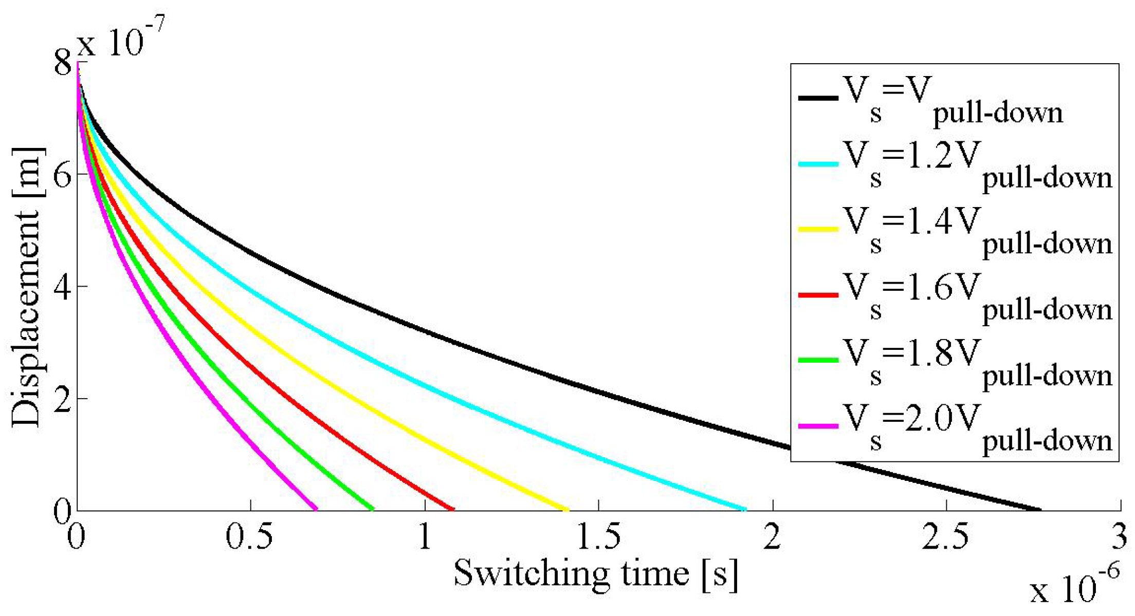
Figure 13 shows the dependence of the from different switching voltage () values.
Switching time analysis is critical to the design of RF MEMS switches, as achieving a short switching time from ON to OFF is a major challenge. It should be noted that the time of pull-down is slightly longer than the time of return to the initial state even in the case of a significantly greater potential difference than the .
Figure 14 and Figure 15 present graphs of the dependence of the total capacitance of the membrane taking into account the perforation in the down- and initial state on the thickness of the dielectric film deposited on the surface of the fixed down electrode.
Table 4 presents the calculated values of the coefficient of stiffness of elastic suspension elements, pull- and hold-down voltage, return voltage, switching time in the down and initial states.
3.4. Development and Modeling of Equivalent Circuit
For this integrated RF MEMS switch, the electrical impedance is determined by Equation (30):
For a given LC circuit the resonance frequency is determined by Equation (31):
Thus, the resistance of the switch can be represented by Equation (32):
The elastic fastening of the membrane plays an important role for the RF parameters of the switch, since they have inductance and resistance, affecting the passage of the RF signal.
To calculate the RF characteristics of the proposed design of an integrated RF MEMS switch LC isolation elements () for the control voltage from the RF signal were introduced into the existing electrical circuit which is implemented directly on the topology—capacitances located on the signal line () and membrane anchors () separating the constant control voltage from the RF signal. Inductance preventing the passage of the RF signal in power supply is located outside the circuit.
To calculate the inductance of the elastic fastening element () were used Equation (33) [76].
where —the length, width, thickness of the conductor.
When calculating the switch, the inductance resistance was calculated by Equation (34):
where —the resistivity of multilayer structure; L—the length of the conductor; S—the area of the conductor.
As a result of the calculations, the parameters of the electrical circuit of the proposed integrated RF MEMS switch were obtained, as shown in Table 5.
A electrical circuit of a integrated RF MEMS switch with LC isolation control signal is shown in Figure 16. The results of simulation of RF signal transmission are shown in Figure 17. Optimization and calculation of RF parameters of integrated RF MEMS switch is carried into effect in the Advanced Design System (ADS) CAD.
3.5. Technological Route of Manufacturing of the Developed Design of a RF MEMS Switch
The technological process of manufacturing an integrated RF MEMS switch is shown in Figure 18. The process is characterized by a low deposition temperature of layers (not more than 350 °C) in order to prevent damage to the CMOS IC.
At the beginning of the CMOS IC, it is manufactured using a standard CMOS process with formation of through holes. Then, the lower structural elements of the switch are formed, such as coplanar waveguide, fixed down electrode, anchor areas. The sacrificial layer is the photosensitive polyamide at various stages of formation of structural elements of the switch. Then, the upper structural elements such as the membrane, elastic suspension elements, the pair of side electrodes, the fixed upper electrode are formed. After forming the walls and cover for the capsule sealing, the sacrificial layers of polyamide are removed through holes in the capsule and fixed upper electrode membrane using dry etching. Finally, the holes in the capsule are sealed. The layer of sealing prevents switch failures that can be caused by contamination or high humidity. Consequently, the integrated RF MEMS switch shown in Figure 6 is manufactured using CMOS IC technology.
4. Conclusions
RF MEMS switches are of classic MEMS devices for RF and microwave applications. In these devices, mechanical motion is used to close or open the RF transmission line (for a given frequency band). In other words, the total input impedance of the RF transmission line is controlled by the mechanical motion of the moving element of the RF MEMS switch design.
The field of application of RF MEMS switches is rigidly connected with their parameters. Solid-state analogs of RF MEMS switches have a good combination of low-power consumption, high switching power, low insertion losses and high isolation value in the closed state. However, electromechanical parameters such as control voltage and switching time are characterized by extremely high values, which complicates their integration into RF control circuits and reduces the scope of application. Electromechanical parameters are interrelated and the improvement of some can lead to the deterioration of others. It is possible to distinguish several main directions of improvement of electromechanical parameters: replacement of traditionally used materials on new perspective, and development of new original designs and technological decisions.
The analytical approach to the development of RF MEMS switches allows us to develop designs with the best ratio of parameters for specific applications, which is demonstrated by the example of the developed design of an integrated RF MEMS switch with a capacitive switching principle with low control voltages, high switching speed and suitable for using in the X frequency range (8–12 GHz) in terrestrial and satellite radio communication devices.
Author Contributions
All authors contributed to the present paper with the same effort in finding available literature resources, as well as writing the paper.
Funding
This research received no external funding.
Acknowledgments
The results were obtained using Equipment of the student design bureau “Elements and devices of inertial navigation systems of robotics” of the Institute of Nanotechnologies, Electronics and Electronic Equipment Engineering, Southern Federal University (Taganrog, Russia).
Conflicts of Interest
The authors declare no conflict of interest.
References
- Rebeiz, G.M. RF MEMS: Theory, Design, and Technology; John Wiley & Sons: New York, NY, USA, 2004. [Google Scholar]
- Petersen, K.E. Micromechanical membrane switches on silicon. JBM J. Res. Dev. 1971, 23, 376–385. [Google Scholar] [CrossRef]
- Robin, L. Status of MEMS Industry; Tech. Rep.; Yole Developpement: Phoenix, AZ, USA, 2015; p. 7. [Google Scholar]
- Robin, L. Status of the MEMS Industry; Tech. Rep.; Yole Developpement: Phoenix, AZ, USA, 2017; p. 2. [Google Scholar]
- Hosaka, H.; Kuwano, H.; Yanagisawa, K. Electromagnetic microrelays: Concepts and fundamental characteristic. Sens. Actuators A 1994, 40, 41–47. [Google Scholar] [CrossRef]
- Taylor, W.P.; Allen, M.G.; Dauwalter, C.R. Batch fabricated electromagnetic microrelays. In Proceedings of the 45th Relay Conference, Lake Buena Vista, FL, USA, 23 July 1997; pp. 8.1–8.6. [Google Scholar]
- Taylor, W.P.; Allen, M.G. Integrated magnetic microrelays: Normally open, normally closed, and multi-pole devices. In Proceedings of the International Solid State Sensors and Actuators Conference (Transducers ’97), Chicago, IL, USA, 19 June 1997; pp. 1149–1152. [Google Scholar]
- Tilmans, H.A.; Fullin, E.; Ziad, H.; Van de Peer, M.D.; Kesters, J.; Van Geffen, E.; Bergqvist, J.; Pantus, M.; Beyne, E.; Baert, K.; et al. A fully-packaged electromagnetic microrelay. In Proceedings of the Technical Digest, IEEE International MEMS 99 Conference, Twelfth IEEE International Conference on Micro Electro Mechanical Systems, Orlando, FL, USA, 21 January 1999; pp. 25–30. [Google Scholar]
- Wright, J.A.; Tai, Y.-C. Magnetostatic MEMS relays for the miniaturization of brushless DC motor controllers. In Proceedings of the Technical Digest, Twelfth IEEE International Conference on Micro Electro Mechanical Systems, Orlando, FL, USA, 21 January 1999; pp. 594–599. [Google Scholar]
- Gretillat, M.A.; Gretillat, F.; Rooij, N.F. Micromechanical relay with electrostatic actuation and metallic contacts. J. Micromech. Microeng. 1999, 9, 324–331. [Google Scholar] [CrossRef]
- Sanders, C. MCNC Thermally Actuated Microrelays; News Release; MEMS Technology Application Center MCNC: Durham, NC, USA, 30 November 1998. [Google Scholar]
- Larson, L.E.; Hackett, R.H.; Lohr, R.F. Microactuators for GaAs-based microwave integrated circuits. In Proceedings of the 1991 International Conference on Solid-State Sensors and Actuators, Digest of Technical Papers, San Francisco, CA, USA, 24–27 June 1991; pp. 743–746. [Google Scholar]
- Yao, J.J.; Chang, M.F. A surface micromachined miniature switch for telecommunications applications with signal frequencies from DC up to 4 GHz. In Proceedings of the International Solid-State Sensors and Actuators Conference, Stockholm, Sweden, 25–29 June 1995; pp. 384–387. [Google Scholar]
- Schiele, I.; Huber, J.; Evers, C.; Hillerich, B.; Kozlowski, F. Micromechanical relay with electrostatic actuation. In Proceedings of the International Solid State Sensors and Actuators Conference, Chicago, IL, USA, 19 June 1997; pp. 1165–1168. [Google Scholar]
- De Los Santos, H.J.; Kao, Y.-H.; Caigoy, A.L.; Ditmars, E.D. Microwave and mechanical considerations in the design of MEM switches for aerospace applications. Proc. IEEE Aerosp. Conf. 1997, 3, 235–254. [Google Scholar]
- Hyman, D.; Lam, J.; Warneke, B.; Schmitz, A.; Hsu, T.Y.; Brown, J.; Schaffner, J.; Walston, A.; Loo, R.Y.; Mehregany, M.; et al. Surface-micromachined RF MEMS switches on GaAs substrates. Int. J. RF Microw. CAE 1999, 9, 348–361. [Google Scholar] [CrossRef]
- Hyman, D.; Schmitz, A.; Warneke, B.; Hsu, T.Y.; Lam, J.; Brown, J.; Schaffner, J.; Walston, A.; Loo, R.Y.; Tangonan, G.L.; et al. GaAs-compatible surface-micromachined RF MEMS switches. Electron. Lett. 1999, 35, 224–226. [Google Scholar] [CrossRef]
- Sovero, E.A.; Mihailovich, R.; Deakin, D.S.; Higgins, J.A.; Yao, J.J.; DeNatale, J.F.; Hong, J.H. Monolithic GaAs PHEMT MMICs integrated with high performance MEMS microrelays. In Proceedings of the 1999 SBMO/IEEE MTT-S International Microwave and Optoelectronics Conference, Rio de Janeiro, Brazil, 9–12 August 1999; pp. 257–260. [Google Scholar]
- Muldavin, J.B.; Rebeiz, G.M. 30 GHz tuned MEMS switches. In Proceedings of the 1999 IEEE MTT-S International Microwave Symposium Digest, Anaheim, CA, USA, 13–19 June 1999; pp. 1511–1514. [Google Scholar]
- Sakata, M.; Komura, Y.; Seki, T.; Kobayashi, K.; Sano, K.; Horiike, S. Micromachined relay which utilizes single crystal silicon electrostatic actuator. In Proceedings of the Technical Digest, IEEE International MEMS 99 Conference, Twelfth IEEE International Conference on Micro Electro Mechanical Systems, Orlando, FL, USA, 21 January 1999; pp. 21–24. [Google Scholar]
- Hiltmann, K.M.; Schmidt, B.; Sandmaier, H.; Lang, W. Development of micromachined switches with increased reliability. In Proceedings of the International Solid State Sensors and Actuators Conference, Chicago, IL, USA, 19 June 1997; pp. 1157–1160. [Google Scholar]
- Drake, J.; Jerman, H.; Lutze, B.; Stuber, M. An electrostatically actuated micro-relay. In Proceedings of the International Solid-State Sensors and Actuators Conference, Stockholm, Sweden, 25–29 June 1995; pp. 380–383. [Google Scholar]
- Admschik, M.; Ertl, S.; Schmid, P.; Gluche, P.; Floter, A.; Kohn, E. Electrostatic diamond micro switch. In Proceedings of the 10th International Conference on Solid-State Sensors and Actuators, Sendai, Japan, 7–10 June 1999; pp. 1284–1287. [Google Scholar]
- Gretillat, M.A.; Thiebaud, P.; Linder, C.; Rooij, N.F. Integrated circuit compatible polysilicon microrelays. J. Micromech. Microeng. 1995, 5, 156–160. [Google Scholar] [CrossRef]
- Simon, J.; Saffer, S.; Kim, C.-J. A micromechanical relay with a thermally-driven mercury micro-drop. In Proceedings of the Ninth International Workshop on Micro Electromechanical Systems, San Diego, CA, USA, 11–15 February 1996; pp. 515–520. [Google Scholar]
- Saffer, S.; Simon, J.; Kim, C.-J. Mercury-contact switching with gap-closing microcantilever. Proc. SPIE 1996, 2882, 204–208. [Google Scholar]
- Sun, X.-Q.; Farmer, K.R.; Carr, W.N. A bistable microrelay based on two-segment multimorph cantilever actuators. In Proceedings of the Eleventh Annual International Workshop on Micro Electro Mechanical Systems. An Investigation of Micro Structures, Sensors, Actuators, Machines and Systems, Heidelberg, Germany, 25–29 January 1998; pp. 154–159. [Google Scholar]
- Kruglick, E.J.J.; Pister, K.S.J. Bistable MEMS relays and contact characterization. In Proceedings of the Solid State Sensor and Actuator Workshop, Hilton Head Island, SC, USA, 8–11 June 1998; pp. 333–337. [Google Scholar]
- Robin, L. Status of MEMS Industry; Tech. Rep.; Yole Developpement: Phoenix, AZ, USA, 2013; pp. 7–8. [Google Scholar]
- Senturia, S.D. Microsystem Design, 1st ed.; Springer: New York, NY, USA, 2001. [Google Scholar]
- Mercier, D.; Caekenberghe, K.; Rebeiz, G.M. Miniature RF MEMS Switched Capacitors. In Proceedings of the IEEE MTT-S International Microwave Symposium Digest, Long Beach, CA, USA, 17 June 2005; pp. 745–748. [Google Scholar]
- Mercier, D.; Charvet, P.L.; Berruyer, P.; Zanchi, C.L.; Lapierre, L.O.; Vendier, O.; Cazaux, J.L.; Blondy, P. A DC to 100 GHz high performance ohmic shunt switch. In Proceedings of the 2004 IEEE MTT-S International Microwave Symposium Digest, Fort Worth, TX, USA, 6–11 June 2004; pp. 1931–1934. [Google Scholar]
- Lacroix, B.; Pothier, A.; Crunteanu, A.; Cibert, C.; Dumas-Bouchiat, F.; Champeaux, C.; Catherinot, A.; Blondy, P. Sub-microsecond RF MEMS switched capacitors. IEEE Trans. Microw. Theory Tech. 2007, 55, 1314–1321. [Google Scholar] [CrossRef]
- Majumder, S.; Lampen, J.; Morrison, R.; Maciel, J. A Packaged, High-Lifetime Ohmic MEMS RF Switch. IEEE MTT-S Int. Microw. Symp. Dig. 2003, 3, 1935–1938. [Google Scholar]
- Yan, X.; McGruer, N.E.; Adams, G.G.; Majumder, S. Thermal Characteristics of Microswitch Contacts. In Proceedings of the National Association of Relay Manufacturer’s (NARM) 49th Annual International Relay Conference, Oak Brook, IL, USA, 23–25 April 2001. [Google Scholar]
- Randy, J.; Richards; Hector, J.; De Santos, H.J. MEMS for RF/Microwave Wireless Applications: The Next Wave. Microw. J. 2001, 44, 20. [Google Scholar]
- Goldsmith, C.; Lin, T.-H.; Powers, B.; Wu, W.-R.; Norvell, B. Micromechanical membrane switches for microwave applications. In Proceedings of the 1995 IEEE MTT-S International Microwave Symposium, Orlando, FL, USA, 16–20 May 1995; pp. 91–94. [Google Scholar]
- Jaafar, H.; Sidek, O.; Miskam, A.; Korakkottil, S. Design and Simulation of Microelectromechanical System Capacitive Shunt Switches. Am. J. Eng. Appl. Sci. 2009, 2, 655–660. [Google Scholar]
- Ya, M.L.; Soin, N.; Nordin, A.N. Theoretical and simulated investigation of dielectric charging effect on a capacitive RF-MEMS switch. In Proceedings of the 2016 IEEE International Conference on Semiconductor Electronics (ICSE), Kuala Lumpur, Malaysia, 17–19 August 2016; pp. 17–20. [Google Scholar]
- San, H.S.; Deng, Z.Q.; Yu, Y.X.; Li, G.; Chen, X.Y. Study on dielectric charging in low-stress silicon nitride with the MIS structure for reliable MEMS applications. J. Micromech. Microeng. 2011, 21, 125019. [Google Scholar] [CrossRef]
- Zaghloul, U.; Coccetti, F.; Papaioannou, G.J.; Pons, P.; Plana, R. A novel low cost failure analysis technique for dielectric charging phenomenon in electrostatically actuated MEMS devices. In Proceedings of the 48th Annual IEEE International Reliability Physics Symposium (IRPS), Anaheim, CA, USA, 2–6 May 2010; pp. 237–245. [Google Scholar]
- Zaghloul, U.; Papaioannouc, G.; Coccettia, F.; Ponsa, P.; Planaa, R. Dielectric charging in silicon nitride films for MEMS capacitive switches: Effect of film thickness and deposition conditions. Microelectron. Reliab. 2009, 49, 1309–1314. [Google Scholar] [CrossRef]
- Li, M.; Zhao, J.; You, Z.; Zhao, G. Design and fabrication of a low insertion loss capacitive RF MEMS switch with novel micro-structures for actuation. Solid State Electron. 2016, 127, 32–37. [Google Scholar] [CrossRef]
- Chu, C.; Liao, X.; Yan, H. Ka-band RF MEMS capacitive switch with low loss, high isolation, long-term reliability and high-power handling based on GaAs MMIC technology. IET Microw. Antenna Propag. 2017, 11, 942–948. [Google Scholar] [CrossRef]
- Kwon, H.; Choi, D.J.; Park, J.H.; Lee, H.C. Contact materials and reliability for high-power RF-MEMS switches. In Proceedings of the International Conference on MICRO Electro Mechanical Systems, Hyogo, Japan, 21–25 January 2007; pp. 231–234. [Google Scholar]
- Coutu, R.A.; Kladitis, P.E.; Leedy, K.D.; Crane, R.L. Selecting metal alloy electric contact materials for MEMS switches. J. Micromech. Microeng. 2004, 14, 1157. [Google Scholar] [CrossRef]
- Coutu, R.A.; Reid, J.R.; Cortez, R.; Strawser, R.E.; Kladitis, P.E. Microswitches with sputtered Au, AuPd, Au-on-AuPt, and AuPtCu alloy electric contacts. IEEE Trans. Compon. Packag. Technol. 2006, 29, 341–349. [Google Scholar] [CrossRef]
- Broue, A.; Dhennin, J.; Courtade, F.; Dieppedale, C.; Pons, P.; Lafontan, X.; Plana, R. Characterization of Au/Au, Au/Ru and Ru/Ru ohmic contacts in MEMS switches improved by a novel methodology. J. Micro/Nanolithogr. MEMS MOEMS 2010, 9, 041102-1–041102-8. [Google Scholar]
- Czaplewski, D.A.; Nordquist, C.D.; Dyck, C.W.; Patrizi, G.A.; Kraus, G.M.; Cowan, W.D. Lifetime limitations of ohmic contacting RF MEMS switches with Au, Pt and Ir contact materials due to accumulation of ‘friction polymer’ on the contacts. J. Micromech. Microeng. 2012, 22, 105005. [Google Scholar] [CrossRef]
- Liu, B.; Lv, Z.; He, X.; Liu, M.; Hao, Y.; Li, Z. Improving performance of the metal-to-metal contact RF MEMS switch with a Pt-Au microspring contact design. J. Micromech. Microeng. 2011, 21, 065038. [Google Scholar] [CrossRef]
- Patel, C.D.; Rebeiz, G.M. RF MEMS metal-contact switches with mn-contact and restoring forces and low process sensitivity. IEEE Trans. Microw. Theory. Tech. 2011, 59, 1230–1237. [Google Scholar] [CrossRef]
- Patel, C.D.; Rebeiz, G.M. A high-reliability high-linearity high-power RF MEMS metal-contact switch for DC-40-GHz applications. IEEE Trans. Microw. Theory 2012, 60, 3096–3112. [Google Scholar] [CrossRef]
- Tang, M.; Agarwal, A.; Li, J.; Zhang, Q.X.; Win, P.; Huang, J.M.; Liu, A.Q. An approach of lateral RF MEMS switch for high performance. In Proceedings of the Symposium on Design, Test, Integration and Packaging of MEMS/MOEMS, Cannes, France, 7 May 2003. [Google Scholar]
- Puyal, V.; Dragomirescu, D.; Villeneuve, C.; Ruan, J.; Pons, P.; Plana, R. Frequency scalable model for MEMS capacitive shunt switches at millimeter-wave frequencies. IEEE Trans. Microw. Theory Tech. 2009, 57, 2824–2833. [Google Scholar] [CrossRef]
- Ekkels, P.; Rottenberg, X.; Puers, R.; Tilmans, H.A.C. Evaluation of platinum as a structural thin film material for RF-MEMS devices. J. Micromech. Microeng. 2009, 19, 065010–065018. [Google Scholar] [CrossRef]
- Palego, C.; Deng, J.; Peng, Z.; Halder, S.; Hwang, J.C.M.; Forehand, D.I.; Scarbrough, D.; Goldsmith, C.L.; Johnston, I.; Sampath, S.K.; et al. Robustness of RF MEMS capacitive switches with molybdenum membranes. IEEE Trans. Microw. Theory Tech. 2009, 57, 3262–3269. [Google Scholar] [CrossRef]
- Alam, A.H.M.Z.; Islam, M.R.; Khan, S.; Mohd Sahar, N.B.; Zamani, N.B. Effects of MEMS material on designing a multiband reconfigurable antenna. Iran. J. Electr. Comput. Eng. 2009, 8, 112–118. [Google Scholar]
- Parate, O.; Gupta, N. Material selection for electrostatic microactuators using Ashby approach. Mater. Des. 2011, 32, 1577–1581. [Google Scholar] [CrossRef]
- Kuwabara, K.; Norio, S.; Hiroki, M.; Junichi, K.; Toshikazu, K.; Katsuyuki, M.; Hiromu, I. RF-MEMS Switch Structure for Low-Voltage Actuation and High-Density Integration. In Proceedings of the Extended Abstracts of the 2007 International Conference on Solid State Devices and Materials, Ibaraki, Japan, 18–21 September 2007; pp. 90–91. [Google Scholar]
- Lei, L.M.; Shun-Meen, K.; Tien-Yu, T.L.; Lianjun, L. A Mechanical Approach to Overcome RF MEMS Switch Stiction Problem. In Proceedings of the 53rd Electronic Components and Technology Conference, New Orleans, LA, USA, 27–30 May 2003; pp. 377–384. [Google Scholar]
- Haixia, Z.; Yilong, H.; Zhiyong, X.; Dongmei, L.; Finch, N.; Marchetti, J.; Keating, D.; Narasimha, V. Design of A Novel Bulk Micro-machined RF MEMS Switch. Int. J. Nonlinear Sci. Numer. Simul. 2002, 3, 369–374. [Google Scholar]
- Jun, S.C.; Huang, X.M.H.; Manolidis, M.; Zorman, C.A.; Mehregany, M.; Hone, J. Electrothermal tuning of Al-SiC nanomechanical resonators. Nanotechnology 2006, 17, 1506–1511. [Google Scholar] [CrossRef]
- Al-Dahleh, R.; Mansour, R.R. High-capacitance-ratio warped-beam capacitive MEMS switch designs. J. Microelectromech. Syst. 2010, 19, 538–547. [Google Scholar] [CrossRef]
- Chang, C.; Chang, P. Innovative micromachined microwave switch with very low insertion loss. Sens. Actuators A Phys. 2010, 79, 71–75. [Google Scholar] [CrossRef]
- Bozler, C.; Drangmeister, R.; Duffy, S.; Gouker, M.; Knecht, J.; Kushner, L.; Parr, R.; Rabe, S.; Travis, L. MEMS microswitch arrays for recofigurable distributed microwave components. In Proceedings of the IEEE Antennas and Propagation Society International Symposium, Salt Lake City, UT, USA, 16–21 July 2000; pp. 587–591. [Google Scholar]
- Entesari, K.; Rebeiz, G.M. A differential 4-bit 6.5-10-GHz RFMEMS tunable filter. IEEE Trans. Microw. Theory Tech. 2005, 53, 1103–1110. [Google Scholar] [CrossRef]
- Demirel, K.; Yazgan, E.; Demir, S.; Akin, T. A new temperature-tolerant RF MEMS switch structure design and fabrication for Ka-Band applications. J. Microelectromech. Syst. 2016, 25, 60–68. [Google Scholar] [CrossRef]
- Fernandez-Bolanos, M.; Tsamados, D.; Dainesi, P.; Ionescu, A.M. Reliability of RF MEMS capacitive switches and distributed MEMS phase shifters using AlN dielectric. In Proceedings of the IEEE 22nd International Conference on Micro Electro Mechanical Systems, Sorrento, Italy, 25–29 January 2009; pp. 638–641. [Google Scholar]
- Roark, R.J.; Young, W.C. Formulas for Stress and Strain, 6th ed.; McGraw-Hill: New York, NY, USA, 1989. [Google Scholar]
- Yun, W. A Surface Micromachined Accelerometer with Integrated CMOS Detection Circuitry. Ph.D. Thesis, University of California at Berkeley, Berkeley, CA, USA, 1992. [Google Scholar]
- Fedder, G.K. Simulation of Microelectromechanical Systems. Ph.D. Thesis, University of California at Berkeley, Berkeley, CA, USA, 1994. [Google Scholar]
- Peroulis, D.; Pacheco, S.P.; Sarabandi, K.; Katehi, L.P.B. Electromechanical considerations in developing low-voltage RF MEMS switches. IEEE Trans. Microw. Theory Tech. 2003, 51, 259–270. [Google Scholar] [CrossRef]
- Shekhar, S.; Vinoy, K.J.; Ananthasuresh, G.K. Switching and Release Time Analysis of Electrostatically Actuated Capacitive RF MEMS Switches. Sens. Transducers J. 2011, 130, 77–90. [Google Scholar]
- Palmer, H.B. Capacitance of a parallel-plate capacitor by the Schwartz-Christoffel transformation. Trans. AIEE 1927, 56, 363. [Google Scholar]
- Koushik, G.; Mithlesh, K.; Saurabh, A.; Srimanta, B. A modified capacitance model of RF MEMS shunt switch incorporating fringing field effects of perforated beam. Solid-State Electron. 2015, 114, 35–42. [Google Scholar]
- Stojanovic, G.; Zivanovt, L.; Damjanovic, M. Compact Form of Expressions for Inductance Calculation of Meander Inductors. Serb. J. Electr. Eng. 2004, 1, 57–68. [Google Scholar] [CrossRef]
Figure 1.
Structure of the analytical approach.

Figure 2.
Schematic view of the resistive RF MEMS switch.

Figure 3.
Schematic view of the capacitive RF MEMS switch.

Figure 4.
Schematic view of sandwich structure.
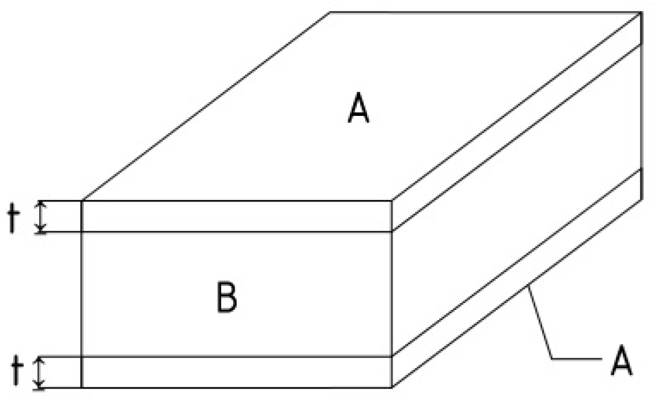
Figure 5.
Various support beams used to reduce the spring constant. (a) Fixed–fixed flexures. (b) Crab-leg flexures. (c) Folded flexures. (d) Serpentine flexures.
Figure 5.
Various support beams used to reduce the spring constant. (a) Fixed–fixed flexures. (b) Crab-leg flexures. (c) Folded flexures. (d) Serpentine flexures.
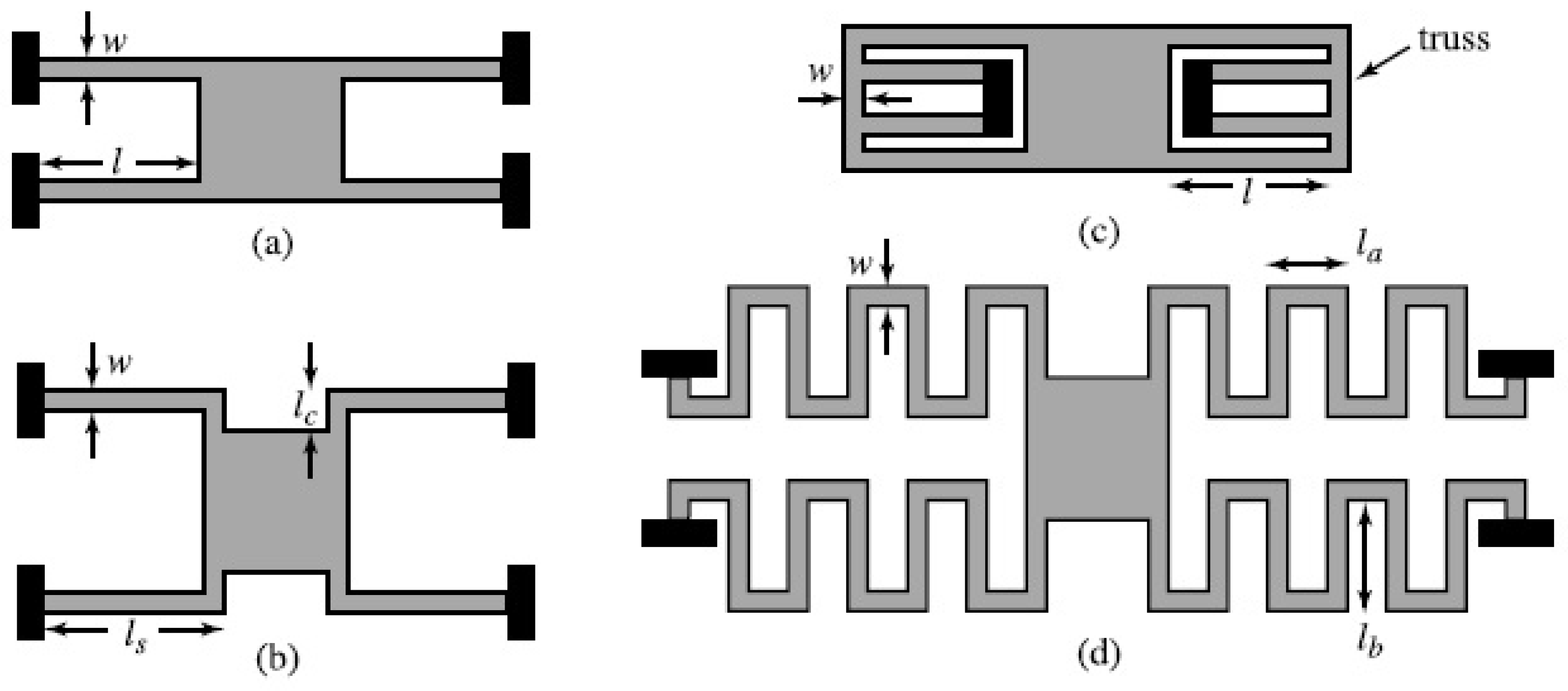
Figure 6.
Schematic view of the developed design of the integrated RF MEMS switch.

Figure 7.
View of the elastic suspension element.
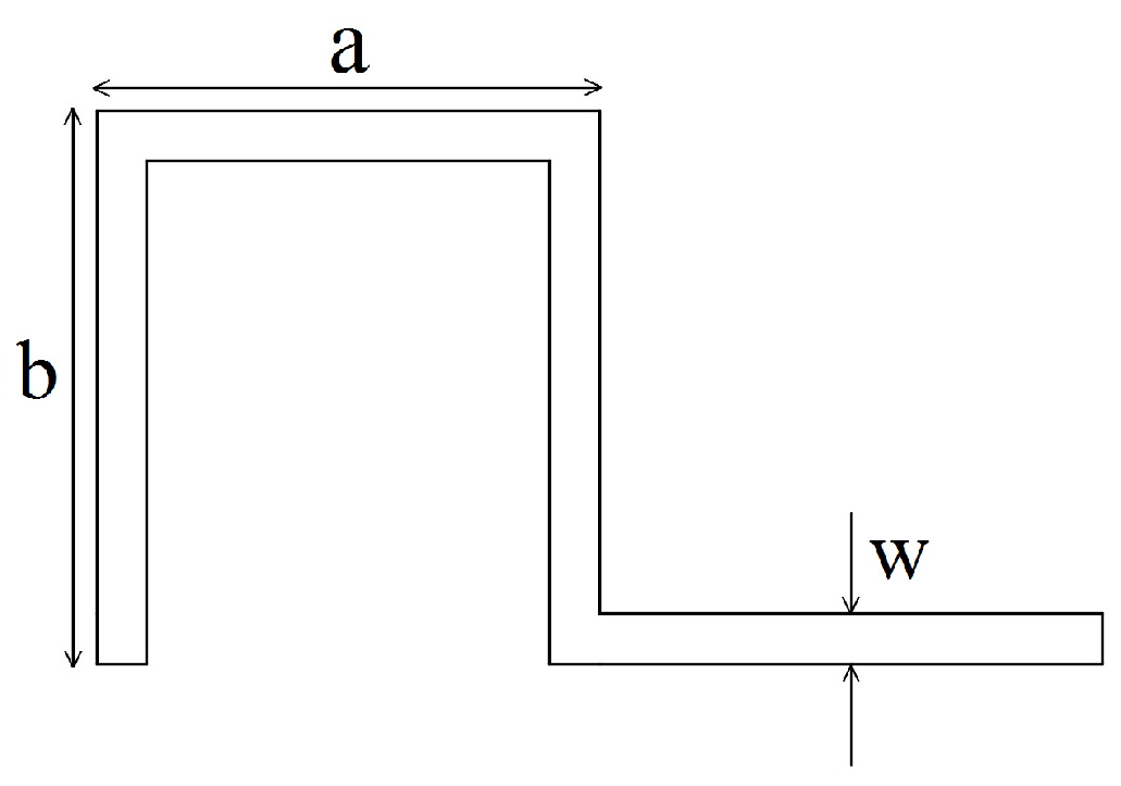
Figure 8.
One-dimensional model of the integrated RF MEMS switch.

Figure 9.
A parallel plate with thickness t.
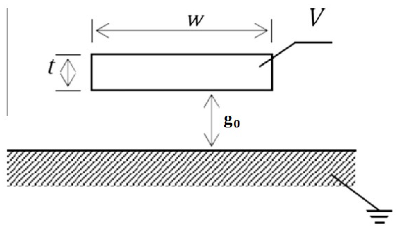
Figure 10.
Displacement of the membrane from the applied bias voltage.
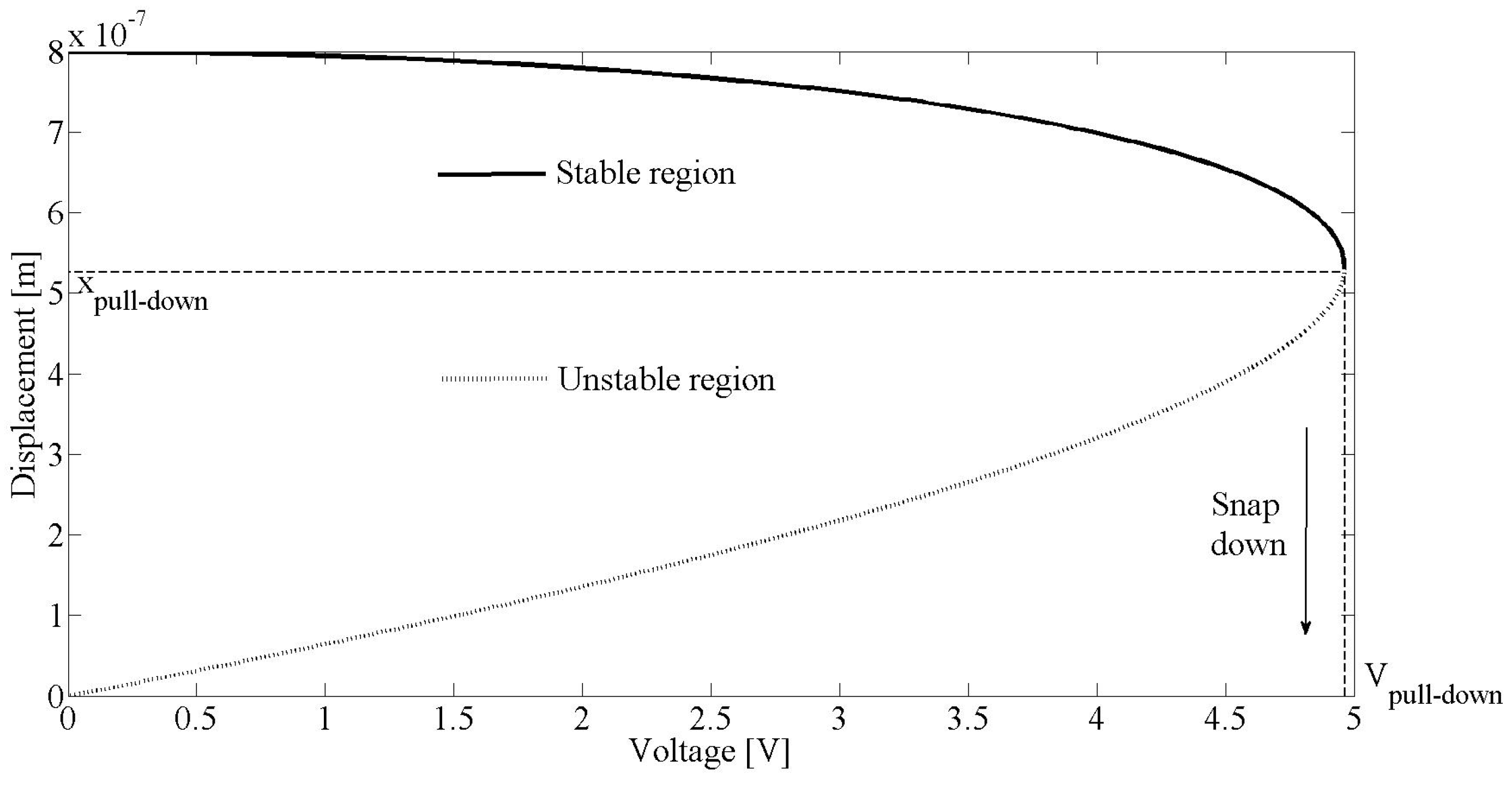
Figure 11.
Graph of dependence of the coefficient of elasticity on the number of meanders.
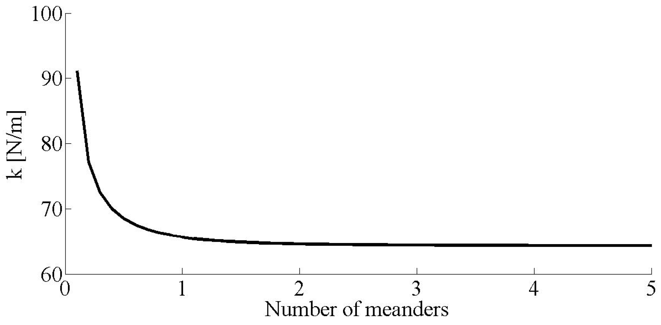
Figure 12.
The dependence of the pull-down voltage on the stiffness coefficient.
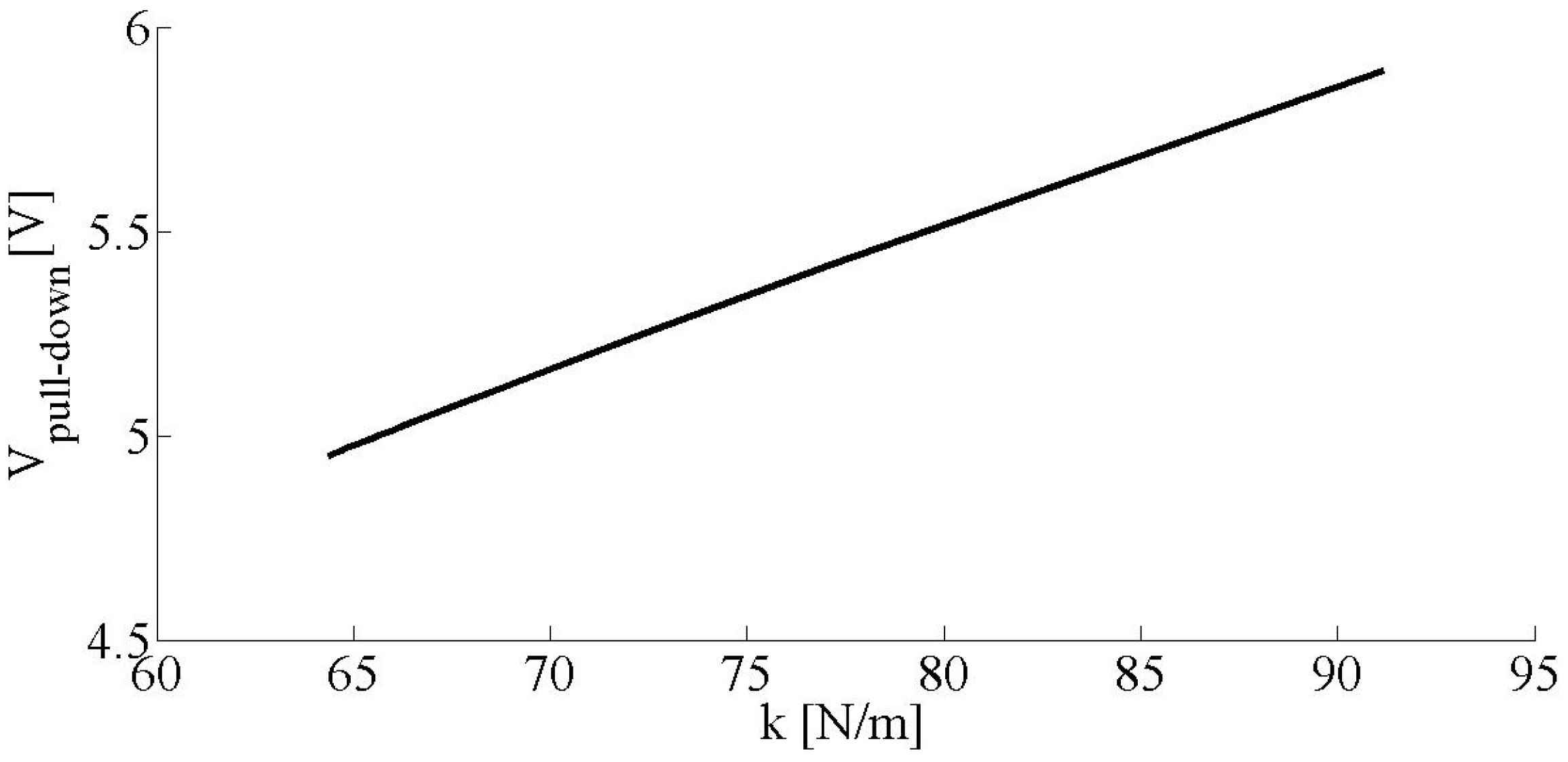
Figure 13.
The switching time simulation.

Figure 14.
Capacitance in the up-state.

Figure 15.
Capacitance in the down-state.
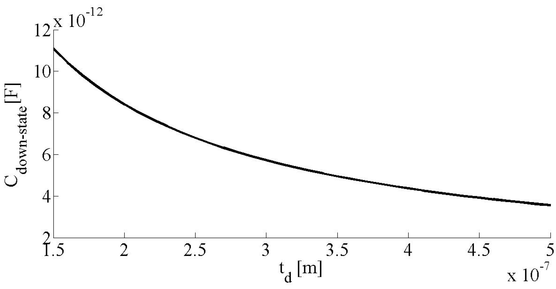
Figure 16.
The electrical circuit of the integrated RF MEMS switch with LC isolation control signal.
Figure 16.
The electrical circuit of the integrated RF MEMS switch with LC isolation control signal.

Figure 17.
Passing RF signal through the switch: (a) in down state; (b) in up state.
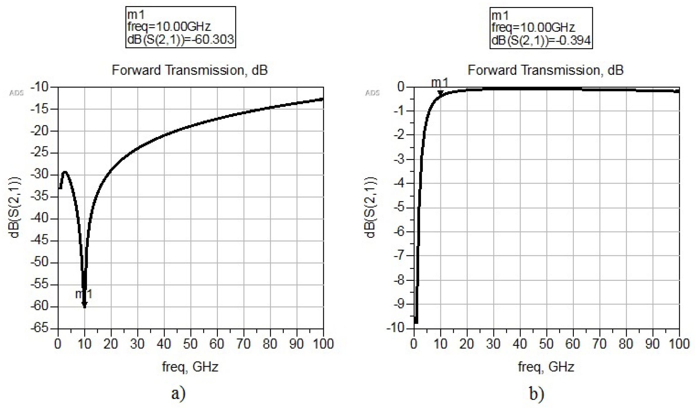
Figure 18.
Technological route of integrated RF MEMS switch manufacturing.


Table 1.
Materials of integrated RF MEMS switch.
| Structural Element | Material |
|---|---|
| Coplanar waveguide | Al |
| membrane | TiN/Al/TiN |
| Fixed down electrode | Al |
| Fixed upper electrode | TiN/Al/TiN |
| Second electrostatic drive | TiN/Al/TiN |
| Anchor area | Al |
| Dielectric layer | Si3N4 |
| Elastic suspension elements | TiN/Al/TiN |
| Substrate | SiO2-well in Si-substrate |
| SOI technology |
Table 2.
The topological dimensions of the structure elements of integrated RF MEMS switch.
| Structural Element | Dimension, µm |
|---|---|
| Signal line | 600 × 150 × 1 |
| Ground line | 600 × 100 × 1 |
| membrane | 300 × 300 × 2 |
| Hole in the membrane | 5 × 5 × 2 |
| Fixed down electrode | 400 × 150 × 1 |
| Fixed upper electrode | 400 × 300 × 2 |
| Elastic suspension elements | 50 × 2 × 2 |
| Dielectric film | 300 × 150 × 0.15 |
| Air gap | 0.8 |
| Anchor area | 50 × 10 × 0.8 |
| Substrate | 600 × 600 × 100 |
Table 3.
The material properties of the sandwich structure
| E, GPa | , 10−6 (°C−1) | K, W/m·K | , Ω·m | Density, kg·m3 | |
|---|---|---|---|---|---|
| 57.5 | 0.3175 | 16.7 | 196.55 | 6.32 × 10⁻⁸ | 4 × 10³ |
Table 4.
Calculated values of the coefficient of stiffness, pull- and hold-down voltage, return voltage, switching time.
Table 4.
Calculated values of the coefficient of stiffness, pull- and hold-down voltage, return voltage, switching time.
| N | k, N/m | Vpull-down, V | Vhold-down, V | Vreturn, V | Vpull-down, µs | Vpull-up, µs |
|---|---|---|---|---|---|---|
| 1 | 65.65 | 5 | 3.8 | 0.89 | 9.3 | 2.1 |
Table 5.
Calculated parameters of the electrical circuit.
| Parameter | Value |
|---|---|
| L | 0.0375 nH |
| R | 0.0341 Ω·m |
| 1.1 pF | |
| 22.12 pF | |
| 41.4 pF | |
| 0.011 pF |
© 2018 by the authors. Licensee MDPI, Basel, Switzerland. This article is an open access article distributed under the terms and conditions of the Creative Commons Attribution (CC BY) license (http://creativecommons.org/licenses/by/4.0/).
Share and Cite
MDPI and ACS Style
Lysenko, I.E.; Tkachenko, A.V.; Sherova, E.V.; Nikitin, A.V. Analytical Approach in the Development of RF MEMS Switches. Electronics 2018, 7, 415. https://doi.org/10.3390/electronics7120415
AMA Style
Lysenko IE, Tkachenko AV, Sherova EV, Nikitin AV. Analytical Approach in the Development of RF MEMS Switches. Electronics. 2018; 7(12):415. https://doi.org/10.3390/electronics7120415
Chicago/Turabian StyleLysenko, Igor E., Alexey V. Tkachenko, Elena V. Sherova, and Alexander V. Nikitin. 2018. "Analytical Approach in the Development of RF MEMS Switches" Electronics 7, no. 12: 415. https://doi.org/10.3390/electronics7120415
Note that from the first issue of 2016, this journal uses article numbers instead of page numbers. See further details here.