AlGaN/GaN MIS-HEMT with PECVD SiNx, SiON, SiO2 as Gate Dielectric and Passivation Layer


1
Engineering Research Center for Optoelectronics of Guangdong Province, School of Electronics and Information Engineering, South China University of Technology, Guangzhou 510640, China
2
School of Physics and Optoelectronics, South China university of Technology, Guangzhou 510640, China
3
Zhongshan Institute of Modern Industrial Technology, South China University of Technology, Zhongshan 528437, China
*
Author to whom correspondence should be addressed.
Electronics 2018, 7(12), 416; https://doi.org/10.3390/electronics7120416
Submission received: 5 October 2018
/
Revised: 6 December 2018
/
Accepted: 7 December 2018
/
Published: 10 December 2018
(This article belongs to the Special Issue Nanoelectronic Materials, Devices and Modeling)
Abstract
:Three different insulator layers SiNx, SiON, and SiO2 were used as a gate dielectric and passivation layer in AlGaN/GaN metal–insulator–semiconductor high-electron-mobility transistors (MIS-HEMT). The SiNx, SiON, and SiO2 were deposited by a plasma-enhanced chemical vapor deposition (PECVD) system. Great differences in the gate leakage current, breakdown voltage, interface traps, and current collapse were observed. The SiON MIS-HEMT exhibited the highest breakdown voltage and Ion/Ioff ratio. The SiNx MIS-HEMT performed well in current collapse but exhibited the highest gate leakage current density. The SiO2 MIS-HEMT possessed the lowest gate leakage current density but suffered from the early breakdown of the metal–insulator–semiconductor (MIS) diode. As for interface traps, the SiNx MIS-HEMT has the largest shallow trap density and the lowest deep trap density. The SiO2 MIS-HEMT has the largest deep trap density. The factors causing current collapse were confirmed by Photoluminescence (PL) spectra. Based on the direct current (DC) characteristics, SiNx and SiON both have advantages and disadvantages.
1. Introduction
In the past decades, the wide bandgap semiconductor material, gallium nitride (GaN), attracted great attention due to its wide bandgap, high breakdown electric field, and excellent thermal properties [1]. Gate leakage current and current collapse are the main issues that limit the performance of AlGaN/GaN high-electron-mobility transistors (HEMTs). To overcome these problems, different dielectric materials have been proposed for the fabrication of metal-insulator-semiconductor (MIS) HEMTs, such as SiO2 [2,3,4,5,6], SiNx [7,8,9,10,11], SiONe [12,13,14], ZrO2 [15], Al2O3 [16,17,18], and HfO2 [19], etc. Each material has advantages and disadvantages. Some groups studied stack dielectric layers like SiNx/Al2O3 [20] and SiNx/SiO2 [21] to improve leakage current and stability. The Al2O3 and HfO2 gate dielectric layer deposited by atomic layer deposition (ALD) has shown advantages in reducing gate leakage and eliminating current collapse [22,23]. However, Al2O3 and HfO2 are not suitable as passivation layers due to the low deposition rate of ALD. The plasma-enhanced chemical vapor deposition (PECVD) is one of the key sectors in conventional GaN-based light emitting diode (LED) production lines and complementary metal–oxide–semiconductor (CMOS) production lines. Thus, lots of work has been done on PECVD-deposited silicon nitride, silicon oxide, and silicon oxynitride. Compared to SiNx, SiO2 has a larger conduction band offset with GaN, which is related to leakage current. However, SiNx has a relatively higher dielectric constant (~7), which contributes to better gate control of two dimensional electron gas ( 2DEG). As a trade-off, SiON can be modulated to retain some advantages from both SiNx and SiO2 and has been proved to be a good candidate for a gate dielectric [12]. Considering the passivation effect, these dielectric layers can reduce the surface states, modulate the strain, and improve the reliability [24,25,26]. Although some comparisons have been made on the above materials [13,27,28], some published data are often controversial and the overall result is still not sufficiently clear. This shows that many questions are still unanswered and a better understanding of the passivation effect on the device performance is required.
In this work, we have made comprehensive comparisons between MIS-HEMTs with PECVD-deposited SiNx, SiON, and SiO2 as a gate dielectric and passivation layer. The differences in direct current (DC) static characteristics and current collapse were investigated. The interface traps were studied by Capacitance versus Voltage (C-V) measurements and a pulse mode drain current versus gate-to-source voltage (Id-Vgs) test. The Photoluminescence (PL) spectra test was also applied to confirm the passivation effectiveness.
2. Materials and Methods
The AlGaN/GaN epilayer used in this work is grown on Si (111) substrate using metal–organic chemical vapor deposition (MOCVD). The epitaxial structure consists of a 3.5 μm GaN buffer layer, a 300 nm GaN channel layer, a 1 nm AlN interlayer, a 22 nm Al0.23Ga0.77N barrier layer, and a 3 nm GaN cap layer. A 2DEG mobility of 1831 cm2/V·s and a sheet carrier concentration of 8.3 × 1012 cm−2 are measured by Hall effect measurement.
The device fabrication of MIS-HEMT started with the cleaning of the epitaxial wafer with a standard solvent. Then, devices were isolated using BCl3 and Cl2 etching in an Inductively Coupled Plasma (ICP) system. Prior to the deposition of ohmic metal, surface treatment was performed by immersing in HCL for 60 s. The Ti/Al/Ni/Au metal stack was then deposited by E-beam evaporation. Rapid temperature annealing at 850 °C for 1 min in a N2 environment was then performed to form ohmic contact. The contact resistance was 2.11 Ω∙mm and the specific contact resistance was 1.75 × 10⁻⁴ Ω cm2, as extracted by a circular transmission line model. After that, SiNx, SiON, and SiO2 dielectric layers with a thickness of 20 nm were deposited separately on the surfaces of different AlGaN/GaN samples using PECVD. Additionally, a Si dummy wafer and an AlGaN/GaN dummy wafer were loaded, together with the sample, in each deposition process. The dielectric/AlGaN/GaN samples were used for PL spectra measurement. The thickness and refractive index of deposited thin films were measured for the dummy wafer using an ellipsometer. The deposition properties of SiNx, SiON, and SiO2 are listed in Table 1.
The dielectric layers above drain and source electrodes were then removed by ICP. Finally, all samples were carried out using the same gate contact process. A Ni/Au (50/150 nm) gate metal was deposited by E-Beam evaporation. All samples have the same epitaxial structure and fabrication process, except for the type of dielectric layers. The MIS-HEMTs with different dielectric layers are labeled as SiNx MIS-HEMT, SiON MIS-HEMT, and SiO2 MIS-HEMT, respectively. Figure 1 shows the schematic cross-sectional view of MIS-HEMT. The gate length LG, gate width WG, gate to drain distance LGD, and gate to source distance LGS are 3, 150, 20, and 10 μm, respectively.
3. Results and Discussion
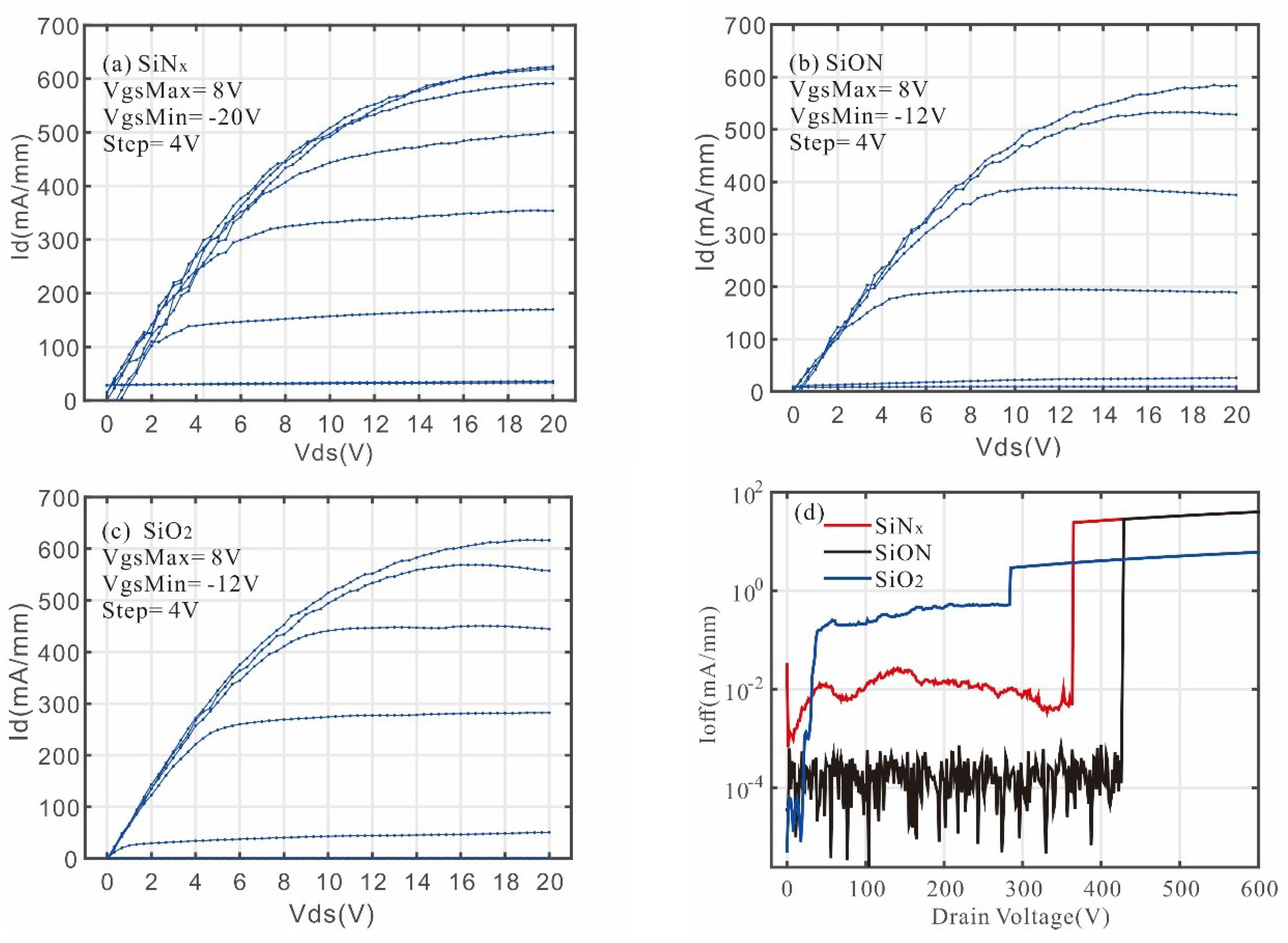
Table 2 shows some selected properties of MIS-HEMTs. The typical DC output characteristics of SiNx MIS-HEMT, SiON MIS-HEMT, and SiO2 MIS-HEMT are shown in Figure 2a–c. The drain current densities at drain-to-source voltage Vds = 20 V and gate-to-source voltage Vgs = 8 V are 623 mA/mm, 590 mA/mm, and 620 mA/mm, respectively, for SiNx MIS-HEMT, SiON MIS-HEMT, and SiO2 MIS-HEMT. The specific on-resistance extracted at Vds = 3 V is 9.89 Ω∙mm, 11.6 Ω∙mm, and 11.4 Ω∙mm, respectively. These output characteristics show that the SiNx MIS-HEMT has the highest maximum drain current and lowest static on-resistance. Figure 2d shows the off-state breakdown characteristics measured at Vgs = −18 V. SiON MIS-HEMT exhibits a higher breakdown voltage compared with the other two samples. SiNx performs slightly better in improving the saturated drain current of MIS-HEMT, and SiON can withstand a higher electric field strength.
Figure 3d plots the gate-to-source two-terminal leakage current curve when Vgs changes from 5 to −40 V with drain electrode dangling. The gate-to-source leakage current (Igs) density of SiNx MIS-HEMT is 4.46 × 10⁻⁴ mA/mm at Vgs = 20 V, which is 1 order larger than that of SiON or SiO2 MIS-HEMT. This can be attributed to the lower conduction band offset of SiNx from GaN [12]. As for SiO2 MIS-HEMT, there is a rapid increase of leakage current when the gate voltage bias is lower than −35 V. This phenomenon means that the SiO2 dielectric layers are more easily damaged than SiNx and SiON.
The transfer curves of the three samples are shown in Figure 3a–c. The drain voltage was fixed at 15 V, and the minimum gate voltage was −20 V, −14 V, and −12 V, respectively, for SiNx MIS-HEMT, SiON MIS-HEMT, and SiO2 MIS-HEMT. The drain current, Id, is almost equal to the gate current, Ig, in the off-state for all samples. This result reveals that the off-state drain leakage current is mainly from the gate electrode. As a result, the comparison of the off-state drain currents of these two samples agrees with the two-terminal gate leakage current. A high Ion/Ioff ratio > 107 was observed on SiON MIS-HEMT and SiO2 MIS-HEMT, which is two orders larger than SiNx MIS-HEMT.
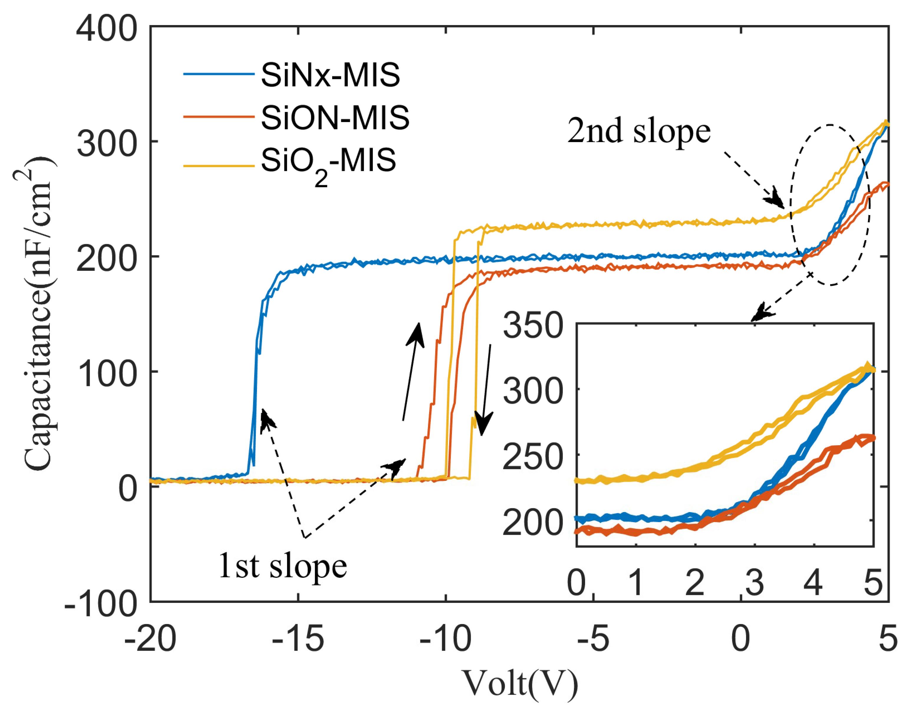
To investigate the interface condition of the three samples, a forward and backward C-V measurement with a frequency of 1 MHz was applied. As shown in Figure 4, each C-V curve has two rising slopes. The 1st slope represents the completed depletion of 2DEG and the 2nd slope indicates the electron transfer from AlGaN/GaN to dielectric/AlGaN interface [29,30]. A relatively low voltage corresponding to the 1st slope is observed in the SiNx MIS structure. This may be attributed to the fixed charge in the dielectric/AlGaN interface. Some researches show that a large amount of fixed charges exist in the dielectric layer and dielectric/AlGaN interface [31,32,33,34,35], differing from interface traps analyzed in the work, these kinds of fixed charges are not modulated by the gate voltage and do not lead to voltage hysteresis. Therefore, they have a negligible effect on the CV hysteresis measurement. However, the positive fixed charge would cause a negative voltage shift of the flat band voltage (VFB), and thus lead to a low threshold voltage, Vth [33]. More investigation concerning fixed charges is needed in the future. In the CV curve, the backward hysteresis and threshold voltage shifts are always attributed to interface traps. The inset of Figure 4 shows that there is little voltage shift on the 2nd slope while obvious hysteresis occurred on the 1st slope of the SiON and SiO2 MIS sample. This phenomenon occurs because larger number of deep traps with long emission time constants appear in the SiON and SiO2 MIS structure. We also used dielectric capacitance in series with the barrier capacitance model to extract the Cox of the three samples [36]. The Cox is 297.86, 277.82, and 364.82 nF/cm−2 for SiNx, SiON, and SiO2 MIS-HEMT, respectively. C-V measurement provides a rough comparison of the three structures but its precision is limited by the sweeping rates. The pulse-mode Id-Vgs measurement was employed for a more accurate extraction of interface states.
In this work, the pulse period was fixed at 500 ms and the selected measured pulse widths were 100 μs, 1 ms, 10 ms, 100 ms, and 200 ms. Vds was kept at 1 V to reduce drain-to-gate field-assisted detrapping [29]. The inset of Figure 5b shows the forward sweep and backward sweep measurement conditions of Vgs. It is reported that the acceptor-like interface states were originally empty and would capture electrons during the forward sweep of Vgs with a low Vgs base [29]; therefore, the forward sweep curve was chosen to be the basic line. In the backward sweep of Vgs, interface traps with emission times longer than the measurement pulse width would remain occupied by electrons, which would lead to a positive shift of Vth. The detectable traps emission time τ is related to its energy using Shockley-Read-Hall statistics:
where , , and are the electron thermal velocity, electron capture cross-section, and electron concentration at the effective density of states in the conduction band in GaN. ∆E = EC − ET is the energy gap between the conduction band and interface trap. k is the Boltzman constant and T is the temperature.
For SiNx MIS-HEMT, the forward Vgs base was −20 V. For SiON and SiO2 MIS-HEMT, the forward Vgs base was −14 V. The backward Vgs base was 5 V for all three samples. As shown in Figure 5a–c, SiNx MIS-HEMT shows a strong correlation between the measurement pulse width and the threshold voltage shift. SiO2 MIS-HEMT shows little Vth change with different pulse widths. The corresponding interface-trapped charge density (Qit) can be determined by:
where Cox values were extracted from C-V curves and the threshold voltage shift values were extracted from the results shown in Figure 5a–c.
Using Equations (1) and (2), Qit with different ranges of ∆E were extracted and are shown in Figure 5d. At ∆E > 0.460 eV, the Qit is , and for SiNx, SiON, and SiO2 MIS-HEMT, respectively. At ∆E > 0.657 eV, the Qit turns out to be , and respectively. SiN MIS-HEMT has the largest detected Qit at ∆E > 0.460 eV. These kinds of interface traps have an emission time longer than 100 μs. In the backward sweep of Vgs, these traps would remain occupied by an electron, and lead to the largest Vth shift observed in SiNx MIS-HEMT. In addition, the detectable Qit density of the SiNx sample includes a number of located at 0.460 eV < ∆E < 0.657 eV. These kind of traps (acceptor like) are regarded as shallow traps with short emission times. As for the SiO2 MIS-HEMT, the difference between Qit at ∆E > 0.460 eV and Qit at ∆E > 0.657 eV is small, which indicates that most of its interface traps are deep traps. In conclusion, SiNx MIS-HEMT has the largest density of shallow interface traps and the lowest density of deep traps among the three samples. SiO2 MIS-HEMT has the lowest density of shallow traps and largest density of deep traps. The performance of SiON MIS-HEMT is between the SiNx and SiO2 sample. These results explain the difference in hysteresis in the 1st slope of the C-V curve. The larger deep trap densities of SiON and SiO2 MIS-HEMT are responsible for the hysteresis in the 1st slope of the C-V curve. In addition, these calculated results show that shallow energy levels are more likely to be occupied by traps in the SiNx/AlGaN interface than in the SiON/AlGaN interface and SiO2/AlGaN interface. This offers chances for electron hopping, which could partially explain why SiNx MIS-HEMT has the highest gate leakage current and the lowest Ion/Ioff ratio among the three samples.
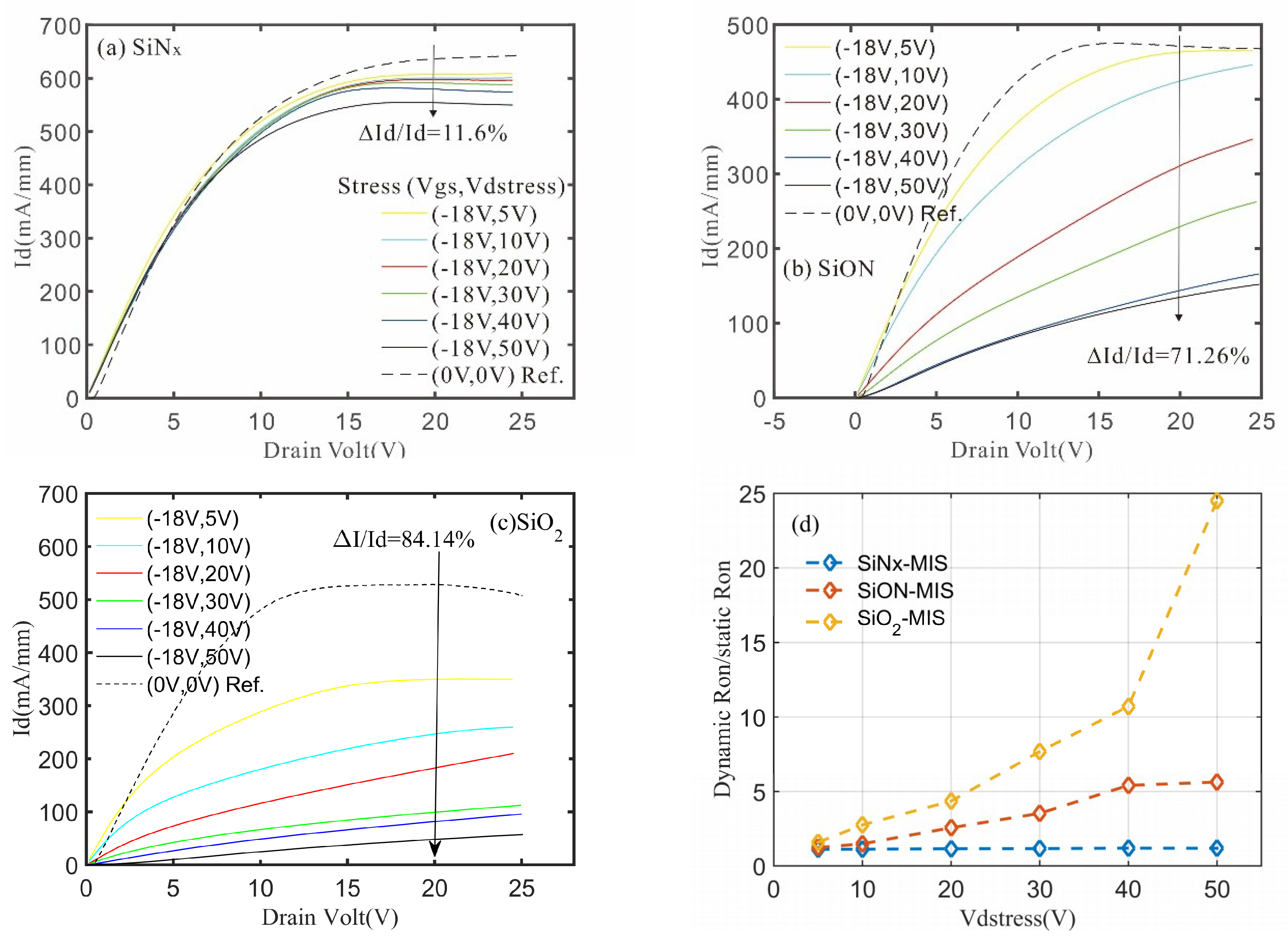
The Off-state Current collapse characteristic was measured by a slow switching test using an Agilent B1505A power device analyzer [37]. Various stress voltages from 5 V up to 50 V were applied on drain-to-source electrodes when Vgs was fixed at −18 V to ensure that the channel was pinched off. After the stress situation for 10 s, Vgs was changed to 0 V and the on-state Id-Vd curve was measured. In addition, the time interval was 10 ms between the two data points. This would lead to trap discharging and recover the current collapse to some extent. Therefore, the deep traps would be the major factor causing current collapse. Figure 6a–c shows that the degradation of the drain current was 11.6%, 71.26%, and 84.14%, respectively, for SiNx MIS-HEMT, SiON MIS-HEMT, and SiO2 MIS-HEMT. As Figure 6d shows, the dynamic Ron increases more quickly along with off-state drain bias stress (Vdstress) for SiO2 MIS-HEMT. After 50 V Vdstress was applied to the devices, the ratio of dynamic Ron and static Ron turns out to be 1.18, 5.64, and 24.5, respectively, for SiNx MIS-HEMT, SiON MIS-HEMT, and SiO2 MIS-HEMT. Among these three samples, SiNx MIS-HEMT shows better performance with regard to suppressing the current collapse than the other two samples. Though SiNx MIS-HEMT has the largest detected interface trap density, most of them are relatively shallow traps located at 0.46 eV < ∆E < 0.657 eV. These kinds of shallow traps contribute less to current collapse. SiON and SiO2 MIS-HEMT have higher trap density than SiNx MIS-HEMT at ∆E > 0.657 eV. This leads to more serious current collapse observed in SiON and SiO2 MIS-HEMT. The current collapse performance coincides with the extracted results of C-V and pulse Id-Vgs measurements for interface deep traps, which indicates that deep interface traps strongly influence the collapse characteristic.
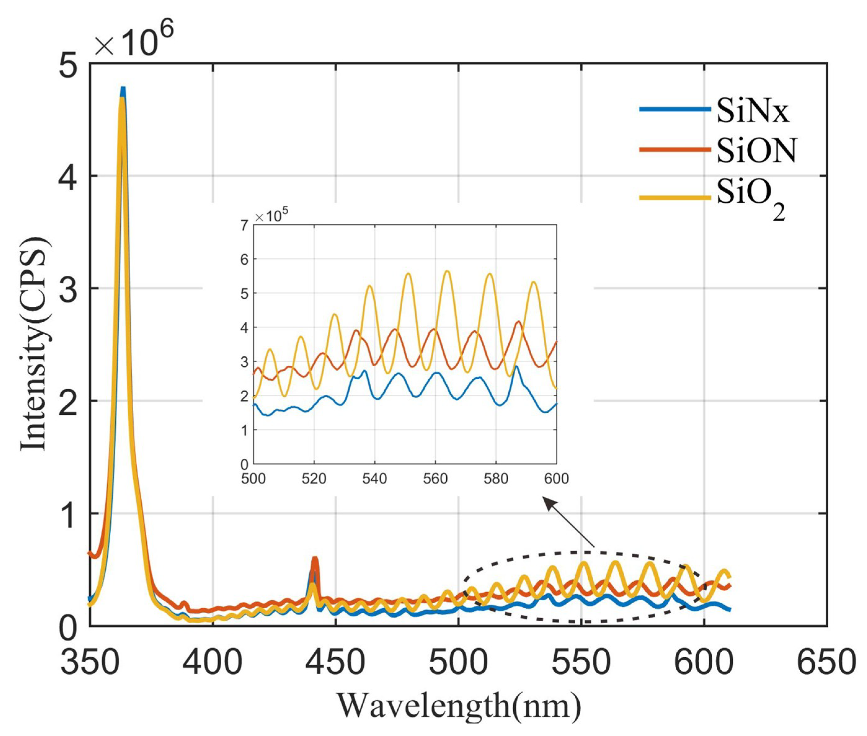
To further investigate the difference in characteristics of SiNx, SiON and SiO2 MIS-HEMT, room temperature photoluminescence (PL) spectra were recorded. As shown in the inset of Figure 7, the relative intensities of the yellow band (wavelength at approximately 560 nm) of the three dielectric/AlGaN/GaN samples are quite different. It has been reported that Si and O impurity, which would act as shallow donors, can effectively impact the yellow luminescence (YL) [38,39]. The largest YL intensity observed on SiO2/AlGaN/GaN sample implies that it has a maximum number of Si and O shallow donors among the three samples. During the deposition of SiON and SiO2, the reactive gas N2O would cause uncontrollable oxidation of the AlGaN interface and therefore generate several kinds of surface states [40]. The SiNx chemical deposition process involves NH3 plasma treatment, which would be effective to suppress the N-vacancies-related surface defects at the AlGaN surface [41]. When the off-state stress is applied to the devices, the shallow donors, oxides, and defects mentioned above would capture electrons and cause the phenomenon of the virtual gate [42]. The formation of the virtual gate would increase the depletion region and thus cause the decrease of drain current. The above factors together lead to the different performance on current collapse of the three samples.
4. Conclusions
In conclusion, we have fabricated AlGaN/GaN MIS-HEMTs with PECVD-deposited SiNx, SiON, and SiO2 as the gate dielectric and passivation layer. The DC static characteristics, interface traps, and current collapse of MIS-HEMTs with different dielectrics were comprehensively compared. The SiNx sample performs well with regard to suppressing the current collapse but suffers from high leakage current and high shallow trap density. The SiON MIS-HEMT exhibits a low gate leakage current of 3.86 × 10⁻⁵ mA/mm and a high breakdown voltage of 428 V, which indicates it is a great candidate as a gate dielectric and passivation layer. However, its deposition parameters need to be further optimized in order to enhance the reliability and stability.
Author Contributions
Conceptualization, K.G. and D.C.; Formal analysis, K.G. and D.C.; Investigation, Q.Z.; Methodology, K.G. and Q.Z.; Supervision, H.W.; Writing original draft, K.G. and D.C.; D.C. designed the experiment, prepared the samples and performed the measurements. K.G. contributed to the conception of the study and designed the experiment. Q.Z. contributed to the data analysis and wrote the manuscript. H.W. supervised the study and reviewed the manuscript.
Funding
This work was supported by Science and Technologies plan Projects of Guangdong Province (Nos. 2017B010112003, 2017A050506013), and Applied Technologies Research and Development Projects of Guangdong Province (Nos. 2015B010127013, 2016B010123004), and Science and Technologies plan Projects of Guangzhou City (Nos. 201504291502518, 201604046021, 201704030139), and Science and Technology Development Special Fund Projects of Zhongshan City (Nos. 2017F2FC0002, 2017A1009).
Conflicts of Interest
The authors declare no conflict of interest.
References
- Chen, K.J.; Haberlen, O.; Lidow, A.; Tsai, C.L.; Ueda, T.; Uemoto, Y.; Wu, Y. GaN-on-Si Power Technology: Devices and Applications. IEEE Trans. Electron. Dev. 2017, 64, 779–795. [Google Scholar] [CrossRef]
- Lee, J.; Kim, H.; Seo, K.; Cho, C.; Cha, H. High quality PECVD SiO2 process for recessed MOS-gate of AlGaN/GaN-on-Si metal–oxide–semiconductor heterostructure field-effect transistors. Solid State Electron. 2016, 122, 32–36. [Google Scholar] [CrossRef]
- Chakroun, A.; Jaouad, A.; Soltani, A.; Arenas, O.; Aimez, V.; Ares, R.; Maher, H. AlGaN/GaN MOS-HEMT Device Fabricated Using a High Quality PECVD Passivation Process. IEEE Electr. Device Lett. 2017, 38, 779–782. [Google Scholar] [CrossRef]
- Kordoš, P.; Heidelberger, G.; Bernát, J.; Fox, A.; Marso, M.; Lüth, H. High-power SiO2/AlGaN/GaN metal-oxide-semiconductor heterostructure field-effect transistors. Appl. Phys. Lett. 2005, 87, 143501. [Google Scholar] [CrossRef]
- Arulkumaran, S.; Egawa, T.; Ishikawa, H. Studies of Electron Beam Evaporated SiO2/AlGaN/GaN Metal—Oxide—Semiconductor High-Electron-Mobility Transistors. Jpn. J. Appl. Phys. 2005, 44. [Google Scholar] [CrossRef]
- Chiou, Y. Photo-CVD SiO2 Layers on AlGaN/GaN/AlGaN MOS-HFETs. J. Electrochem. Soc. 2004, 151, G863–G865. [Google Scholar] [CrossRef]
- Jiang, H.; Liu, C.; Chen, Y.; Lu, X.; Tang, C.W.; Lau, K.M. Investigation of Insitu SiN as Gate Dielectric and Surface Passivation for GaN MISHEMTs. IEEE Trans. Electron. Dev. 2017, 64, 832–839. [Google Scholar] [CrossRef]
- Tang, Z.; Jiang, Q.; Lu, Y.; Huang, S.; Yang, S.; Tang, X.; Chen, K.J. 600-V Normally Off SiNx/AlGaN/GaN MIS-HEMT With Large Gate Swing and Low Current Collapse. IEEE Electr Device Lett. 2013, 34, 1373–1375. [Google Scholar] [CrossRef]
- Zhang, Z.; Yu, G.; Zhang, X.; Deng, X.; Li, S.; Fan, Y.; Sun, S.; Song, L.; Tan, S.; Wu, D.; et al. Studies on High-Voltage GaN-on-Si MIS-HEMTs Using LPCVD Si3N4 as Gate Dielectric and Passivation Layer. IEEE Trans. Electron. Dev. 2016, 63, 731–738. [Google Scholar] [CrossRef]
- Arulkumaran, S.; Hong, L.Z.; Ing, N.G.; Selvaraj, S.L.; Egawa, T. Influence of Ammonia in the Deposition Process of SiN on the Performance of SiN/AlGaN/GaN Metal–Insulator–Semiconductor High-Electron-Mobility Transistors on 4-in. Si(111). Appl. Phys. Express 2009, 2, 31001. [Google Scholar] [CrossRef]
- Adivarahan, V.; Gaevski, M.; Sun, W.H.; Fatima, H.; Koudymov, A.; Saygi, S.; Simin, G.; Yang, J.; Khan, M.A.; Tarakji, A.; et al. Submicron gate Si3N4/AlGaN/GaN-metal-insulator-semiconductor heterostructure field-effect transistors. IEEE Electr. Device Lett. 2003, 24, 541–543. [Google Scholar] [CrossRef]
- Kim, H.; Han, S.; Jang, W.; Cho, C.; Seo, K.; Oh, J.; Cha, H. Normally-Off GaN-on-Si MISFET Using PECVD SiON Gate Dielectric. IEEE Electr. Device Lett. 2017, 38, 1090–1093. [Google Scholar] [CrossRef]
- Balachander, K.; Arulkumaran, S.; Egawa, T.; Sano, Y.; Baskar, K. A comparison on the Electrical Characteristics of SiO2, SiON and SiN as the Gate Insulators for the Fabrication of AlGaN/GaN Metal–Oxide/Insulator–Semiconductor High-Electron Mobility-Transistors. Jpn. J. Appl. Phys. 2005, 44, 4911–4913. [Google Scholar] [CrossRef]
- Balachander, K.; Arulkumaran, S.; Egawa, T.; Sano, Y.; Baskar, K. Demonstration of AlGaN/GaN metal-oxide-semiconductor high-electron-mobility transistors with silicon-oxy-nitride as the gate insulator. Mater. Sci. Eng. B 2005, 119, 36–40. [Google Scholar] [CrossRef]
- Balachander, K.; Arulkumaran, S.; Ishikawa, H.; Baskar, K.; Egawa, T. Studies on electron beam evaporated ZrO2/AlGaN/GaN metal-oxide-semiconductor high-electron-mobility transistors. Phys. Status Solidi A 2005, 202, R16–R18. [Google Scholar] [CrossRef]
- Ye, P.D.; Yang, B.; Ng, K.K.; Bude, J.; Wilk, G.D.; Halder, S.; Hwang, J.C.M. GaN metal-oxide-semiconductor high-electron-mobility-transistor with atomic layer deposited Al2O3 as gate dielectric. Appl. Phys. Lett. 2005, 86, 63501. [Google Scholar] [CrossRef]
- Liu, Z.H.; Ng, G.I.; Arulkumaran, S.; Maung, Y.K.T.; Teo, K.L.; Foo, S.C.; Sahmuganathan, V.; Xu, T.; Lee, C.H. High Microwave-Noise Performance of AlGaN/GaN MISHEMTs on Silicon with Al2O3 Gate Insulator Grown by ALD. IEEE Electr. Device Lett. 2010, 31, 96–98. [Google Scholar]
- Asif, M.; Chen, C.; Peng, D.; Xi, W.; Zhi, J. Improved DC and RF performance of InAlAs/InGaAs InP based HEMTs using ultra-thin 15 nm ALD-Al2O3 surface passivation. Solid State Electron. 2018, 142, 36–40. [Google Scholar] [CrossRef]
- Liu, C.; Chor, E.F.; Tan, L.S. Investigations of HfO2/AlGaN/GaN metal-oxide-semiconductor high electron mobility transistors. Appl. Phys. Lett. 2006, 88, 173504. [Google Scholar] [CrossRef]
- Anand, M.J.; Ng, G.I.; Vicknesh, S.; Arulkumaran, S.; Ranjan, K. Reduction of current collapse in AlGaN/GaN MISHEMT with bilayer SiN/Al2O3 dielectric gate stack. Phys. Status Solidi C 2013, 10, 1421–1425. [Google Scholar] [CrossRef]
- Balachander, K.; Arulkumaran, S.; Sano, Y.; Egawa, T.; Baskar, K. Fabrication of AlGaN/GaN double-insulator metal-oxide-semiconductor high-electron-mobility transistors using SiO2 and SiN as gate insulators. Phys. Status Solidi A 2005, 202, R32–R34. [Google Scholar] [CrossRef]
- Miyazaki, E.; Goda, Y.; Kishimoto, S.; Mizutani, T. Comparative study of AlGaN/GaN metal-oxide-semiconductor heterostructure field-effect transistors with Al2O3 and HfO2 gate oxide. Solid State Electron. 2011, 62, 152–155. [Google Scholar] [CrossRef]
- Chang, Y.C.; Huang, M.L.; Chang, Y.H.; Lee, Y.J.; Chiu, H.C.; Kwo, J.; Hong, M. Atomic-layer-deposited Al2O3 and HfO2 on GaN: A comparative study on interfaces and electrical characteristics. Microelectron. Eng. 2011, 88, 1207–1210. [Google Scholar] [CrossRef]
- Green, B.M.; Chu, K.K.; Chumbes, E.M.; Smart, J.A.; Shealy, J.R.; Eastman, L.F. The effect of surface passivation on the microwave characteristics of undoped AlGaN/GaN HEMTs. IEEE Electr. Device Lett. 2000, 21, 268–270. [Google Scholar] [CrossRef]
- Meneghesso, G.; Verzellesi, G.; Danesin, F.; Rampazzo, F.; Zanon, F.; Tazzoli, A.; Meneghini, M.; Zanoni, E. Reliability of GaN High-Electron-Mobility Transistors: State of the Art and Perspectives. IEEE Trans. Device Mater. Reliab. 2008, 8, 332–343. [Google Scholar] [CrossRef]
- Arulkumaran, S.; Ng, G.I.; Liu, Z.H. Effect of gate-source and gate-drain Si3N4 passivation on current collapse in AlGaN/GaN high-electron-mobility transistors on silicon. Appl. Phys. Lett. 2007, 90, 173504. [Google Scholar] [CrossRef]
- Arulkumaran, S.; Egawa, T.; Ishikawa, H.; Jimbo, T.; Sano, Y. Surface passivation effects on AlGaN/GaN high-electron-mobility transistors with SiO2, Si3N4, and silicon oxynitride. Appl. Phys. Lett. 2004, 84, 613–615. [Google Scholar] [CrossRef]
- Javorka, P.; Bernat, J.; Fox, A.; Marso, M.; Lüth, H.; Kordoš, P. Influence of SiO2 and Si3N4 passivation on AIGaN/GaN/Si HEMT performance. Electron. Lett. 2003, 39, 1155–1157. [Google Scholar] [CrossRef]
- Lu, X.; Yu, K.; Jiang, H.; Zhang, A.; Lau, K.M. Study of Interface Traps in AlGaN/GaN MISHEMTs Using LPCVD SiNx as Gate Dielectric. IEEE Trans. Electron. Dev. 2017, 64, 824–831. [Google Scholar] [CrossRef]
- Mizue, C.; Hori, Y.; Miczek, M.; Hashizume, T. Capacitance-Voltage Characteristics of Al2O3/AlGaN/GaN Structures and State Density Distribution at Al2O3/AlGaN Interface. Jpn. J. Appl. Phys. 2011, 50. [Google Scholar] [CrossRef]
- Capriotti, M.; Alexewicz, A.; Fleury, C.; Gavagnin, M.; Bethge, O.; Visalli, D.; Derluyn, J.; Wanzenböck, H.D.; Bertagnolli, E.; Pogany, D.; et al. Fixed interface charges between AlGaN barrier and gate stack composed of insitu grown SiN and Al2O3 in AlGaN/GaN high electron mobility transistors with normally off capability. Appl. Phys. Lett. 2014, 104, 113502. [Google Scholar] [CrossRef]
- Hung, T.; Krishnamoorthy, S.; Esposto, M.; Neelim Nath, D.; Sung Park, P.; Rajan, S. Interface charge engineering at atomic layer deposited dielectric/III-nitride interfaces. Appl. Phys. Lett. 2013, 102, 72105. [Google Scholar] [CrossRef]
- Zhu, J.; Ma, X.; Xie, Y.; Hou, B.; Chen, W.; Zhang, J.; Hao, Y. Improved Interface and Transport Properties of AlGaN/GaN MIS-HEMTs with PEALD-Grown AlN Gate Dielectric. IEEE Trans. Electron. Dev. 2015, 62, 512–518. [Google Scholar]
- Son, J.; Chobpattana, V.; McSkimming, B.M.; Stemmer, S. Fixed charge in high-k/GaN metal-oxide-semiconductor capacitor structures. Appl. Phys. Lett. 2012, 101, 102905. [Google Scholar] [CrossRef] [Green Version]
- Liu, S.; Huang, C.; Chang, C.; Lin, Y.; Chen, B.; Tsai, S.; Majlis, B.Y.; Dee, C.; Chang, E.Y. Effective Passivation with High-Density Positive Fixed Charges for GaN MIS-HEMTs. IEEE J. Electron. Dev. 2017, 5, 170–174. [Google Scholar] [CrossRef]
- Yang, S.; Liu, S.; Lu, Y.; Liu, C.; Chen, K.J. AC-Capacitance Techniques for Interface Trap Analysis in GaN-Based Buried-Channel MIS-HEMTs. IEEE Trans. Electron Dev. 2015, 62, 1870–1878. [Google Scholar] [CrossRef]
- Zhang, D.; Cheng, X.; Zheng, L.; Shen, L.; Wang, Q.; Gu, Z.; Qian, R.; Wu, D.; Zhou, W.; Cao, D.; et al. Effects of polycrystalline AlN film on the dynamic performance of AlGaN/GaN high electron mobility transistors. Mater. Des. 2018, 148, 1–7. [Google Scholar] [CrossRef]
- Reshchikov, M.A.; Morkoç, H. Luminescence properties of defects in GaN. J. Appl. Phys. 2005, 97, 61301. [Google Scholar] [CrossRef]
- Kaufmann, U.; Kunzer, M.; Obloh, H.; Maier, M.; Manz, C. Origin of defect-related photoluminescence bands in doped and nominally undoped GaN. Phys. Rev. B Condens. Matter 1999, 59, 5561. [Google Scholar] [CrossRef]
- Chevtchenko, S.A.; Reshchikov, M.A.; Fan, Q.; Ni, X.; Moon, Y.T.; Baski, A.A.; Morkoç, H. Study of SiNx and SiO2 passivation of GaN surfaces. J. Appl. Phys. 2007, 101, 1139–1190. [Google Scholar] [CrossRef]
- Hashizume, T.; Hasegawa, H. Effects of nitrogen deficiency on electronic properties of AlGaN surfaces subjected to thermal and plasma processes. Appl. Surf. Sci. 2004, 234, 387–394. [Google Scholar] [CrossRef] [Green Version]
- Eller, B.S.; Yang, J.; Nemanich, R.J. Electronic surface and dielectric interface states on GaN and AlGaN. J. Vacuum Sci. Technol. A Vacuum Surf. Films 2013, 31, 50807. [Google Scholar] [CrossRef]
Figure 1.
Metal–insulator–semiconductor high-electron-mobility transistors (MIS-HEMT) structure cross-section view.
Figure 1.
Metal–insulator–semiconductor high-electron-mobility transistors (MIS-HEMT) structure cross-section view.
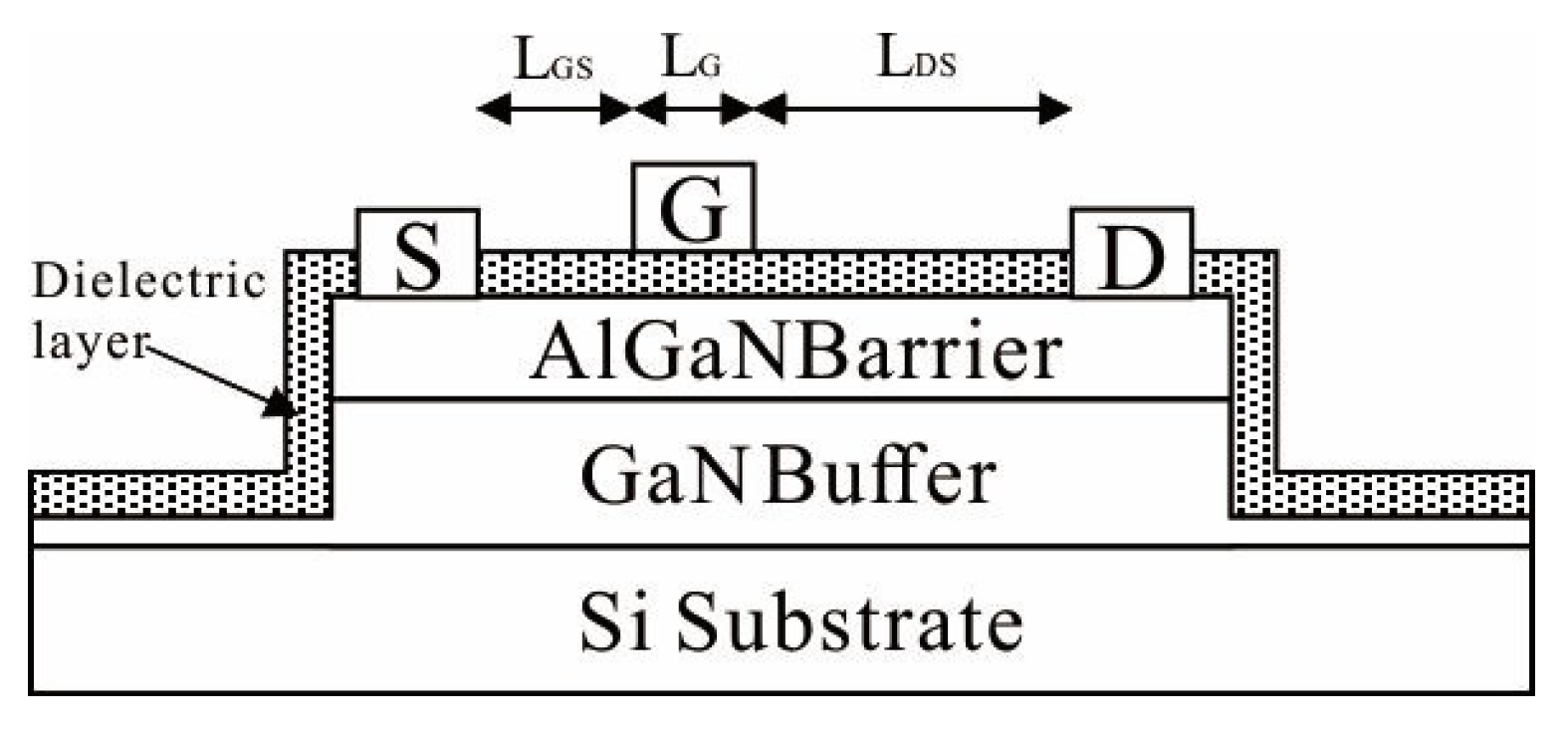
Figure 2.
Output characteristic of (a) SiNx MIS-HEMT, (b)SiON MIS-HEMT, and (c) SiO2 MIS-HEMT. (d) off-state breakdown characteristic of the three samples, measured at Vgs = −18 V.
Figure 2.
Output characteristic of (a) SiNx MIS-HEMT, (b)SiON MIS-HEMT, and (c) SiO2 MIS-HEMT. (d) off-state breakdown characteristic of the three samples, measured at Vgs = −18 V.

Figure 3.
Transfer characteristic of (a) SiNx MIS-HEMT, (b) SiON MIS-HEMT, and (c) SiO2 MIS-HEMT, and (d) gate leakage current curve measured at two terminals for the three samples.
Figure 3.
Transfer characteristic of (a) SiNx MIS-HEMT, (b) SiON MIS-HEMT, and (c) SiO2 MIS-HEMT, and (d) gate leakage current curve measured at two terminals for the three samples.
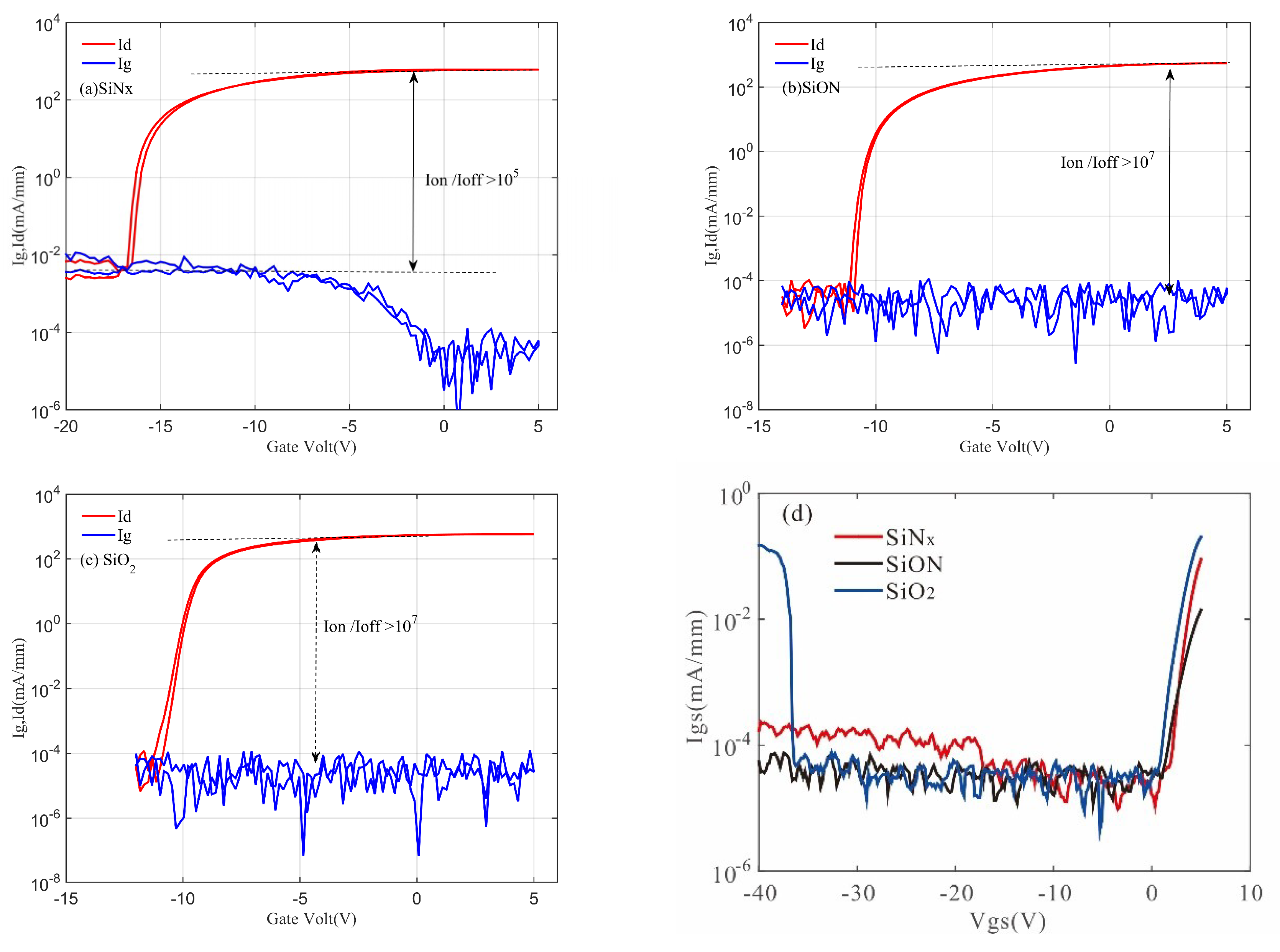
Figure 4.
Forward and backward capacitance versus voltage (C-V) measurement with frequency of 1 MHz. Inset: magnified voltage range of 0~5 V.
Figure 4.
Forward and backward capacitance versus voltage (C-V) measurement with frequency of 1 MHz. Inset: magnified voltage range of 0~5 V.

Figure 5.
Pulse mode Id-Vgs curves with pulse width variations of 100 μs, 1 ms, 10 ms, 100 ms, and 200 ms. The pulse period is 500 ms. The Vds was kept at 1 VThe backward Vgs base is 5 V. (a) SiNx MIS-HEMT with forward Vgs base of −20 V (b) SiON MIS-HEMT with forward Vgs base of −14 V. Inset: pulse Vgs condition with forward sweep and backward sweep (c) SiO2 MIS-HEMT with forward Vgs base of −14 V (d) Interface trap charge density Qit at ∆E > x(eV) of three samples.
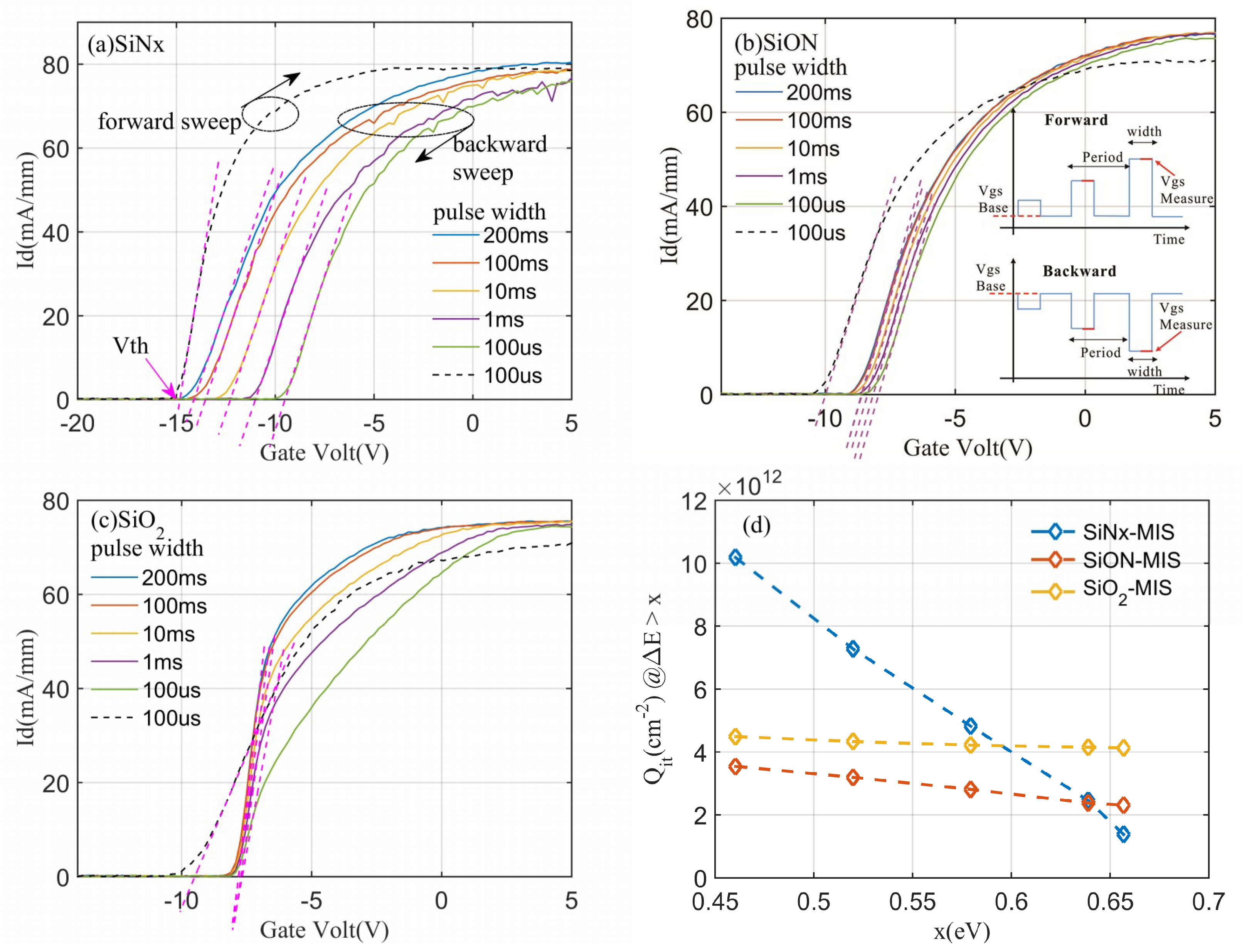
Figure 6.
Id-Vds curves at Vgs = 0 V of (a) SiNx MIS-HEMT (b) SiON MIS-HEMT (c) SiO2 MIS-HEMT after off-state stress bias at Vgs = −18 V, Vds stress at 5, 10, 20, 30, 40, and 50 V for 10 s. (d) The ratio of dynamic Ron and static Ron versus different off-state Vds stress.
Figure 6.
Id-Vds curves at Vgs = 0 V of (a) SiNx MIS-HEMT (b) SiON MIS-HEMT (c) SiO2 MIS-HEMT after off-state stress bias at Vgs = −18 V, Vds stress at 5, 10, 20, 30, 40, and 50 V for 10 s. (d) The ratio of dynamic Ron and static Ron versus different off-state Vds stress.

Figure 7.
Photoluminescence (PL) spectra at room temperature of three samples.


Table 1.
Deposition properties of SiNx, SiON, and SiO2.
| Sample | Pressure (millitorr) | RF Power(W) | SiH4 1 (sccm2) | N2O (sccm) | NH3 (sccm) | TEM (°C) | Refractive Index 3 |
|---|---|---|---|---|---|---|---|
| SiNx | 650 | 50 | 150 | 0 | 25 | 300 | 1.82 |
| SiON | 500 | 75 | 25 | 20 | 40 | 300 | 1.56 |
| SiO2 | 650 | 50 | 100 | 1000 | 0 | 300 | 1.46 |
1 SiH4 (5%)/N2; 2 Standard Cubic Centimeter per Minute; 3 Refractive Index at the wavelength of 632.8 nm.
Table 2.
Selected properties of SiNx, SiON, and SiO2 MIS-HEMT.
| Sample | Idmax (mA/mm) | gmmax (mS/mm) | Vth | Gate Leakage 1 (mA/mm) | Off-State Breakdown Voltage (V) | %I 2 | Dynamic Ron/Static Ron 3 |
|---|---|---|---|---|---|---|---|
| SiNx | 623 | 62.7 | −16.7 | 4.46 E-4 | 364 | 11.6% | 1.18 |
| SiON | 590 | 55.3 | −11.7 | 3.86 E-5 | 428 | 71.26% | 5.64 |
| SiO2 | 620 | 81.3 | −9.9 | 3.12 E-5 | 284 | 84.14% | 24.5 |
1 Gate leakage current density at two-terminal reverse voltage = −20 V; 2 Reduction of drain current and increase of Ron due to current collapse at off-state Vgs = −18 V, Vdstress = 50 V for 10 s; 3 Dynamic Ron at off-state Vds stress = 50 V and static Ron without stress.
© 2018 by the authors. Licensee MDPI, Basel, Switzerland. This article is an open access article distributed under the terms and conditions of the Creative Commons Attribution (CC BY) license (http://creativecommons.org/licenses/by/4.0/).
Share and Cite
MDPI and ACS Style
Geng, K.; Chen, D.; Zhou, Q.; Wang, H. AlGaN/GaN MIS-HEMT with PECVD SiNx, SiON, SiO2 as Gate Dielectric and Passivation Layer. Electronics 2018, 7, 416. https://doi.org/10.3390/electronics7120416
AMA Style
Geng K, Chen D, Zhou Q, Wang H. AlGaN/GaN MIS-HEMT with PECVD SiNx, SiON, SiO2 as Gate Dielectric and Passivation Layer. Electronics. 2018; 7(12):416. https://doi.org/10.3390/electronics7120416
Chicago/Turabian StyleGeng, Kuiwei, Ditao Chen, Quanbin Zhou, and Hong Wang. 2018. "AlGaN/GaN MIS-HEMT with PECVD SiNx, SiON, SiO2 as Gate Dielectric and Passivation Layer" Electronics 7, no. 12: 416. https://doi.org/10.3390/electronics7120416
Note that from the first issue of 2016, this journal uses article numbers instead of page numbers. See further details here.