A Simple and Efficient Adaptive ISM-Band Antenna Based on a Reconfigurable Optically Driven Parasitic Structure


Department of Information Engineering and Computer Science, University of Trento, 38100 Trento, Italy
Electronics 2018, 7(2), 21; https://doi.org/10.3390/electronics7020021
Submission received: 14 January 2018
/
Revised: 3 February 2018
/
Accepted: 6 February 2018
/
Published: 12 February 2018
(This article belongs to the Special Issue Reconfigurable Antennas)
Abstract
:This paper describes the development and the realization of an adaptive antenna based on a reconfigurable parasitic structure. The geometry of the proposed antenna is circular, and it is composed by an active omni-directional radiator, surrounded by a number of parasitic elements that can be optically activated and configured as a director or as a reflector. The optical switches are activated by means of optic fibers in order to avoid electromagnetic perturbations. The optimized structure of the parasitic elements permits a high versatility since each parasitic element can act as reflector or director. Thanks to this structure, integrated with a suitable control software, it is possible to obtain a directive beam pattern that can be opportunely set in order to maximize the coupling with a desired signal and to attenuate the presence of interfering signals. A prototype has been designed, developed and experimentally assessed. The prototype has been integrated with a control software and the whole system has been numerically and experimentally tested. A good agreement between numerical and experimental results has been obtained demonstrating the capabilities of the proposed antenna prototype.
1. Introduction
In the last few years, there has been a growing interest in the design of communication systems able to operate in the presence of interfering signals. In this framework adaptive phased-array antennas, commonly used in several fields of applications [1], play an important role since they are able to receive with different gain values desired and interfering signals coming from directions. This task is accomplished by continuously adapting the amplitudes and phases of the array elements in order to place maximum gain values in correspondence with the direction of desired signals and to place nulls in the beam pattern in correspondence with the interfering signals’ directions. Several methodologies have been proposed in scientific literature for the optimal synthesis of the array weights in terms of amplitude as well as phase [2,3]. Some techniques operate by only acting on the phase terms of the array elements weights; in [4], the author describes a method for adaptive phase-nulling of linear arrays based on genetic algorithms (GA), and other works [5,6] are focused on the problem of the re-adaption of GA to new interfering scenarios, while, in [7], a new approach based on a stochastic algorithm called particle swarm (PSO) [8] has been successfully used for the control of planar adaptive phased-arrays in complex interfering scenarios. In general, the architecture of phased arrays employed in adaptive systems are still quite complex and expensive, especially for a larger number of elements. In the past, in order to reduce the complexity and the cost of adaptive antenna arrays, some simple antennas, consisting of a single active element (connected to the transmitter/receiver), and a number of parasitic elements loaded with passive electronically controlled loads have been proposed for military applications [9]. Recently, this class of antennas has also been proposed in the framework of adaptive wireless systems [10,11]. The general structure of these antennas consists of a large number of parasitic elements placed on circles around an active radiator, and each parasitic element is loaded with an electronically controllable impedance. As it can be shown, the antenna beam pattern can be modified by changing the electrical properties of impedance value connected to each parasitic element in order to improve the signal-to-noise ratio S/N at the antenna output port. The voltage standing wave ratio (VSWR) values of such antennas strongly depend on the electrical state of the loads connected to the parasitic elements; consequently, during the control process, it is necessary to also take into account the VSWR parameter and of its variations in order to obtain overall good performances. A class of periodic structures called electromagnetic band gap materials (EBG) has been recently successfully used in some antenna applications [12,13,14,15]. The most important characteristic of these materials is their ability to permit or inhibit the propagation of electromagnetic waves by introducing defects into their periodical structure. In addition, this concept has been used in order to develop reconfigurable directive antennas—for example, in [16], a cylindrical antenna based on an electromagnetic band gap structure composed of metallic wires has been designed, fabricated and tested. The antenna prototype developed in [16] permits to obtain a directive beam by acting on diodes periodically placed in the EBG structure. In this paper, the design of an efficient reconfigurable antenna characterized by a simple structure is presented. The proposed antenna consists of an active element surrounded by a circular parasitic structure. Each element of the structure can work independently as reflector or director, in order to steer the beam in a given direction, acting like a Uda–Yagi antenna, or to shield the active element from unwanted interfering signals. The parasitic structure is controlled by means of optical connections in order to limit the electromagnetic field perturbations and each element can assume three different states; reflector, director or be transparent to the electromagnetic field (disabled). The state of elements of the parasitic structure is controlled in real time by means of a suitable algorithm also successfully adopted by the author for the control of planar phased arrays [7]. The goal of the real-time control algorithm is to select the state of each parasitic element of the reconfigurable structures in order to steer the beam in a given direction, or to mitigate the effects of unwanted interfering signals. The main advantages of the proposed antenna, if compared with a standard phased array or other parasitic antennas, are the low costs deriving from the hardware simplicity, the low power required to activate the parasitic elements, the stability of input impedance versus the number of enabled parasitic elements, and the high values of the front to back ratio. The paper is structured as follows: Section 2 is devoted to the mathematical formulation, while in Section 3 the design of the antenna and the development of the prototype is described. In particular Section 3.1 is aimed at the description of the control algorithm. In Section 3.2 numerical and experimental assessment are carried out. In Section 3.3 the reference configuration has been experimentally assessed. Section 3.4 and Section 3.5 reports some selected numerical and experimental results, considering different operative conditions, such as the identification of the direction of arrival of a desired signal or the shielding of interfering signals. Final comments and conclusions are drawn in Section 4.
2. Mathematical Formulation
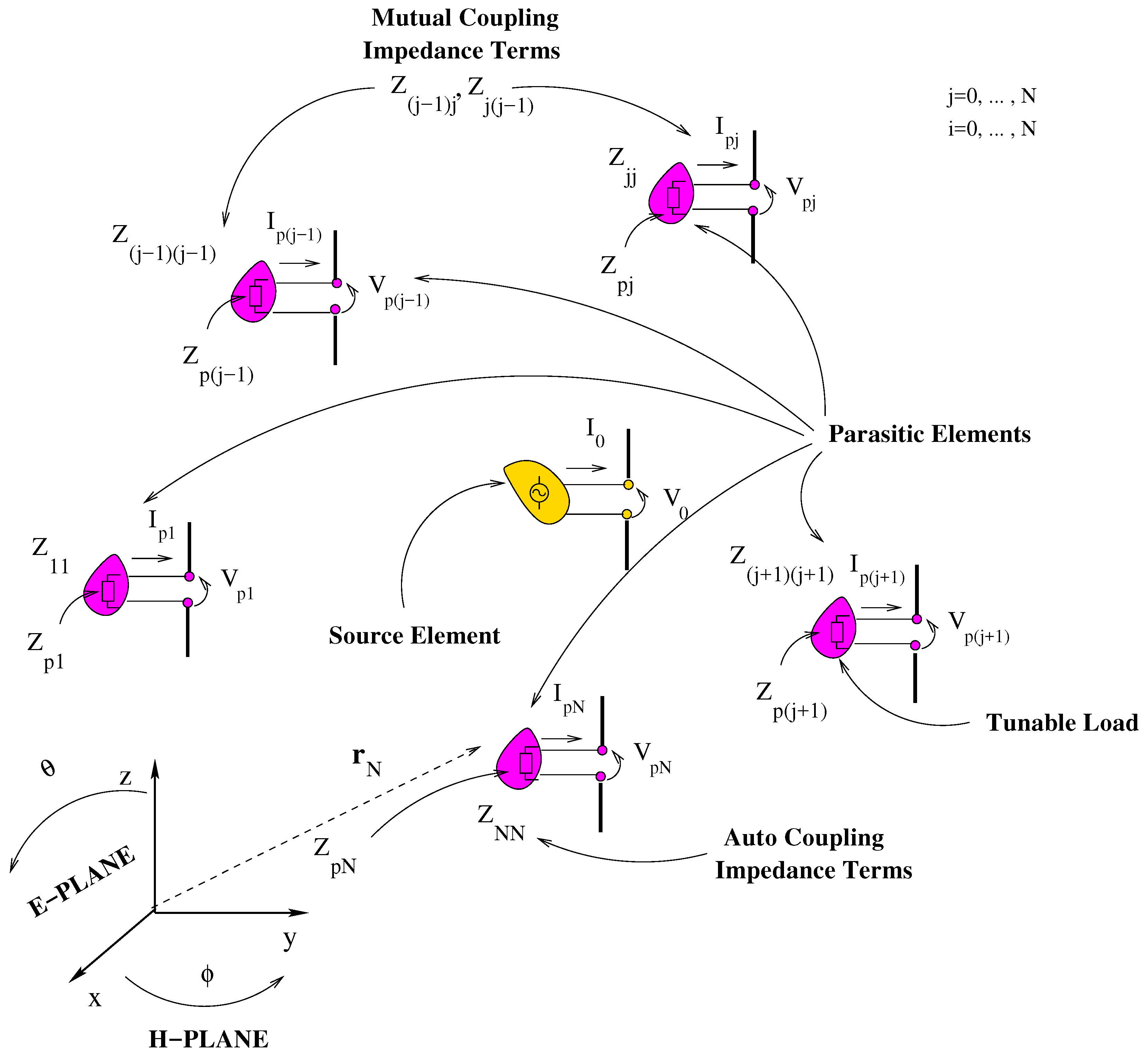
Let us consider the generic radiating structure composed of an active element surrounded by N loaded parasitic elements, as depicted in Figure 1. The active element is connected to an radio frequency (RF) receiver or transmitter and each parasitic element is loaded with an impedance . This structure can act as a reconfigurable antenna, in particular the beam patter of the active element can be controlled by opportunely varying the values of load impedances connected to the parasitic elements that surround the active element. The electrical parameters describing the behaviour of the antenna system at the input ports of the active and of the parasitic elements, shown in Figure 1, are the following voltages and current vectors provided by:
where the underscript refers to the active element. Auto and mutual impedances at the input ports of the antenna system are represented by the matrix . In particular, are the mutual impedances between elements of the structure and represent the auto impedance of the j-th element. The knowledge of the impedance matrix is mandatory in order to calculate the current values in each element of the considered structure by the following:
The computation of values is not a trivial task and usually it is performed by means of a numerical methods. Following the formulation given in [17], it is possible to obtain the H-plane pattern factor as follows:
where is the current in the active element, and , are the positions and the lengths of the linear elements of the array, respectively, and the coefficient are the values of the currents on the antenna elements, normalized with respect to . By introducing in Equation (3) the electrical conditions given by the insertion of the load impedances on the antenna parasitic elements the following system of equations is obtained:
According to (5), the coefficients () may be computed by solving the following system of equations:
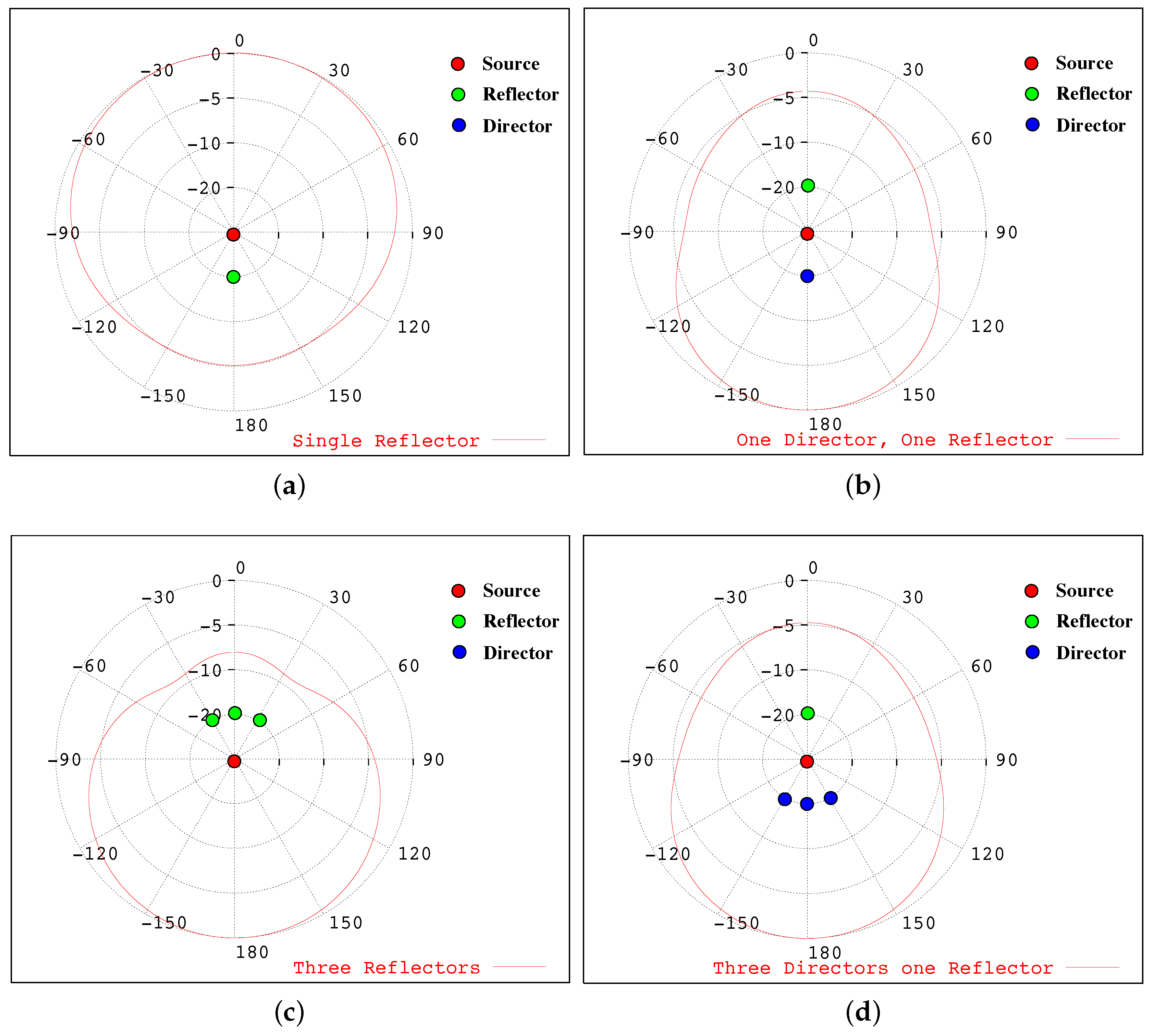
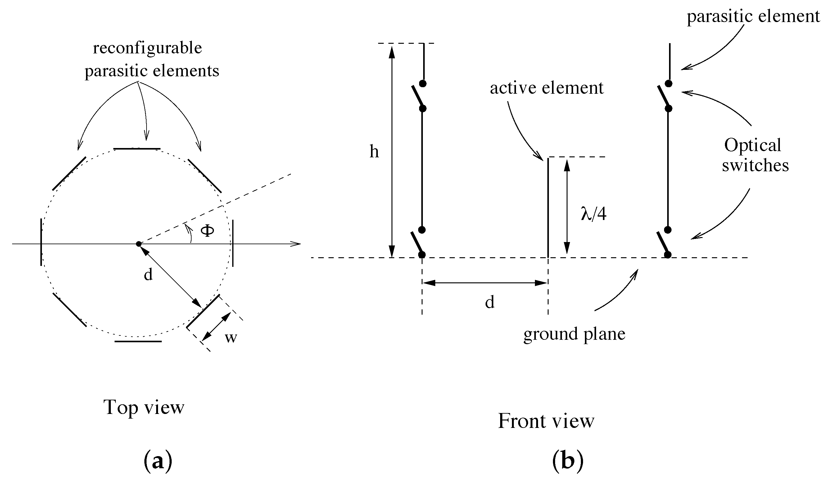
The relationships (6) show that a possible method for the control the pattern factor, given in (4), is based on the loads variations . In particular, by assuming , the contribution of the j-th element, can be neglected obtaining a disabled state of the j-th element. This function in practise may be employed in order to re-configure the pattern factor of the antenna by enabling or disabling the elements, simply adopting as loads for the parasitic elements N switches. Let us consider a reference structure based on a source dipole (the 0-th element) surrounded by N parasitic elements arranged on a circle in the plane placed in the source position and with a radius of . We assume that the N parasitic elements can be enabled or disabled by means of switches connected to their ports and, in addition, we also assume that their lengths can be varied in order to change the phase of the inducted currents, obtaining a generalized Yagi–Uda like structure whose pattern factor in the H-plane can be evaluated by means of (4). In particular, when a parasitic element is longer than its resonant length, it acts as reflector (with an inductive behaviour), while when it is shorter than its resonant length, it acts as a director (with a capacitive behaviour) [18]. In order to demonstrate that such structure possesses the degrees of freedom necessary for the reconfiguration of the pattern factor, some selected simple configurations have been considered and the resulting pattern are shown in Figure 2. In particular, Figure 2a shows the normalized pattern factor of a configuration obtained considering parasitic elements with (disabled state) and a parasitic element longer then the active one (reflector state). As it can be observed, the normalized pattern factor shows a front to back ratio of about 5 decibel (dB). According to the same technique, in Figure 2b, the normalized pattern factor of the antenna reconfigured with a shorter (director state) and a longer (reflector state) parasitic elements is shown. As can be noticed in Figure 2b, the normalized pattern factor is characterized by a front to back ratio similar to that of Figure 2a but with an improved main lobe. Finally, in Figure 2c,d, the reconfiguration capabilities of the antenna in two more complex configurations (only three reflectors (c), three directors and a reflector (d), respectively) are shown. Let us consider a more specific reference structure, as depicted in Figure 3a,b based on a monopole placed on a ground plane and surrounded by eight parasitic elements arranged on a circle centered on the monopole and having radius equal to . Each parasitic element is composed by a microstrip structure printed on a planar dielectric substrate, subdivided in two isolated metallic sections that can be reconfigured by driving two switches.
To steer the main beam in a given direction, it is necessary to set one or more parasitic elements in the main beam direction (as director), while one or more parasitic elements placed in the back (opposite) direction must be chosen as longer than resonant length (reflector). The remaining parasitic elements have to be deactivated in order to minimize the perturbations on the electromagnetic field generated by the active element, the directors and the reflectors. The antenna reconfigurability is obtained by introducing in the geometry of each parasitic element an upper switch, as shown in Figure 3b, in order to set them as director (upper switch open) or as reflector (upper switch closed), while in order to deactivate an element of the structure another switch set the (lower switch in Figure 3b open). In order to optimize the geometrical parameters of the parasitic structure, a simple configuration composed only of the source element and by two diametrically opposed parasitic elements has been considered. A detailed view of a section of the geometry of the reference configuration is given in Figure 3b where also the geometrical parameters of the structure are shown. The design of the parasitic elements configuration has been formulated as an optimization problem by defining suitable constraints on gain G, on voltage-standing-wave-ratio () and on the front to back ratio . The unknown descriptive parameters of the reference configuration have been optimized by minimizing the cost function , defined in terms of the least-square difference between requirements and estimated values of G, and :
where , d is the radius of the circular parasitic structure, w and h are, respectively, the width and height of all the planar printed parasitic element, respectively, is the height of the upper gaps from the ground plane and is the gaps thickness, and . In order to minimize (7) and, according to the guidelines reported in [19,20], a suitable implementation of the [21,22,23,24,25,26,27,28,29] and of a geometry generator, able to modify and control the reference geometrical parameters, have been integrated with a method-of-moments () [30] electromagnetic simulator. Starting from the set of trial arrays , u the trial array index, , and the iteration index, , respectively) iteratively defined by the , the geometry generator defines the corresponding reference antenna structures for computing the corresponding , gain and front to back ratio values by means of the simulator. As previously described, the reference configuration adopted for the design and optimization of the geometrical parameters of the reconfigurable antenna is composed by a quarter wave active element, a reflector, a director, placed in a diametrically opposed position, and with all the other parasitic elements in the disabled state (all the gaps opens); the presence of a reference ground plane of infinite extent is assumed. The iterative process continues until or , where , K is the maximum number of iterations and the convergence threshold. As shown in the following sections, devoted to the numerical and experimental validation of the reconfigurable antenna, in addition to the parasitic elements considered in the reference configuration (a reflector and a director), the control algorithm developed and integrated with the reconfigurable antenna can activate additional parasitic elements, as directors or reflectors, in order to increase the gain in the direction of arrival of the desired signal and at the same time to increase the attenuation in the direction of interfering signals.
3. The Antenna Design and Prototype Development
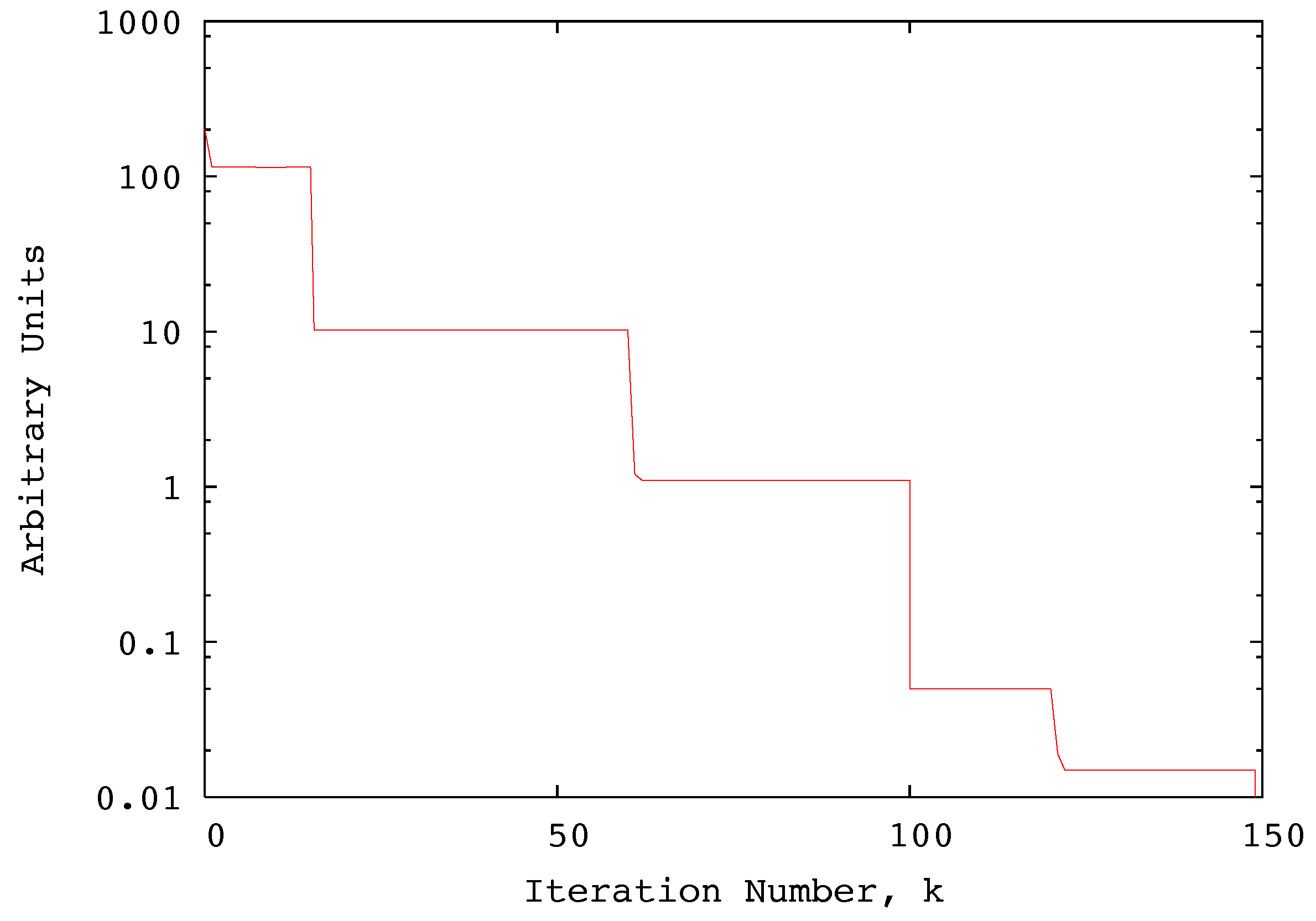
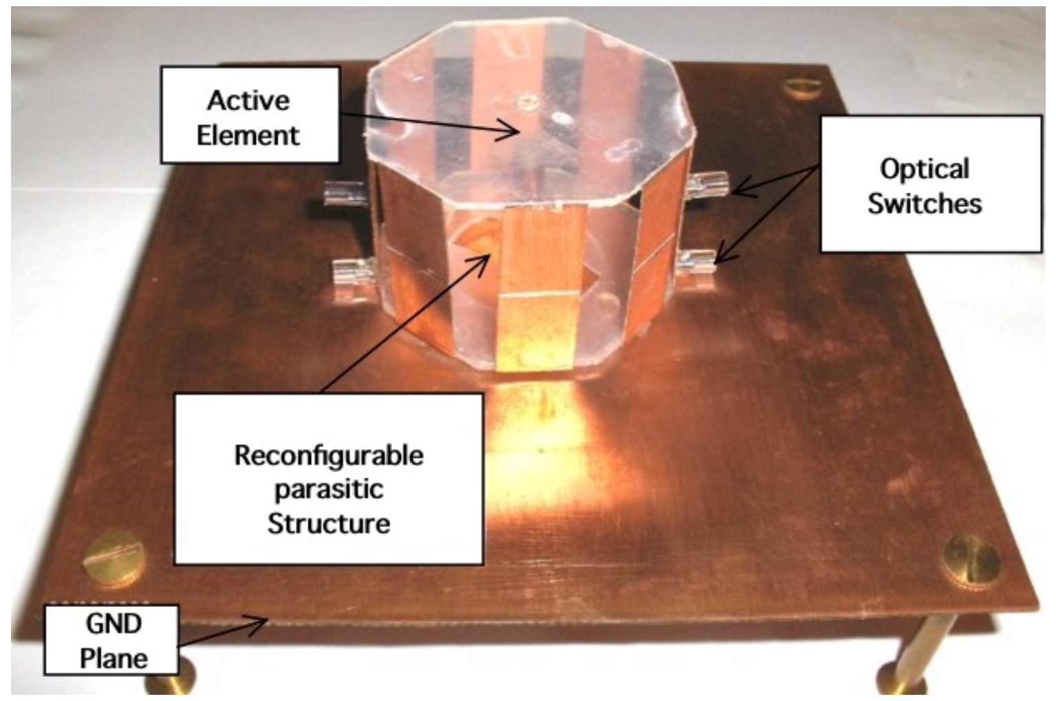
In this section, the design, the optimization and the development of a prototype of the proposed reconfigurable antenna are reported. Concerning the design and optimization procedure previously detailed, the specific PSO adopted for minimizing the cost function (7) considers a swarm of trial solutions, a maximum number of iterations and a threshold . The other parameters of the PSO have been set according to the reference literature [19,21]. The following antenna constraints in the working frequency band have been taken into account in the optimization procedure: a voltage-standing-wave-ratio , a front to back ratio and a gain dBi. In particular, the active and the parasitic elements of the antenna have been designed to work in the ISM band in the range between GHz and GHz, the active element is fabricated with a copper hollow pipe with a diameter mm, and a length m, a tuning screw mounted on the top of the monopole permits to vary the monopole length in the range in order to better tune the antenna resonant frequency. The geometrical constraints are not critical parameters because the proposed antenna is intended for automotive applications, however, in order to obtain a reasonably limited structure, a maximum volume having dimensions equal to cm has been assumed. In order to show the required computational effort, in Figure 4, the plot of the cost function versus the iteration number, recorded during the optimization process, is shown; as it can be noticed, the optimization required about iterations. According to the results of the optimization procedure (, , , , (where is the wavelength at the centre of the band), a prototype of the reconfigurable antenna has been built. As shown in the photograph in Figure 5, each parasitic element has been built by using a photo lithographic printing circuit technology, and it has been equipped with two switches, namely the SFH350 photo-transistor. The electric characteristics of the SFH350 switches have been measured by means of a network analyser aimed at measuring the impedance in the two states’ opening/closing of the switch. In particular, and in the central band GHz; however, a small variation below at the boundary of the considered frequency range. In order to minimize the perturbation of the electromagnetic behaviour of the reconfigurable antenna, the parasitic elements have been equipped with optical switches, allowing a completely dielectric driving of the reconfigurable structure. The eight parasitic elements and the active element have been assembled on a dielectric cylindrical surface, and the resulting antenna structure has been placed on a reference ground plane having dimensions equal to cm, while, during experimental activities, a ground plane of cm has been used. A photograph of the prototype during the development phase is shown in Figure 6, where only four optical switches can be observed; the prototype at this stage of the development (with optical switches only on a director and a reflector) has been employed for the experimental validation of the reference configuration, as described in the Section 3.3. As it can be noticed from the photo in Figure 6, the number of parasitic elements is , and it has been chosen considering a compromise between shielding capabilities and mechanical constraints. In particular, the number of parasitic elements cannot be increased too much due to mechanical constraints and mutual coupling effects. On the contrary, much too low M strongly decreases the antenna shielding performances. The considered number of parasitic elements has been chosen after a set of numerical and experimental tests, and offers good shielding and direction of arrival (DOA) performances and a reasonable compactness.
3.1. The Control Algorithm
As described in the previous sections, the reconfigurable antenna proposed in the paper have reconfigurable parasitic elements and an active element. By acting on two optical switches, each parasitic element can assume three different states: reflector, director or disabled. The antenna can assume different states and the antenna configurations can be represented by means of a binary vector of length 2M. The control algorithm has been designed in order to give to the reconfigurable antenna two different functionality: (a) tracking of the direction of arrival (DOA) of a signal, and (b) shielding of interfering signals. The development of the control module of the reconfigurable antenna has been done recasting the required functions as optimization problems, and, due to the discrete nature of the related search problem, a binary version of the PSO optimizer, recently experimented on by the authors for the control of planar phased arrays [7], has been adopted. The following steps summarize the application of the binary PSO strategy by focusing on its customization to the real-time control of the adaptive antenna.
- Coding.The proposed antenna prototype is controlled by means of a binary vector W of length 2M, which represents the states of the optical switches. A swarm of P particles represents a set of P trial solutions. With each position vector, is associated with a velocity vector .
- Initialization.The particles’ positions vectors as well as their velocities vectors are randomly initialized.
- Iteration updating.The iteration index is updated
- Fitness evaluation.At this step, the fitness of each particle is evaluated. Two different cost functions are considered, dependently on the operative mode considered. In particular, for DOA identification, the goal is to steer the antenna main beam in the direction of the desired signal (assuming that there aren’t co-channel interfering signals). The received power collected at the output port of the active element is used as a cost function:When a shielding operation is required, the DOA and the reference power related to the desired signal in the absence of any interfering signals is assumed to be known, so the first operation to perform is to steer the beam along the direction of the desired signal, as for DOA search, and to measure the received reference power ; the following cost function is considered:where is the received power due to the presence of interfering signals. After the evaluation of the particles’ fitness, the global and the previous best position vector [8] of the swarm are identified.
- Iteration updating.The iteration index is updated
- Termination strategy.The control algorithm is stopped when the fitness is stationary for about consecutive time-steps.
- Velocity and position updating.The velocity of each particle is updated according to the following relation:where is a clamping value [8], and is givenwhere are two constants called cognition and social acceleration, respectively, and are two positive random numbers in the range between [0:1]. The particle position is then updated as follows:where is the sigmoid function. Then, return to step 2.
3.2. Numerical and Experimental Validation
This section is aimed at the numerical and experimental of the proposed antenna prototype. The experimental results obtained with the reference configuration are compared with the corresponding numerical values; then, a selected set of experimental results, concerning different environmental conditions are presented in order to assess the capability and the current limitations of the proposed reconfigurable antenna. The beam pattern has been measured considering the central frequency GHz. The working frequency has been varied in the whole considered frequency range. The antenna beam patterns at different frequencies and operative parasitic structure configurations have been considered. The antenna performances are quite stable in the considered frequency band, demonstrating the capabilities and the efficacy of the parasitic structure. Only the active element requires a tunung by acting on the tuning screw located on the top of the active monopole. As far as the binary particle swarm optimizer (BPSO) control parameters adopted in the control algorithm are concerned, the following parametric configuration has been used: a swarm of trial configurations has been considered and , while the other PSO parameters have been chosen according to the guidelines suggested in [7].
3.3. Experimental Testing of the Reference Configuration (One Reflector and One Director)
In order to assess the optimized reference configuration, a geometry composed of a parasitic element configured as a director and another element set as a reflector in the opposite direction. The parasitic elements’ configuration has been choose to steer the main beam along a direction of degrees, while the other parasitic elements have been placed in the disabled state. Figure 6 shows the reconfigurable antenna prototype employed for the experimental activity, with the optical switches assembled only on a director and a reflector, and the other parasitic elements with all the gaps open (disabled state). The measured normalized beam-patterns reported in Figure 7 points out the capability of the antenna to steer the beam along the correct direction, in particular the main beam is positioned along the direction of the parasitic element that acts as a director, while, on the back side, along the direction of the parasitic element configured as a reflector, an attenuation of about 10 dB can be observed. For the sake of comparison, in Figure 7, the experimental results have been compared with the ones obtained with numerical simulation, in particular the numerical simulations have been performed both in the presence of the other parasitic elements in disabled state (continuous red line) and, without them, in order to verify the transparency of the parasitic structure when placed in a disabled state. As can be observed in Figure 7, the behaviour of the reference configuration isn’t modified by the presence of the deactivated parasitic elements. For completeness, also measured and computed values of VSWR, front to back (FTB) ratio, and Gain have been compared and the results are reported in Table 1. The data reported in Table 1 shows that both measured and simulated results satisfy the antenna design requirements.
3.4. Numerical Validation of the Reconfigurable Antenna
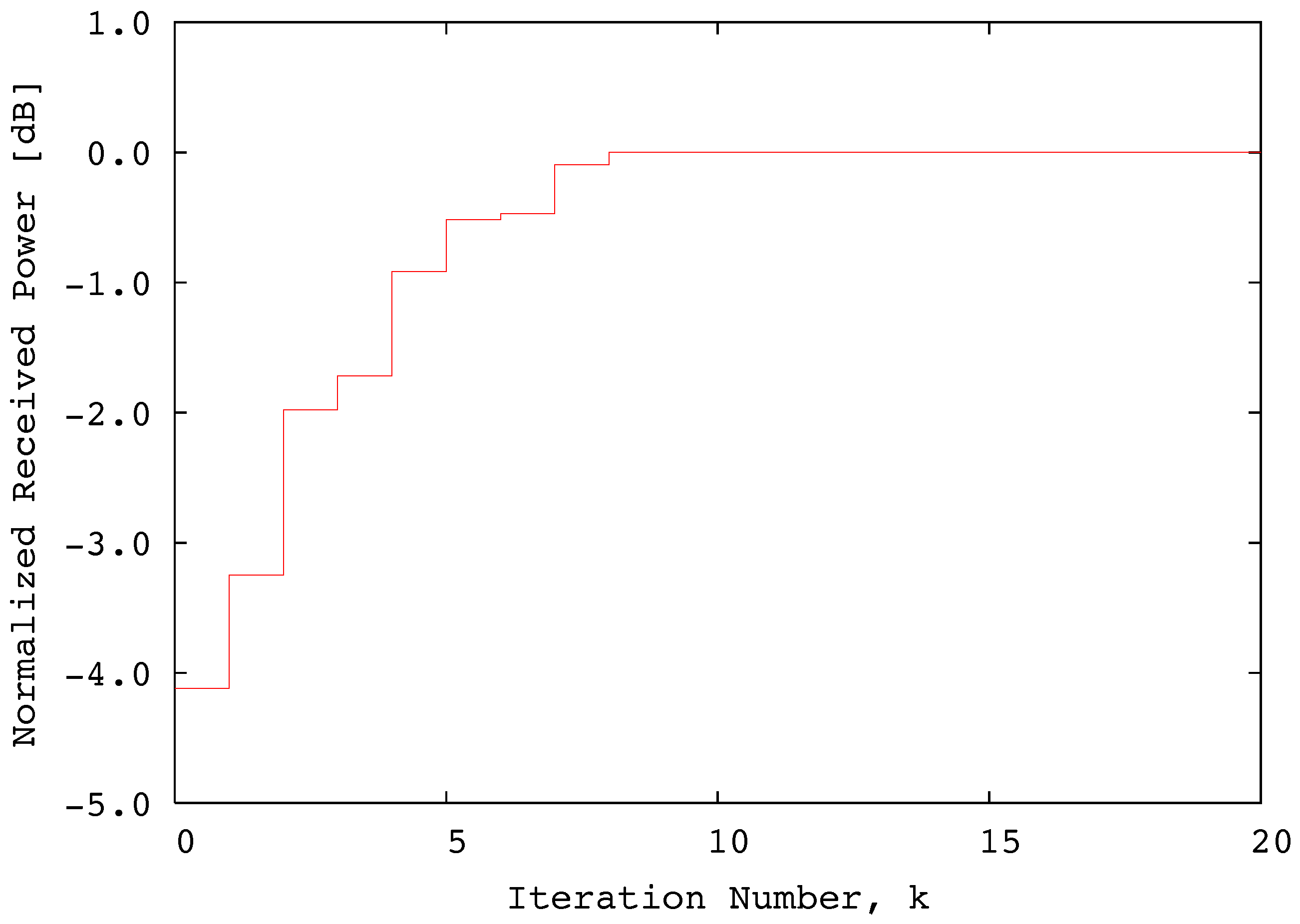
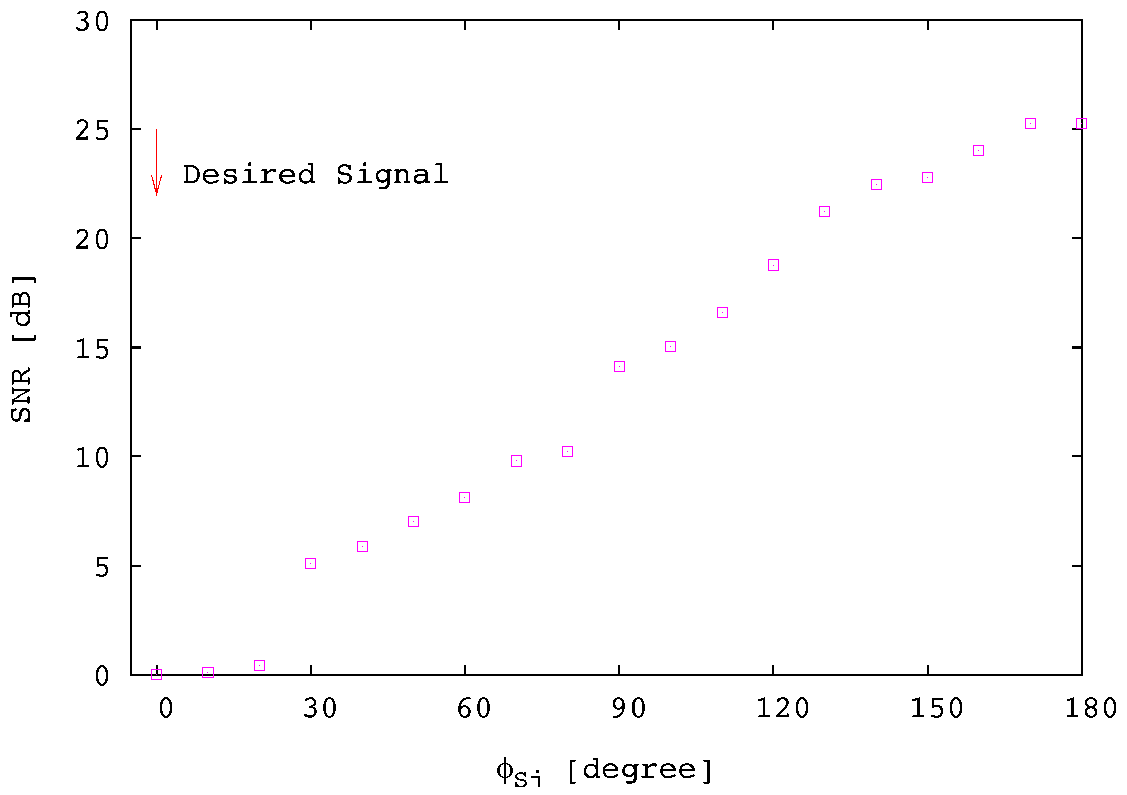
In order to test the capabilities of the proposed reconfigurable antenna and of the control algorithm, first of all, two numerical experiments have been done. To this end, the control software has been integrated with an MoM electromagnetic simulator in order to simulate the behaviour of the whole system, composed by the reconfigurable antenna and the control algorithm. The first experiment has been devoted to the identification of the DOA of a signal, which impinges on the antenna from a direction of degrees, and the considered working frequency is GHz (this frequency has been used only for the numerical validation and in order to compare the performances of the proposed antenna geometry with the results of other prototypes presented in scientific literature). The data reported in Figure 8 shows the behaviour of the cost function (8) versus the iteration number k of the control algorithm; the data of Figure 8 points out the effectiveness of the control algorithm, which is able to steer the beam of the reconfigurable antenna in the correct direction in about eight iterations. For the sake of comparison with a similar reconfigurable antenna, the obtained results have been compared with the ones experimentally obtained with the antenna prototype [11]; as it can be noticed in the normalized far-field beam pattern reported in Figure 9a, the two antennas are both able to steer the main beam in the correct direction (along ), reaching similar performances. The prototype proposed in [11], composed of 13 parasitic elements against the eight elements of the proposed antenna prototype, presents a better FTB. In the second experiment, a single interfering signal that impinges on the antenna at degrees has been considered. In this case, the considered cost function is (9) and the reference power is chosen equal to . Figure 9b shows the simulated field patterns along the plane obtained after iterations (a director and a reflector are enabled) and when the cost function become stationary for (three reflectors are activated). In Figure 9b, the far-field pattern obtained in [11] with an antenna prototype characterized by 25 parasitic elements (green line) and configured in the corresponding environmental condition is also reported. After twelve iterations of the control algorithm, the optimal antenna configuration is characterized by three different reflectors, and, in this configuration, the measured and computed values were and , respectively, the measured was against a computed value of . In the direction of the interfering signal, the antenna shows a gain of about dBi (measured) versus a computed value of dBi. Despite the limited number of parasitic elements, the proposed prototype is able to reach performances comparable with the ones obtained with the antenna characterized by twenty-five parasitic elements. In order to assess the interferences’ rejection capabilities of the antenna, several numerical experiments have been done; a desired signal impinging on the reconfigurable antenna from the direction has been assumed. As far as the interference scenario is concerned, a single interfering signal characterized with a power equal to the power of the desired signal has been considered. The direction of the interfering signal has been varied in the range from 0 up to 180 degrees. In Figure 10, the values of the signal-to-noise ratio (SNR) versus the direction of arrival (DOA) of the interfering signal is reported. As expected, when the DOA of the interfering signal is quite closer to the direction of the desired signal, the SNR value is near to 0 dB. However, when the interfering signal impinges on the antenna with a DOA far away from the direction of the desired signal, the shielding capabilities of the antenna permits achieving satisfactory values of SNR.
3.5. Experimental Validation of the Reconfigurable Antenna
The functions of the antenna prototype have been experimentally tested in a semi-anechoic chamber, and the adopted measurement set-up is shown in Figure 11. The antenna under test has been placed on a rotating platform, in order to measure the antenna far-field pattern. All the electronic devices, as the optical driver, the receiver and the analogical to digital converter were controlled by means of the control algorithm running on a personal computer. As shown in Figure 11, two different transmitting antennas allows for generating a desired signal and, at the same time, by means of an RF switch and a power splitter, to add to the scenario, also an interfering signal in the same frequency band, according to the considered test procedure described in the following.
3.5.1. DOA Identifications
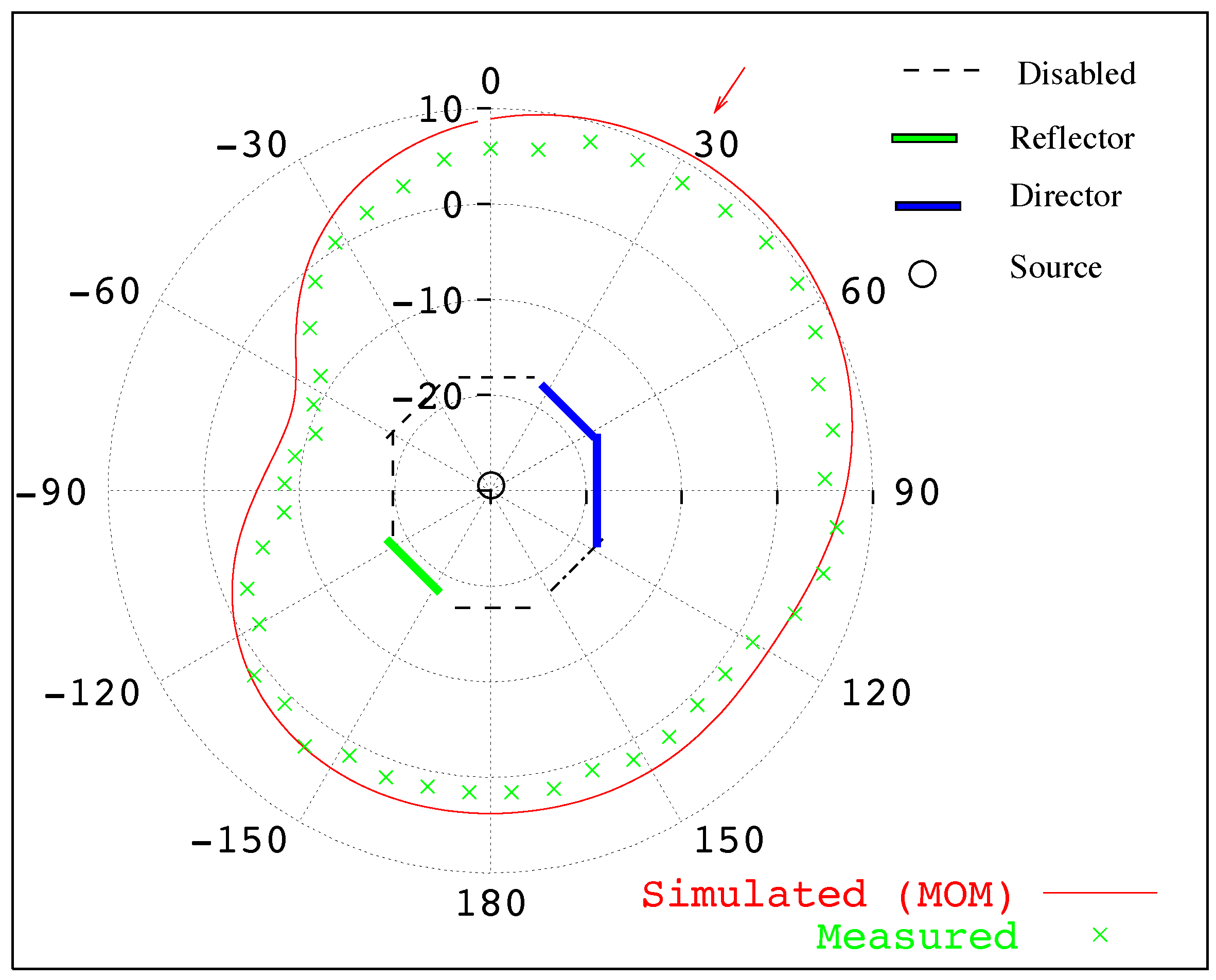
The first experimental test deals with the tracking of a signal, which impinges on the antenna from the direction , . In this first experiment, in order to emphasize the tracking capabilities of the control algorithm, no interfering signals have been considered. Figure 12 shows the measured and simulated far-field beam patterns in the H-plane. Figure 12 also shows the optimal antenna configuration, characterized by one reflector and two directors. For the sake of completeness, Table 2 reports the measured and computed VSWR, FTB ratio and Gain values. As it can be observed from the data reported in Table 2, the performances of the antenna are quite satisfactory, only the measured front to back parameter is near the limit of the imposed requirements. The second experiment concerns the tracking of a given desired signal, with a direction of arrival equal to and . The achieved antenna configuration, reached after about ten iterations of the control algorithm, is characterized by two reflectors and two directors, and it is characterized by a measured and simulated of and , respectively, a measured (the simulated value was ) and a gain of about dBi (measured) versus a computed value of dBi. As it can be observed from the field pattern reported in Figure 13, the main beam of the antenna is correctly steered along the DOA of the desired signal. The red arrow reported in Figure 13 represents the desired signal direction of arrival.
3.5.2. Interfering Signal Shielding
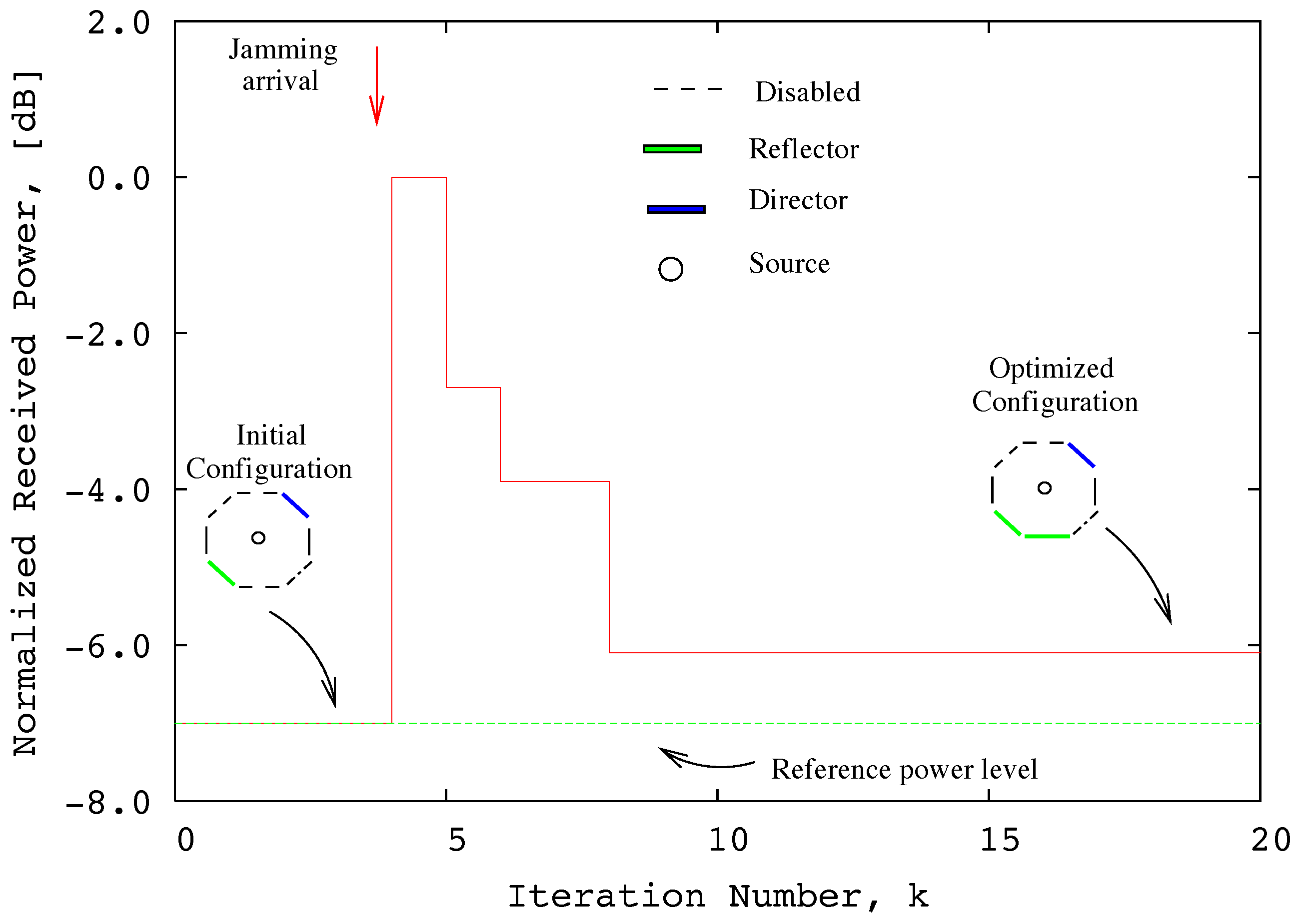
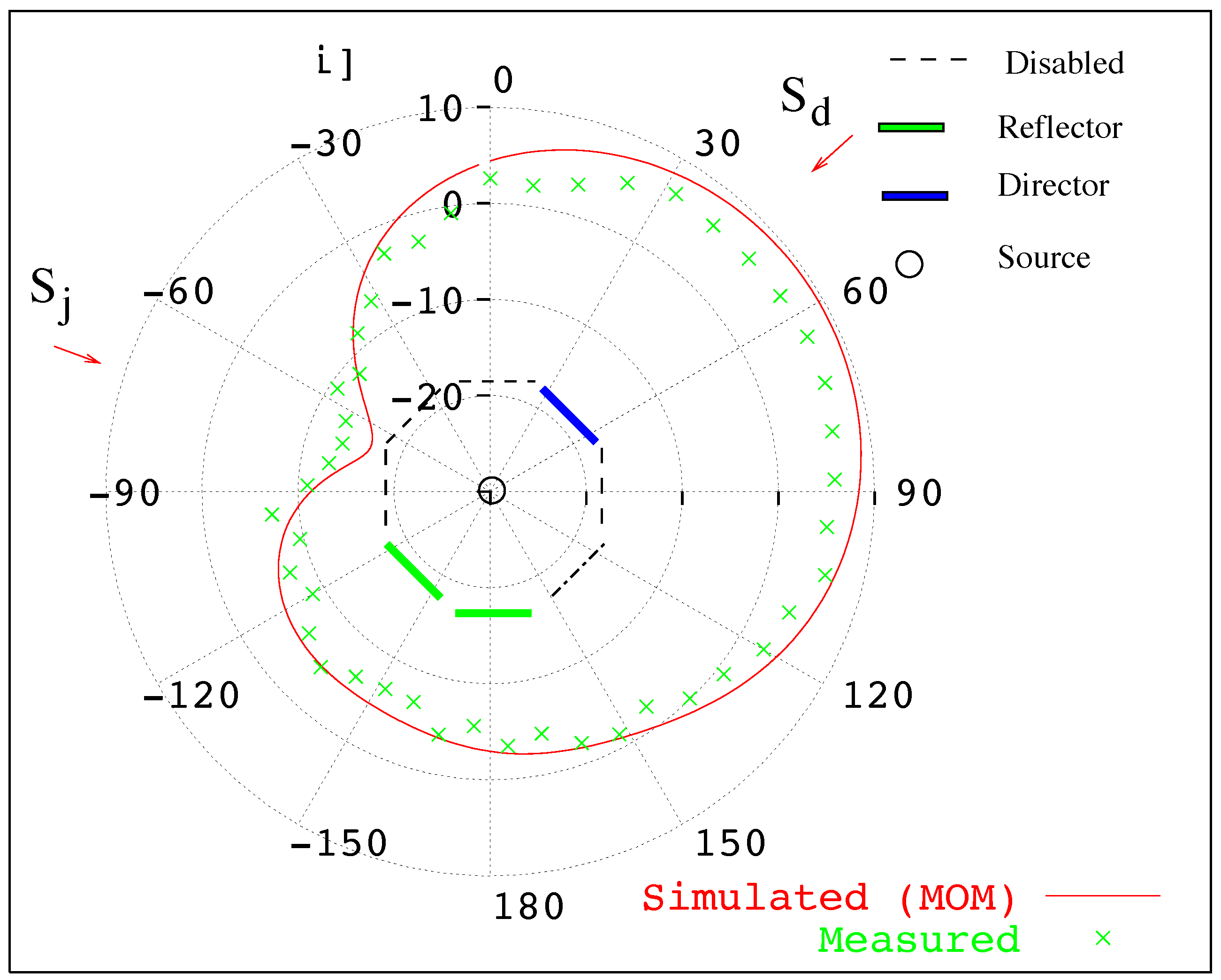
The goal of the following experiment is to assess the capability of the antenna prototype and of the control algorithm to minimize the effects of an interfering signal, which impinges on the antenna from an unknown direction. As far as the interference scenario is concerned, the power of the interfering signals is set to 20 dB above the desired signal (the power of the interference signal is 100 times greater than that of the desired signal). Without loss of generality, such a scenario has been adopted in order to allow the control software to evaluate in a simple way the effects of an interfering signals; in this simple configuration, first of all only the desired signal impinges on the reconfigurable antenna and a reference power is recorded. Then, a stronger interfering signal is activated, the control software detects a different signal to interference ratio and reconfigures the antenna in order to place a zero in the direction of arrival of the interfering signal and to recover the reference power level. In this experiment, the DOA of the desired signal and the power ratio between the desired and interfering signals are assumed known quantities. These strong hypotheses can be easily removed assuming to insert in the system a module able to detect the real signal to interference ratio. The direction of the desired and interfering signals are and , respectively. The antenna has been initially configured activating a director along the direction of the desired signal and a reflector in the backside. The received power has been measured; then, the interfering signal has been activated together with the control algorithm. Figure 14 shows the normalized measured received power at the output port of the antenna versus the iteration number of the control algorithm; as it can be noticed, after the arrival of the jammer indicated in Figure 14 by an arrow (iteration ), the control algorithm tried to keep the received power to the reference value (green line), by activating the elements of the reconfigurable structure. Figure 14 also reports the initial and the final antenna configuration. In Figure 15, the shielding capabilities of the antenna are more evident: in correspondence with the DOA of the interference signal, the field pattern shows an attenuation of about dB. In this case, the antenna parameters are kept below the requirements, in particular the measured against the computed value of , a measured (the simulated value was ), and a gain of about dBi (measured) versus a computed value of dBi.
4. Conclusions
The design, optimization and assessment of an adaptive antenna based on a reconfigurable parasitic structure has been described. The proposed antenna consists of a circular reconfigurable parasitic structure, which surrounds a quarter wave monopole (the active element). Each parasitic element of the reconfigurable structure can be optically enabled and acts as a reflector or director in order to steer the main beam in a given direction (acting like a Uda–Yagi array) or to shield the effects of an undesired interfering signal. The reconfigurable structure is driven by means of optical switches in order to limit the electromagnetic field perturbations, and it is controlled by means of a binary PSO algorithms able to choose the state of the eight parasitic elements in order to obtain the adaptivity of the antenna. The geometry of the parasitic structure has been optimized through a suitable particle swarm algorithm in order to comply the electrical requirements in the operative frequency band, as well as the geometrical constraints. An antenna prototype has been designed and built. In order to assess the effectiveness of the prototype, the reconfigurable antenna has been tested considering different operative conditions, such as signal tracking and interfering signals shielding. Numerical and experimental results demonstrated the capabilities of the proposed antenna to track a desired signal or to attenuate the effects of interfering signals.
Conflicts of Interest
The author declares no conflict of interest.
References
- Hansen, R.C. Phased Array Antennas; Wiley: New York, NY, USA, 1998. [Google Scholar]
- Applebaum, S.B. Adaptive arrays. IEEE Trans. Antennas Propag. 1976, 24, 585–598. [Google Scholar] [CrossRef]
- Widrow, B.; Mantey, P.M.; Griffiths, L.J.; Goode, B.B. Adaptive antenna systems. IEEE Proc. 1967, 55, 2143–2159. [Google Scholar] [CrossRef]
- Haupt, R.L. Phase-only adaptive nulling with a genetic algorithm. IEEE Trans. Antennas Propag. 1997, 45, 1009–1015. [Google Scholar] [CrossRef]
- Weile, D.S.; Michielssen, E. The control of adaptive antenna arrays with genetic algorithms using domunance and diploidy. IEEE Trans. Antennas Propag. 2001, 49, 1424–1433. [Google Scholar] [CrossRef]
- Donelli, M.; de Natale, F.; Lommi, A.; Massa, A. Planar antenna array control with genetic algorithms and adaptive array theory. IEEE Trans. Antennas Propag. 2004, 52, 2919–2924. [Google Scholar]
- Donelli, M.; Azaro, R.; de Natale, F.; Massa, A. An innovative computational approach based on partivle swarm strategy for adaptive phased-arrays control. IEEE Trans. Antennas Propag. 2006, 3, 888–898. [Google Scholar] [CrossRef]
- Kennedy, J.; Eberhart, R.C.; Shi, Y. Swarm Intelligence; Morgan Kaufmann: San Francisco, CA, USA, 2001. [Google Scholar]
- Dinger, R.J. Reactively steered adaptive array using microstrip patch elements at 4 GHz. IEEE Trans. Antennas Propag. 1984, 8, 848–856. [Google Scholar] [CrossRef]
- Gyoda, K.; Ohira, T. Design of electronically steearable passive array radiator (ESPAR) antennas. IEEE Antennas Propag. Soc. 2000, 2, 922–925. [Google Scholar]
- Migliore, M.D.; Pinchera, D.; Schettino, F. A simple and robust adaptive parasitic antenna. IEEE Trans. Antennas Propag. 2005, 53, 3262–3272. [Google Scholar] [CrossRef]
- De Maagt, P.; Gonzalo, R.; Vardaxoglou, Y.C.; Baracco, J.M. Electromagnetic bandgap antennas and components for microwave and (sub)millimeter wave applications. IEEE Trans. Antennas Propag. 2003, 51, 2667–2677. [Google Scholar] [CrossRef]
- Yang, F.; Rahmat-Samii, Y. Microstrip antennas integrated with electromagnetic bandgap (EBG) structures: A low mutual coupling design for arrays applications. IEEE Trans. Antennas Propag. 2003, 51, 2936–2946. [Google Scholar] [CrossRef]
- Hirata, A. Accuracy compensation in direction finding using patch antenna array with EBG structure. IEEE Antennas Wirel. Propag. Lett. 2006, 5, 1–3. [Google Scholar] [CrossRef]
- Weily, A.; Horvath, L.; Esselle, K.; Sanders, B.; Bird, T. A planar resonator antenna based on woodpile EBG material. IEEE Trans. Antennas Propag. 2005, 53, 216–223. [Google Scholar] [CrossRef]
- Boutayeb, H.; Denidni, T.A.; Mahdjoubi, K.; Tarot, A.; Sebak, A.; Talbi, L. Analysis and design of a cylindrical EBG-based directive antenna. IEEE Trans. Antennas Propag. 2006, 54, 211–219. [Google Scholar] [CrossRef]
- Thiele, G.A. Analysis of Yagi–Uda-Type Antennas. IEEE Trans. Antennas Propag. 1969, 17, 24–31. [Google Scholar] [CrossRef]
- Balanis, C.A. Antenna Theory, Analysis and Design; Wiley: New York, NY, USA, 1997. [Google Scholar]
- Robinson, J.; Rahmat-Samii, Y. Particle swarm optimization in electromagnetics. IEEE Trans. Antennas Propag. 2004, 52, 397–407. [Google Scholar] [CrossRef]
- Caorsi, S.; Donelli, M.; Lommi, A.; Massa, A. Location and imaging of two-dimensional scatterers by using a particle swarm algorithm. J. Electromagn. Waves Appl. 2004, 18, 481–494. [Google Scholar] [CrossRef]
- Azaro, R.; De Natale, F.; Donelli, M.; Massa, A.; Zeni, E. Optimized design of a multi-function/multi-band antenna for automotive rescue systems. IEEE Trans. Antennas Propag. Soc. 2006, 54, 397–400. [Google Scholar]
- Luo, Y.; Chu, Q.-X.; Bornemann, J. Enhancing cross-polarisation discrimination or axial ratio beamwidth of diagonally dual or circularly polarised base station antennas by using vertical parasitic elements. IET Microw. Antennas Propag. 2017, 11, 1190–1196. [Google Scholar] [CrossRef]
- Farzami, F.; Khaledian, S.; Smida, B.; Erricolo, D. Pattern-Reconfigurable Printed Dipole Antenna Using Loaded ParasiticElements. IEEE Antennas Wirel. Propag. Lett. 2017, 16, 1151–1154. [Google Scholar] [CrossRef]
- Buckley, J.L.; McCarthy, K.G.; Loizou, L.; O’Flynn, B.; O’Mathuna, C. A Dual-ISM-Band Antenna of Small Size Using a Spiral Structure with Parasitic Element. IEEE Antennas Wirel. Propag. Lett. 2016, 15, 630–633. [Google Scholar] [CrossRef]
- Jusoh, M.; Sabapathy, T.; Jamlos, M.F.; Kamarudin, M.R. Reconfigurable Four-Parasitic-Elements Patch Antenna for High-Gain Beam Switching Application. IEEE Antennas Wirel. Propag. Lett. 2014, 13, 79–82. [Google Scholar] [CrossRef]
- Rocca, P.; Donelli, M.; Oliveri, G.; Viani, F.; Massa, A. Reconfigurable sum-difference pattern by means of parasitic elements for forward-looking monopulse radar. IET Radar Sonar Navig. 2013, 7, 747–754. [Google Scholar] [CrossRef]
- Donelli, M.; Azaro, R.; Fimognari, L.; Massa, A. A Planar Electronically Reconfigurable Wi-Fi Band Antenna Based on a Parasitic Microstrip Structure. IEEE Antennas Wirel. Propag. Lett. 2007, 6, 623–626. [Google Scholar] [CrossRef]
- Viani, F.; Lizzi, L.; Donelli, M.; Pregnolato, D.; Oliveri, G.; Massa, A. Exploitation of parasitic smart antennas in wireless sensor networks. J. Electromagn. Waves Appl. 2010, 24, 993–1003. [Google Scholar] [CrossRef]
- Donelli, M.; Febvre, P. An inexpensive reconfigurable planar array for Wi-Fi applications. Prog. Electromagn. Res. C 2012, 28, 71–81. [Google Scholar] [CrossRef]
- Harrington, R.F. Field Computation by Moment Methods; Robert E. Krieger Publishing Co.: Malabar, FL, USA, 1987. [Google Scholar]
Figure 1.
Problem geometry.

Figure 2.
Beam pattern for different parasitic structure configurations. (a) single reflector; (b) single reflector and director; (c) three reflectors; (d) three directors and one reflector.
Figure 2.
Beam pattern for different parasitic structure configurations. (a) single reflector; (b) single reflector and director; (c) three reflectors; (d) three directors and one reflector.

Figure 3.
Beam pattern for different parasitic structure configurations. (a) top view; (b) side view.
Figure 3.
Beam pattern for different parasitic structure configurations. (a) top view; (b) side view.

Figure 4.
Antenna design, optimization process. Behaviour of the cost function vs. iteration number.
Figure 4.
Antenna design, optimization process. Behaviour of the cost function vs. iteration number.

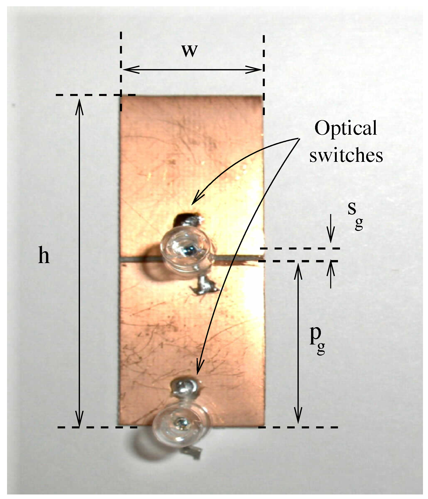
Figure 5.
Photograph of a single parasitic element of the reconfigurable antenna, with optical switches assembled.
Figure 5.
Photograph of a single parasitic element of the reconfigurable antenna, with optical switches assembled.

Figure 6.
Photograph of the antenna prototype.

Figure 7.
Numerical assessment, reference configuration one reflector and one director. Comparisons between numerical results (red line) and measured data, with parasitic elements disabled (blu cross) and completely removed (red cross).
Figure 7.
Numerical assessment, reference configuration one reflector and one director. Comparisons between numerical results (red line) and measured data, with parasitic elements disabled (blu cross) and completely removed (red cross).
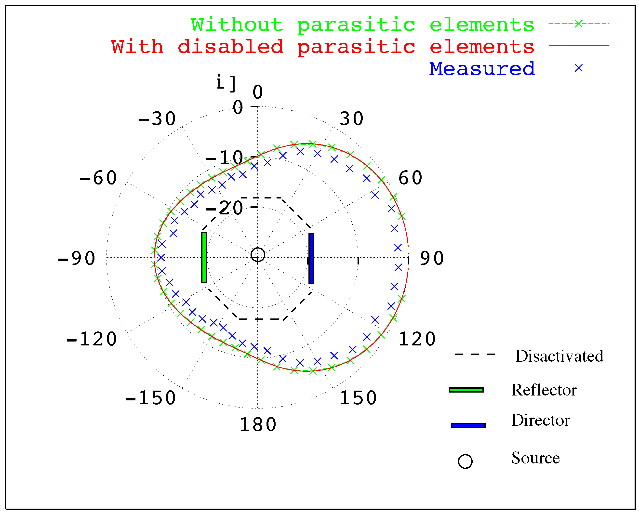
Figure 8.
Behaviour of the received power versus iteration number of the control algorithm.

Figure 9.
Numerical assessment. Direction of arrival identification, (a) desired and (b) interfering signal (. Beam pattern along plane.
Figure 9.
Numerical assessment. Direction of arrival identification, (a) desired and (b) interfering signal (. Beam pattern along plane.
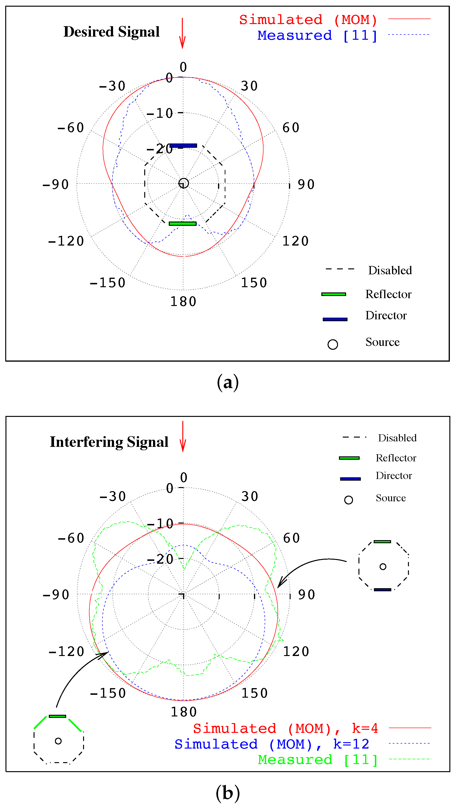
Figure 10.
Numerical assessment. Signal-to-noise ratio versus different interfering signals.

Figure 11.
Experimental assessment for multiple interfering signals scenario. Experimental set-up.
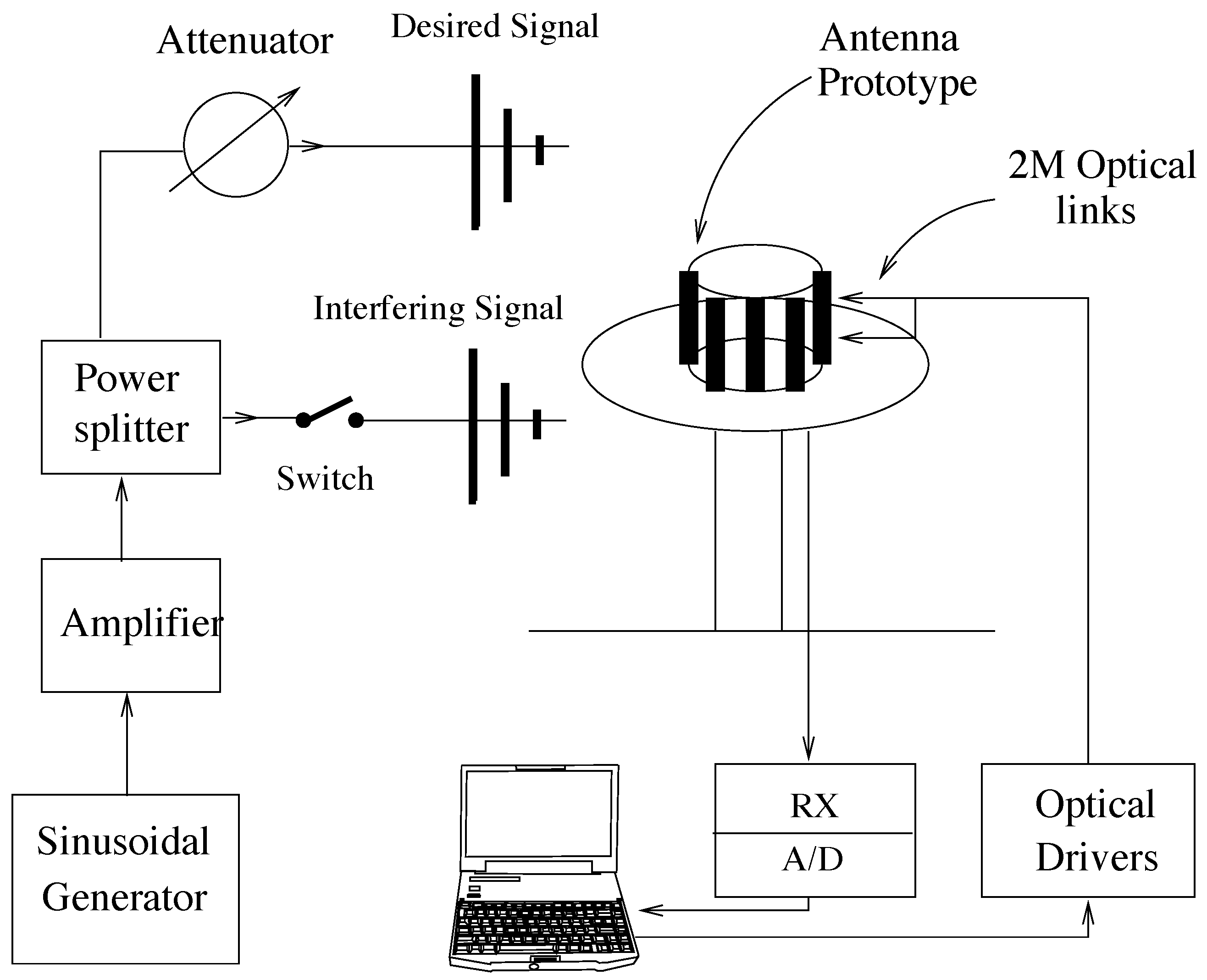
Figure 12.
Experimental assessment. Single desired signal, impinging direction (). Beam-pattern ( plane.
Figure 12.
Experimental assessment. Single desired signal, impinging direction (). Beam-pattern ( plane.

Figure 13.
Experimental assessment. Single desired signal, tracking example, impinging direction (). Beam-pattern ( plane.
Figure 13.
Experimental assessment. Single desired signal, tracking example, impinging direction (). Beam-pattern ( plane.
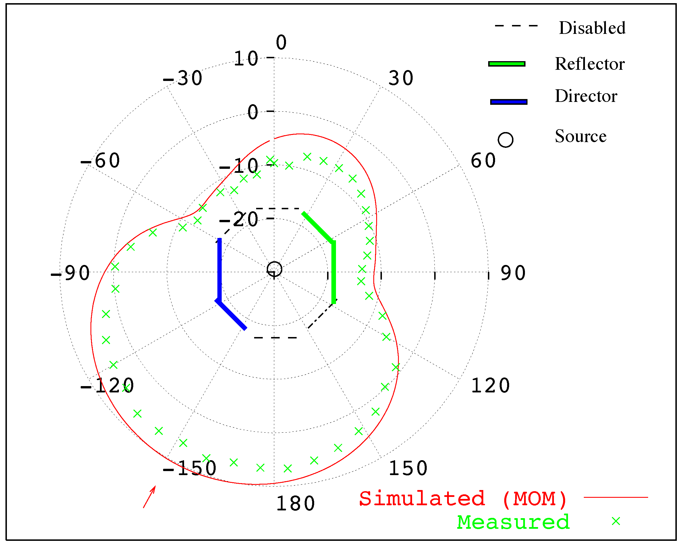
Figure 14.
Experimental assessment. Single interfering signal scenario. Behaviour of the normalized receiving power versus iteration number.
Figure 14.
Experimental assessment. Single interfering signal scenario. Behaviour of the normalized receiving power versus iteration number.

Figure 15.
Experimental assessment. Single interference signal, tracking example, impinging direction (, ). Beam-pattern ( plane.
Figure 15.
Experimental assessment. Single interference signal, tracking example, impinging direction (, ). Beam-pattern ( plane.


Table 1.
Numerical assessment. Comparisons between computed and measured antenna parameters, with enabled and disabled parasitic elements.
Table 1.
Numerical assessment. Comparisons between computed and measured antenna parameters, with enabled and disabled parasitic elements.
| Enabled Parasitic Elements | Disabled Parasitic Elements | Measured | Requirements | |
|---|---|---|---|---|
| VSWR | 1.42 | 1.43 | 1.51 | <2 |
| FTB | 11.0 dBi | 11.0 dBi | 9.0 dBi | >8 dBi |
| Gain | 10.0 dBi | 10.1 | 8.1 dBi | >5 dBi |
Table 2.
Experimental assessment. Comparison between computed and measured antenna parameters.
| Computed | Measured | Requirements | |
|---|---|---|---|
| VSWR | 1.72 | 1.83 | <2 |
| FTB | 9.0 dBi | 8.2 dBi | >8 dBi |
| Gain | 11.0 dBi | 7.0 dBi | >5 dBi |
© 2018 by the author. Licensee MDPI, Basel, Switzerland. This article is an open access article distributed under the terms and conditions of the Creative Commons Attribution (CC BY) license (http://creativecommons.org/licenses/by/4.0/).
Share and Cite
MDPI and ACS Style
Donelli, M. A Simple and Efficient Adaptive ISM-Band Antenna Based on a Reconfigurable Optically Driven Parasitic Structure. Electronics 2018, 7, 21. https://doi.org/10.3390/electronics7020021
AMA Style
Donelli M. A Simple and Efficient Adaptive ISM-Band Antenna Based on a Reconfigurable Optically Driven Parasitic Structure. Electronics. 2018; 7(2):21. https://doi.org/10.3390/electronics7020021
Chicago/Turabian StyleDonelli, Massimo. 2018. "A Simple and Efficient Adaptive ISM-Band Antenna Based on a Reconfigurable Optically Driven Parasitic Structure" Electronics 7, no. 2: 21. https://doi.org/10.3390/electronics7020021
Note that from the first issue of 2016, this journal uses article numbers instead of page numbers. See further details here.