1. Introduction
The aim of motion detection systems (MDS) is the detection of the movement of scattering objects. MDS are normally used for security purpose, such as to protect indoor areas, and locations where important assets are located (museums, libraries), or in automotives to avoid car collisions. The detection of a movement usually triggers an alarm, or, more generally, activates other electronic subsystems.
MDS use different methods to detect movement, and can be divided into two main categories: passive detectors and active detectors. Passive detectors (for example, most infrared detectors) do not send out signals but merely receive signals, such as changes in brightness temperature, light intensity and so on. On the other hand, active detectors (such as microwave detectors) act as a radar, i.e., they transmit energy that propagates in the protected area, it is scattered by the existing bodies, and then it is received back by the MDS. In this case, for example, an alarm can be triggered by any perturbation of the reflected waves caused by a moving object or by any movement of a body with a Radar Cross Section (RCS) larger than a prescribed threshold (e.g., to detect humans but prevent the detection of mice). A block diagram of a microwave MDS is shown in
Figure 1. The microwave part of the MDS is made by a voltage-controlled oscillator, a low pass filter, a transmitting and a receiving antenna, a mixer and a directional coupler. The directional coupler is required to perform coherent detection of the received signal, thus allowing a larger receiver sensitivity and then a larger detection range. Thus, this coupler requires both strong coupling and large isolation. On the other hand, it should be compact and low-cost. As such, the directional coupler is one of the most critical components of a microwave MDS.
In this paper we focus on the design of the directional coupler employed to feed the mixer for the “MURENA” Doppler motion detection sensor (DMDS) [
1]. MURENA is a volumetric X band microwave sensor, using the Doppler effect and digital signal processing, for external protection. Like all sensors using microwave technology to detect motion, MURENA exploits the principle of a Doppler radar, where a continuous wave of microwave radiation is emitted by a RF source. The frequency shift in the reflected waves, due to the motion of an object toward (or away from) the receiver, results in a signal at low frequency. The MURENA interface between the microwave transmitter–receiver is designed using a special circuit, which generates a modulation signal on the transmitter, demodulating and pre-amplifying the received signal using two separate channels. This performance is then enhanced by subsequent signal processing which, after amplification, is digitized using an analogue/digital convertor. This digital signal is handled in real time by the on-board microprocessor. Using appropriate algorithms it is possible to measure the distance and the mass of the object moving within the detection area, analyzing all the received data using a “fuzzy” logic.
Figure 1 reports a block diagram of the whole sensor. The mixer used in this system is a single balanced 180° “rat-race” type, which, in order to work properly, requires a DC-isolated directional coupler with a large coupling, typically larger than −7 dB. The operating frequency range, 10–11 GHz, was chosen to comply with different national regulations.
The most popular configuration of a directional coupler is the standard coupled-line directional coupler (SC) [
2,
3,
4], which allows the realization of quite a compact coupler with good bandwidth. Moreover, the coupled port is DC isolated from the through line. On the other hand, the strongest coupling factor of a standard coupler realization is limited to about 9–10 dB [
2]. Such values are too small for our application (and for many similar applications). Increasing the coupling requires very close coupling lines, which can be realized only using high-cost processing over expensive PCB [
5]. As an alternative, stronger coupling factors can be obtained with more complex (and bigger) structures, such as the Lange coupler [
2], or other special techniques [
6,
7], not compatible with the system target price. Therefore, a compact coupler configuration, able to realize a relatively strong coupling factor, with low-cost material and technology (and therefore using large inter-line spacing), such as those needed by a MDS, requires a different configuration.
Simple and compact coupler configurations, based on the asymmetric cascade connection of two coupled line sections, are proposed in [
8] in the lower UHF frequency band (600 MHz) in order to improve flexibility in the design of couplers for complex circuit environments, within a limited area. In this paper, we use essentially the same configuration presented in [
8], but for a different purpose, i.e., in order to achieve tight coupling and high directivity, compared to the SC [
2], in the X frequency band, using low-cost materials and technology. However, the improvement is not straightforward, since increasing the coupling factor using low-cost material in a far higher frequency range, where dielectric and ohmic losses could be critical, can be challenging. We will demonstrate that the selected configuration is able to strengthen the coupling factor over that of a SC with the same inter-line spacing. This improvement is obtained at the expense of the total coupler size. However, as shown in
Section 3, this size increase does not significantly affect the coupler loss efficiency. In fact, in our case, the actual coupling region increases only by 10% compared to the SC (from 90° to 100°).
The design of the directional coupler was performed through a simplified circuital model, and then optimized by using the commercial software HFSS by Ansys. A prototype has been realized by R&D Labs of CIAS Elettronica, using a low-cost laminate. Measured results on the realized prototype are in very good agreement with simulations, allowing the achievement of the coupling factor required by the design specifications. The proposed directional coupler was also compared with a SC with the same inter-line spacing, showing its ability to increase the coupling factor.
2. Analysis of the Proposed Configuration
The scheme of the proposed coupler is shown in
Figure 2a. Networks A and D are two equal coupled line sections (CLSs) acting as directional couplers with port impedances Z
0 = 50 Ω, whereas B and C are microstrip transmission lines with characteristic impedances Z
0. Let
ϑB and
ϑC denote the electrical lengths of the transmission lines B and C;
ϑB should be equal to the required spacing between the two CLSs, whereas
ϑC is usually chosen to be longer than
ϑB, as line C can be realized as a meander line. The microstrip realization of the proposed coupler is reported in
Figure 2b.
Since we are interested in achieving the strongest coupling factor available, the inter-line spacing S is the smallest spacing compatible with the chosen technology. Then, the matching condition
(ZeZo)/(Zo2) = 1 [
2] must be enforced, wherein
Ze,
Zo are the even and odd mode impedances of the coupled line section. As a consequence, the width W (see
Figure 2b) is also completely determined [
2].
We further assume, for the moment, that the CLSs are ideal, i.e., that the propagation constants of both the even and the odd mode are equal, and we denote this constant by
βC. In this case, we have all ports matched and an infinite isolation over the whole frequency range [
2].
Letting
ϑA = βCLA be the electrical length of the first CLS, its scattering matrix can be obtained by [
2]
where
k = (Ze −
Zo)/(Ze +
Zo) is the maximum of the coupling coefficient
S31 achieved for
ϑA = π/2. Then, the total coupling factor of the coupler in
Figure 2 is derived in ([
8], Equation (4)), and can be written as
Now,
k is determined by the CLS geometry, so
C is only a function of
ϑA and of
ϑB +
ϑC. Therefore, the individual lengths
ϑB and
ϑC can be chosen to cope with the size requirements. In
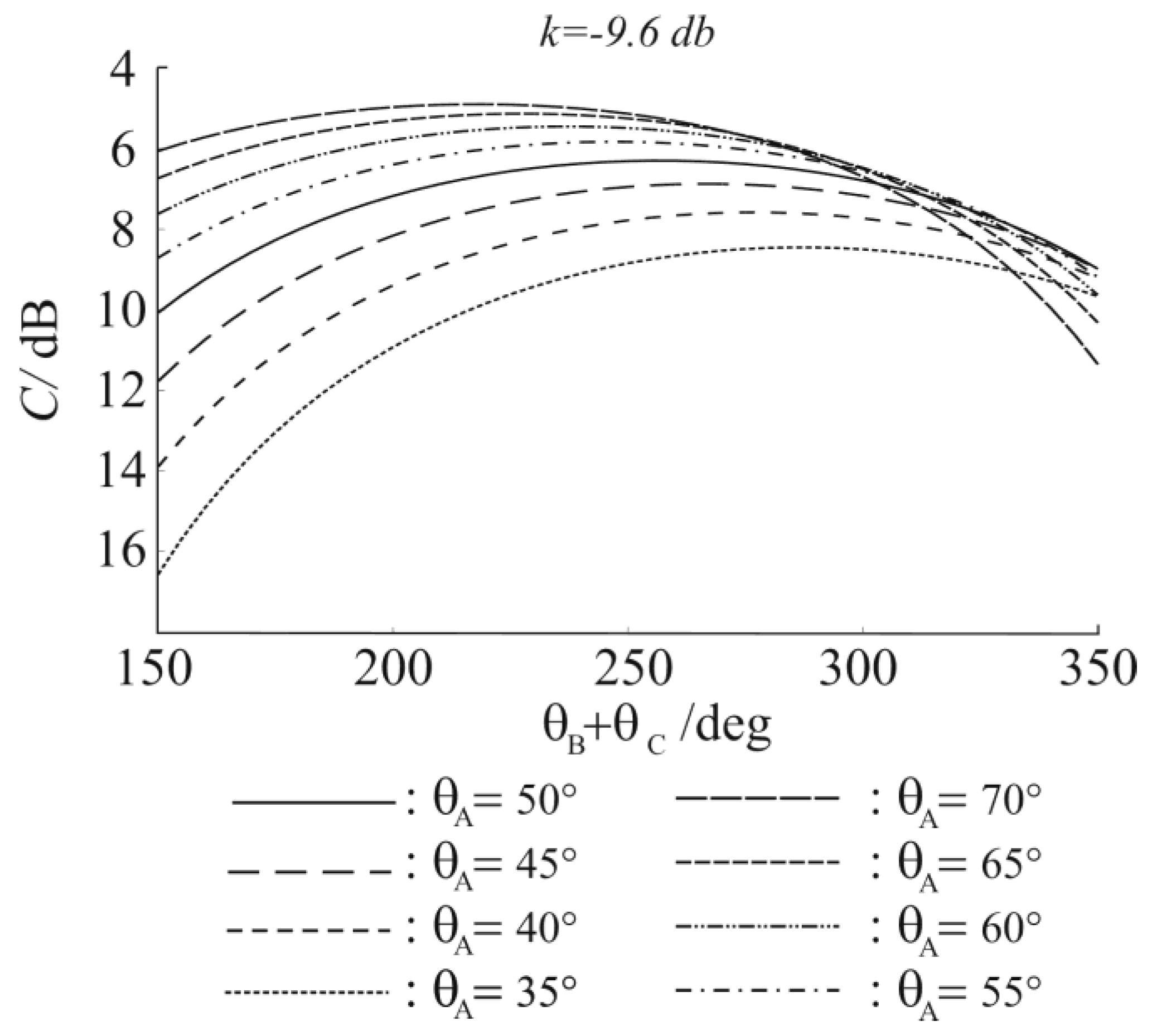
Figure 3 we show the behavior of
C as a function of
ϑB +
ϑC (for different
ϑA values) for
k = −9.6 dB. From the results in
Figure 3, it follows that the optimal value of
ϑB +
ϑC is around 280° for short CLSs, and becomes smaller as the length of the CLS increases. Moreover, the longer the
ϑA, the stronger the optimal coupling factor.
3. Coupler Design and Testing
The proposed coupler can be used in many different microwave systems. However, in order to experimentally assess the proposal, we decided to realize and test a coupler to be used in X-band DMDS. The requirements are therefore a strong coupling (C ≥ −7 dB) between the through line and the coupling port over the bandwidth 10–11 GHz, using a low-cost PCB and process. Therefore, we selected an organic–ceramic laminate, with εr = 3.5 and tan(δ) = 0.003. The dielectric slab thickness was 0.762 mm and the copper thickness was 35 μm. The smallest spacing available on this PCB with a standard (cheap) process was 0.15 mm, and this value was used for the gap S between the coupled lines.
Using [
9], the matching condition (
ZeZo)/(Zo2) = 1 results in
W = 1.4 mm. Then, the even and odd impedances (computed using HFSS) are
Ze = 69.8 Ω,
Zo = 35.2 Ω, leading to
k = −9.6 dB.
The main available degree of freedom is the length
ϑA of the CLSs. It is apparent from
Figure 3 that the longer the
ϑA, the larger both C and the increase in coupling,
C/k. However, increasing ϑ
A produces larger losses in the CLSs and a trade-off is required between
C/k on the one hand, and total coupler size and losses on the other. We selected
ϑA = 50° as a value, giving
C/k = 3.3 dB, aiming at C ≥ −7 dB over the operating bandwidth. From
ϑA = 50° and choosing
ϑB = 90°, we get, from
Figure 3, the starting value of
ϑC = 160°.
An optimization is then needed for
ϑC (i.e., on
LC2 in
Figure 2, since
LC1 is fixed by
LB) to compensate for losses and second-order effects. As a matter of fact, the bend angles of the meander line (α
C2) and the bends towards the coupler ports (α
F1) also need to be optimized (see
Figure 2). Moreover, in order to avoid the tapering of the microstrip lines
B and
C in connection with the CLSs (
W = 1.4 mm, whereas a 50 Ω microstrip line has width
W0 = 1.7 mm), in the optimized configuration these lines were selected with the same width
W = 1.4 mm as the CLSs. Since this value corresponds to a characteristic impedance of about 56 Ω, we can assume that this approximation does not affect the required coupler behavior.
To perform the optimization, the coupler of
Figure 2a was simulated using HFSS. The optimization parameters are: L
C2, the angles α
C2 (determining the electrical length ϑ
C), and the angles α
F1 of the bends in the feeding lines. The geometrical parameters of the optimized geometry, obtained after a short trial and error procedure on
LC2, α
C2, and α
F1, are summarized in
Table 1 (optimized parameters are in bold). The last bend in the feeding lines, before each feeding port, must leave room for the soldering of SMA PCB connectors, whereas the length
LF2 (= 3 mm) was to be as short as possible, provided that it did not affect the coupler behavior.
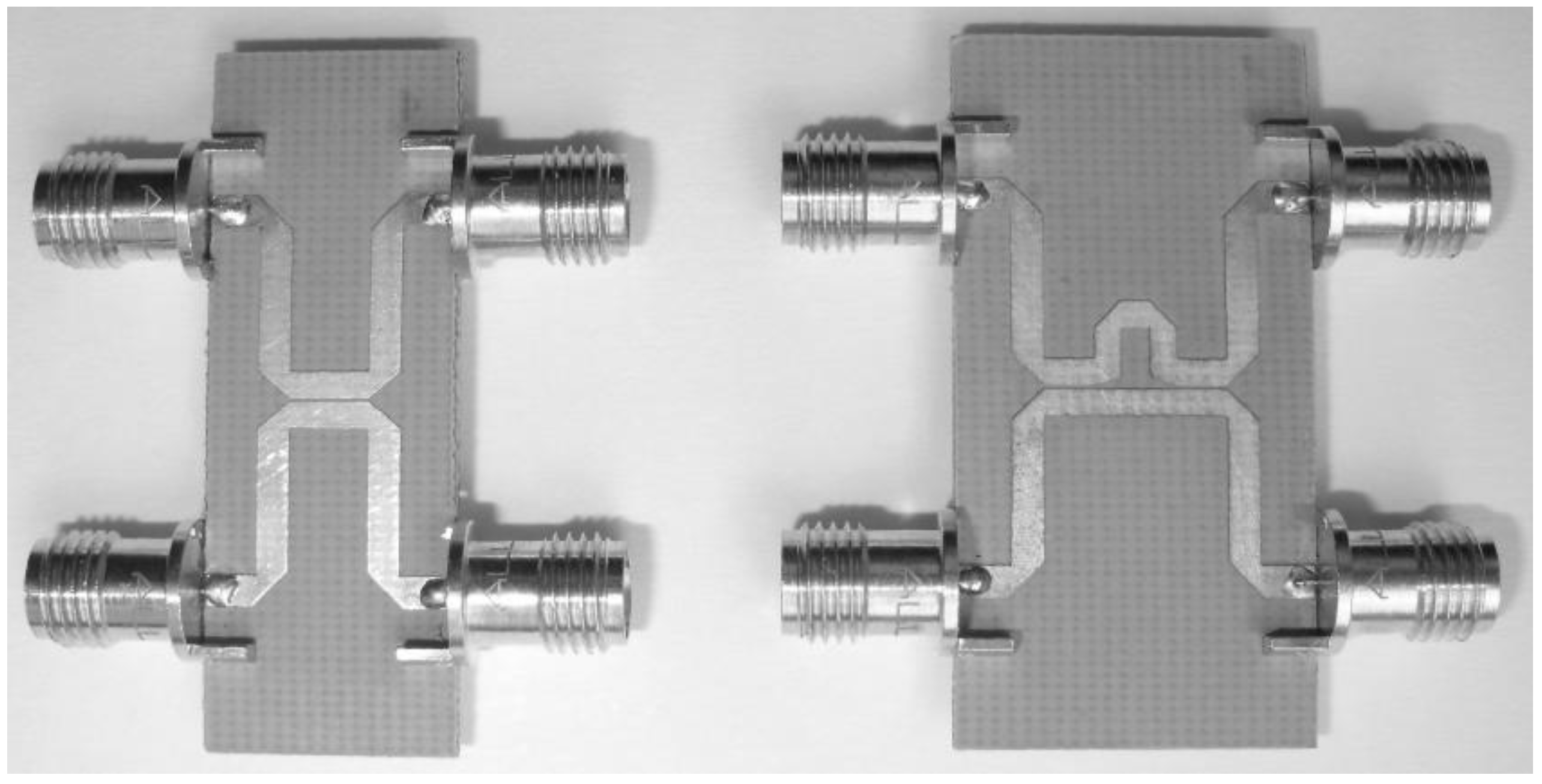
A prototype of the designed coupler was realized by the R&D Labs of CIAS Elettronica (see
Figure 4, right). For comparison, a SC with the same inter-line spacing S was also realized (
Figure 4, left). In
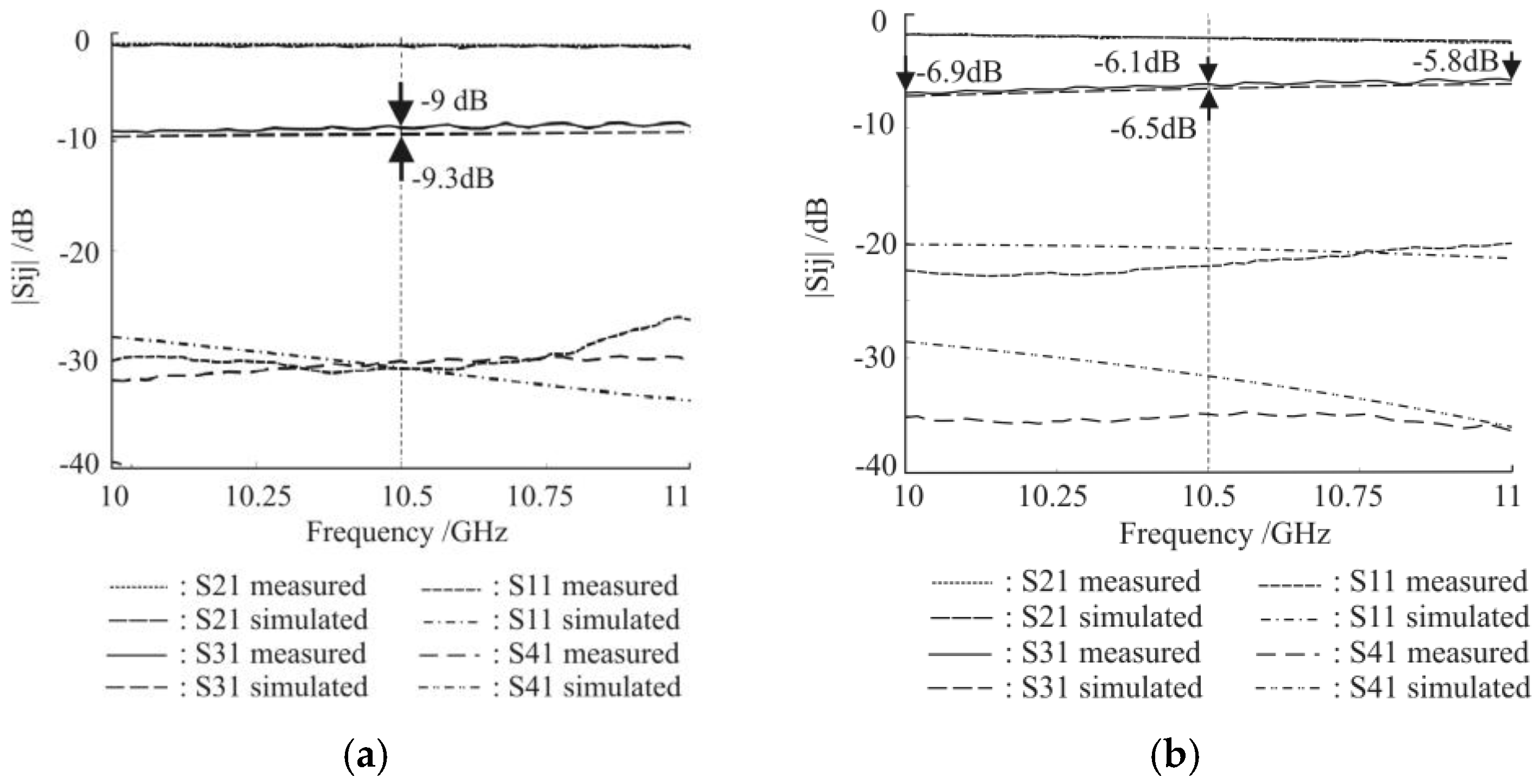
Figure 5 the simulated (HFSS) and measured frequency response of the couplers in
Figure 4 are reported. The agreement between the simulated and experimental data is very good for both prototypes.
From the results in
Figure 5b it appears that the response of the directional coupler in
Figure 4 (right) is coherent with the simplified analysis based on Equation (3) and fully complies with the design specifications, since C ≥ −7 dB in the operating bandwidth. Moreover, the resulting coupling factor at the center frequency (6.1 dB—measured data) is about 2.9 dB stronger than the standard quarter-wave coupler on the same PCB and with the same inter-line spacing (see
Figure 5). From
Figure 5, it also follows that the directivity (measured data) of the proposed coupler (28–30 dB in the operating bandwidth) is about 7 dB larger than the directivity of the SC. Therefore, the initial hypothesis on the equality of the phase velocities can be accepted, and no compensation for the difference in those speeds is needed [
10].
Finally, we wanted to evaluate the loss efficiency of the modified coupler in
Figure 2 compared to a SC. In order to do this, we observe that, for a lossless network, the dot product of any column of its scattering matrix with the conjugate of that column is equal to one [
2]. Therefore, the loss efficiency can be computed evaluating how much the parameter
η, defined as
, deviates from unity. In
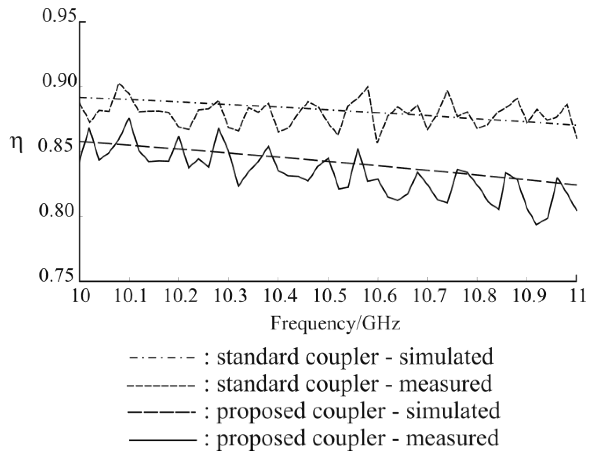
Figure 6, we plot the parameter
η for both the modified and the standard coupler. The average
η over the bandwidth 10–11 GHz for the SC is about 88%, whereas the average
η of the modified coupler is about 84%. This difference is mainly due to the overall longer CLS (100° compared to 90°), since the losses are concentrated at and around the gaps of the CLSs, where the surface current density is stronger.


