Dual-Input Single-Output Isolated Resonant Converter with Zero Voltage Switching


Department of Electrical Engineering, Visvesvaraya National Institute of Technology, Nagpur 440010, India
*
Author to whom correspondence should be addressed.
Electronics 2018, 7(6), 96; https://doi.org/10.3390/electronics7060096
Submission received: 15 May 2018
/
Revised: 12 June 2018
/
Accepted: 12 June 2018
/
Published: 14 June 2018
Abstract
:A new modified LCLC series resonant circuit based dual-input single out-put isolated converter is proposed for hybrid energy systems. With this novel converter topology, two different voltage sources can be decoupled completely and transfer the power from two separate dc sources to dc load simultaneously. The proposed converter consists only two controllable switches for integrating two separate voltage sources; it can provide good voltage regulation and soft switching over wide load range. During unequal input voltages, the converter continues to maintain soft-switching and voltage regulation. The proposed converter operation and design considerations are outlined. A laboratory prototype rated for 250 Watt power at an output voltage of 380 V was built-up and tested. Experimental results confirm the functionality of the converter in terms of voltage regulation and soft switching over a wide load range.
1. Introduction
Nowadays, the utility of renewable energy sources such as wind energy, photovoltaic and fuel cells are increasing rapidly and gaining more importance [1,2,3]. However, renewable energy systems are highly intermittent in nature and normally operate below the rated power level. In this instance, it has become necessary to integrate different classes of renewable energy sources to a central converter to ensure continual power to the loads. In such cases, intelligent multi-input converter topologies are needed. Multiple individual single-input converters, to integrate different kinds of renewable energy sources have already been presented in [4,5], but such individual converter topologies increase the device count and control complication due to multistage conversion. Hence, multi port central converter topology for multiple energy sources is a feasible solution. In [6], a multi input inverter topology for a hybrid PV/Wind Power System is proposed. The limitation of this converter is the lack of soft switching and use of six controllable switches, which leads to increased conduction losses.
An isolated multi-input converter, proposed in [7] consists of a single series switch for each port. Hence, total switch count in its structure is minimum and thus conduction losses are lowered, but switching losses are more as there is no soft switching in its operation. A multi-input three-Level dc-dc converter proposed in [8], employed four switches and four diodes in its structure on the primary side. Therefore, it leads to high power loss in the primary side diodes as well as hard switched power losses in the primary side switches. So that efficiency is dropped at full load operation.
In order to solve some of the limitations with multi input converter (MIC) topologies, a new multi-input (two input) dc-dc converter with only two controllable switches and with ZVS is proposed in this paper; the proposed converter circuit is shown in Figure 1.
The main features of the proposed converter can be summarized as follows:
- (1)
- Integration of two separate voltage sources
- (2)
- Reduced number of switch count and their gate driver requirement
- (3)
- Soft switching (ZVS) operation.
- (4)
- Simple control
The proposed converter uses an modified LCLC series resonant tank circuit [9,10], and is operated above the resonant frequency to achieve ZVS during wide load variation. The proposed structure with minimum switch count and ZVS operation has a considerable reduction in semiconductor losses.
The problems associated with the use of conventional single ended converters when operated at high frequency are: hard switching, device switching stress and high EMI etc. An isolated version of single ended converters experience core saturation problems due to unidirectional flow of transformer load current when operating at peak loads. In order to deal with the saturation problem in HF transformer, additional resetting circuit in the core is required to lower the converter power density. In this instant quasi-resonant converters [11,12,13,14] address some of the problems associated with conventional single ended converters. But at higher power levels, these converters have some limitations. Concerned with these issues, isolated double ended converter topologies [15,16] such as full-bridge, half-bridge, push-pull etc. are considered. More specifically, resonant tank-based isolated double ended converters are good solutions, where hard switching and EMI are the main problems. In resonant converters, they allow ZCS or ZVS with smooth waveforms of voltage and currents. Various resonant circuit configurations are available in the literature; they are mainly categorized into Series resonant, Parallel resonant, Series- Parallel resonant (LCLC) converters [10]. In the proposed dual input converter, an modified LCLC series resonant tank circuit is employed due to its better voltage regulation characteristics.
2. Operation of the Proposed Circuit
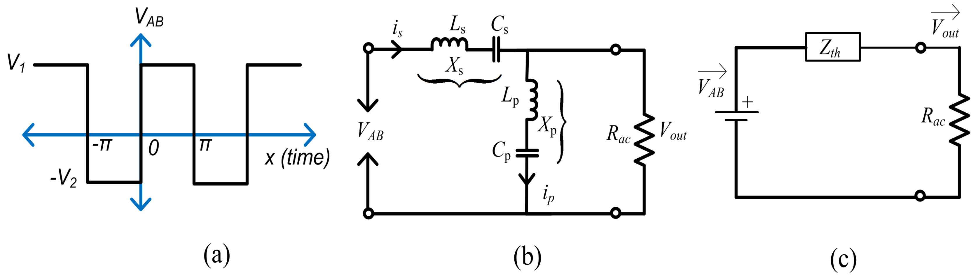
The proposed dual-input resonant converter is shown in Figure 1. In the converter and are the two voltage sources, , , and are the components of LCLC resonant tank. and are connected independently to the converter and transfer power to the load.
where and are the leakage inductances with reference to primary and tertiary windings of HF transformer respectively, where as and are the external physical inductors. Parallel branch of the tank circuit parameters and are placed on the tertiary side of HF transformer, and this avoids the HF transformer leakage inductance effect on circuit operation. In this connection, HF transformer Leakage inductances () are directly included in , and cannot be a troublesome or parasitic.
In this proposed converter, switches ( and ) operate in a complementary mode and then switching legs generate a square wave voltage across terminals AB. The generated square voltage acts as an excitation to the resonant tank circuit. Due to the filtering action of the series branch () of tank circuit, approximate sine wave current results in & . This current lags behind voltage (considering only the fundamental components of the square wave). Consequently, current is scaled and rectified by the HF transformer and bridge rectifier respectively. The rectified AC current is filtered by the output capacitors and outputs a DC voltage. Figure 2 shows the voltage and current waveforms of the resonant tank. The converter operation can be comprehended with help of steady state wave forms shown in Figure 2. Before time at t = switch and diodes & are conducting. At time gate voltage of is removed. In resonant converters, in lagging power factor mode of operation currents in the switches are lagging with respect to gate voltages. Therefore, at time t = , the existing non-zero value of switch current in is shifted to body diode . Whenever the current in decays to zero switch is turned-on with ZVS, as the body diode conducts till time . At time () rectifier diodes & enters into blocking mode. During the time interval < t < switch and rectifier diodes & are conducting, and this sequence of operations will repeat for every half cycle.
The input voltage () applied to the tank circuit which is symmetrical, only when the input voltages & are of the same value; otherwise, it leaves a DC component in . The DC component is filtered by the series resonant capacitor during unequal input voltages. In this way, the resonant tank circuit responds only to fundamental component (sinusoidal) of excitation voltage, even though voltage () is non-sinusoidal in nature. Hence, during un-equal dual input voltages, the HF transformer current is nearly symmetrical and, therefore, the saturation problem is minimised.
Fourier Series Expression for When the Input Voltages Are of Different Values
For simplification purposes, voltage is considered for 50% duty ratio and is shown in Figure 3a
Whose Fourier series expansion is
where & = 0 for n = 1, 2, … and
From the above analysis, the calculated DC component in is . This component is blocked by the capacitor for all the operating frequencies. During the converter operation, some portion of the resonant current flows through a parallel branch () and this parallel branch current varies based on its impedance; this current decreases as the frequency increases above the resonant value. Because of this characteristic nature, the output can be regulated at light loads with less variation in converter frequency compared to that in conventional resonant circuits.
3. Steady-State Analysis
In this section converter steady state behavior using AC circuit model is analyzed. The following are the assumptions in the converter steady state analysis: (i) high-frequency transformer is ideal; (ii) load on the converter is resistive; (iii) converter components (switches, capacitors and inductors) are ideal; (iv) voltage across terminals AB is considered as sinusoidal (fundamental component) for analysis. The equivalent circuit of the converter between the multi-input terminals AB is shown in Figure 3b. However, the tertiary winding parameters ( & ) are considered on the primary side of HF transformers for analysis purposes. The secondary side diode rectifier circuit including load is represented with AC resistance (), and is written as given in [10]. Where and , where . In the AC equivalent circuit of the converter, all the reactance’s are indicated by letter “X”, and its subscript represents a particular branch element. The switching frequency of the converter is rad/s) . Normalized switching frequency is , where (resonant frequency of tank circuit). In the converter steady state analysis normalised per unit (pu) values are indicated by extra subscript ’0’. In the normalization procedure of equations following base quantities are used, they are (resonant frequency of tank circuit (rad/s).
3.1. Series Branch Current
Current is derived by using (3) and from Figure 3b, as
Therefore per unit value of series branch current is calculated as
3.2. Per Unit Parallel Branch Current:
3.3. Voltage Across Series Branch:
3.4. Voltage Across Parallel Branch:
3.5. Converter Output Voltage Gain: M
Converter voltage gain is derived by using thevenin’s equivalent circuit of Ac equivalent circuit, which is shown in Figure 3c
where
3.6. The Peak Resonant Output Current: (Equal to Switch Peak Current)
3.7. Total KVA Rating of Tank Circuit Components per KW Output of Converter
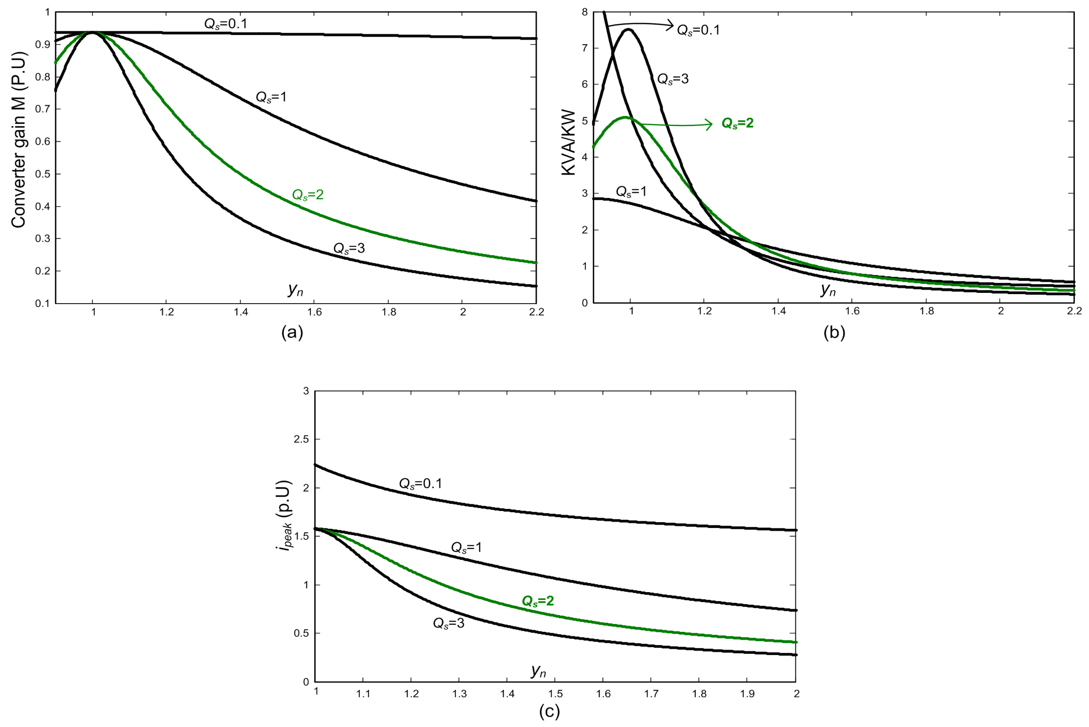
Satisfactory operation of the converter in terms of voltage regulation and ZVS turn-On for the defined operating power range depend on design parameters. Design parameters are selected using design curves and the design curves for LCLC resonant converter are shown in Figure 4. The following design curves are considered in the parameter selection.
- 1.
- Converter gain (M) versus : refer (11)
- 2.
- Peak resonant output current (switch peak current) versus : refer (14)
- 3.
- Total kVA/kW versus : refer (16)
These curves are plotted at lagging power factor mode at rated power condition for fixed ratios of ( = 0.1 & = 2) and at different quality factor () values. A converter design example by using design curves is explained in Section 5.
4. Control Scheme
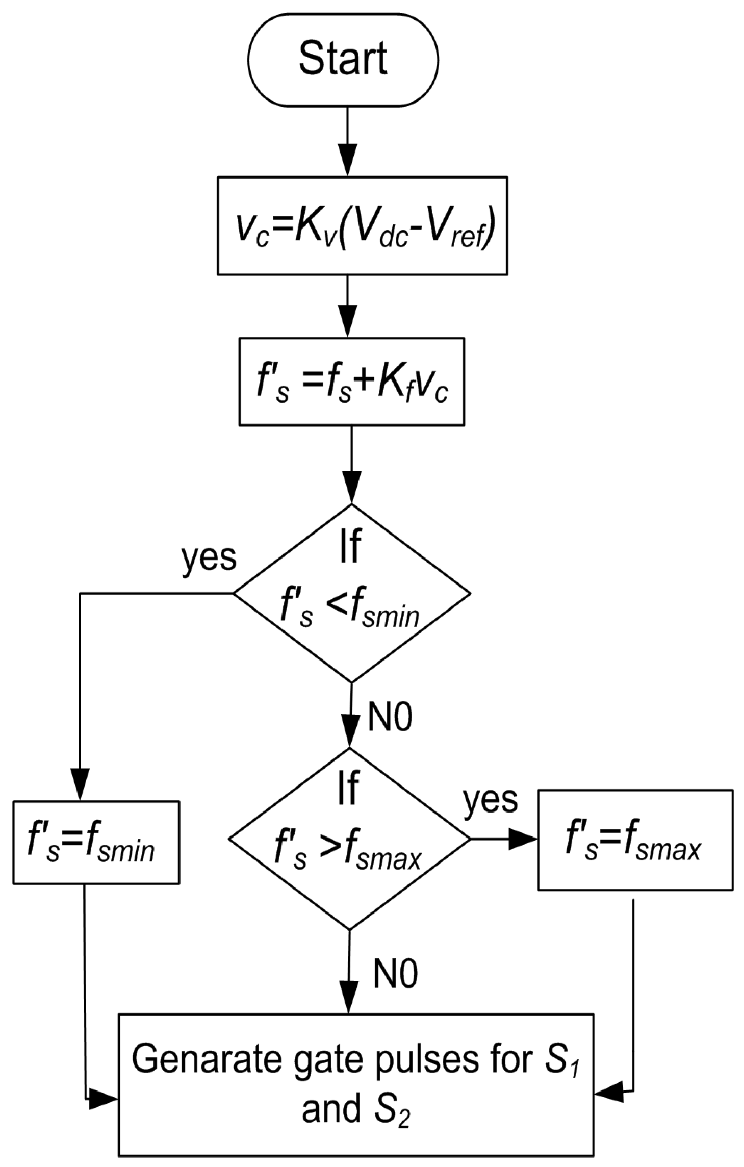
A closed-loop control scheme is required for regulating the output voltage on load variation. From (11), it is observed that converter voltage gain can be altered by varying the switching frequency, as and are the functions of . A decision algorithm is required for frequency modulation on load variation, in which a control voltage () is generated upon reference () comparison with load voltage ().
is the scaling factor
When load on the converter is reduced or input voltages increase, output voltage tends to be increased and regulate the output voltage; gain M must be reduced. This reduction in gain () is a function of change in output voltage and input voltage.
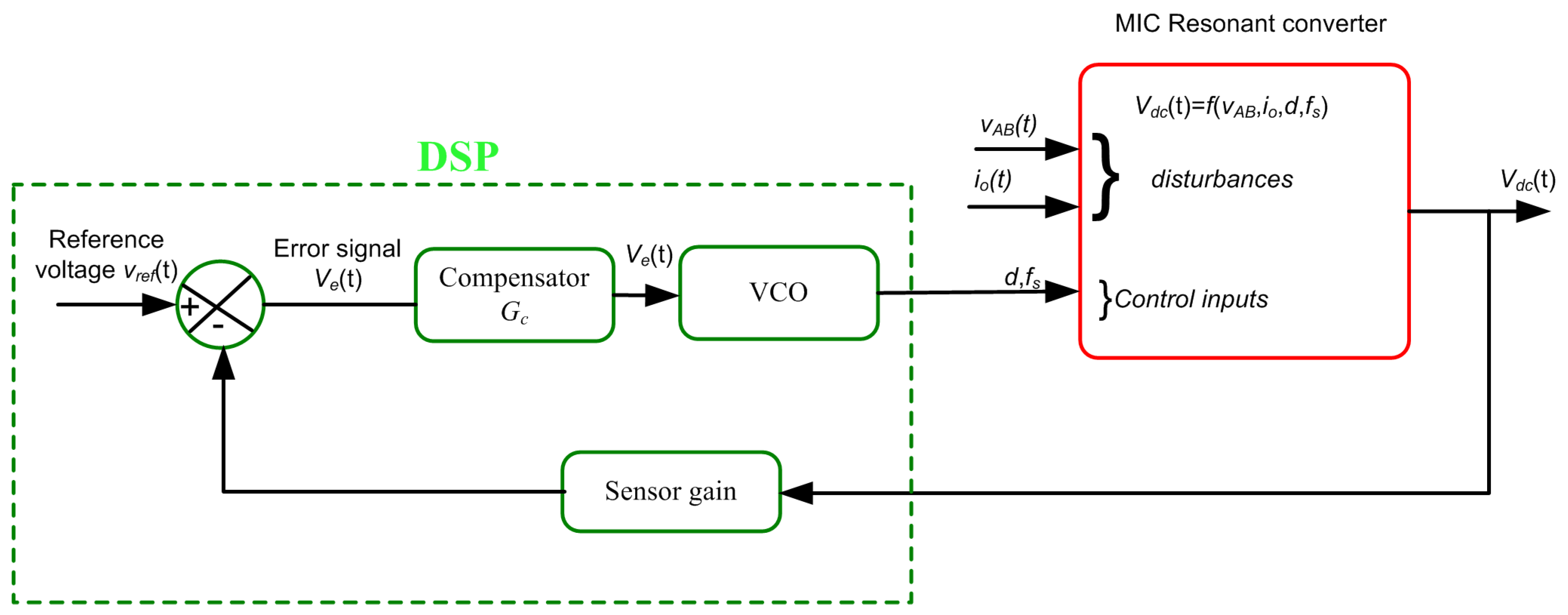
The new switching frequency is calculated from control voltage , where is the frequency constant and it is calculated for the required frequency variation between the lower and upper limits. A flow chart for the decision algorithm is shown in Figure 5. A voltage mode control closed loop block diagram for the proposed converter is shown in Figure 6. In this scheme, an error signal is generated by comparing output voltage with a reference value. The error is then processed through compensator . A control signal from the compensator is given to voltage control oscillator(VCO), and VCO generates gate pulses with the required frequency based on a decision algorithm. In this work, hardware is implemented for open loop configuration and the experimentation is conducted at different load conditions by changing the frequency manually.
5. Design Example
In this section converter design example is presented, design specifications are as follows Input
- voltage = 50 ± 10 V
- Output voltage = 380 V
- Power rating = 250 W
- Minimum switching frequency = 100 kHz
In order to design the resonant converter, several parameters such as light weight, lower switching losses, lower current rating of switching devices, higher efficiency, lower tank size and tight voltage regulation are considered for improvement of performance of the converter. However, several design curves are required to decide the optimum point of operation of these converters. In the design procedure, converter design is optimized for minimum transformer current , maximum efficiency and minimum KVA/KWA rating of the tank circuit components and minimum range of frequency control.
- (1)
- Converter gain (M) versus normalized switching frequency (): To keep the load voltage constant, the switching frequency variation is required. Converter gain (M) versus for a given ratio of and for different values of are plotted in Figure 4a. When the switching frequency is equal to the resonant frequency, converter gain (M) is the same for different values of . The lower the values of , the higher the converter gains; it is also seen from the design curves that output voltage can not be satisfactorily regulated for lower values of (like 0.1)
- (2)
- Total kVA/kW versus (): This is an important parameter for the optimum design of resonant converter. This parameter decides the tank size of resonant converter. The variation of total kilovolt-ampere per kilowatt (TkVA/kW) for given ratios of and and for different values of with normalized switching frequency () are plotted in Figure 4b. The total kVA rating increases as the value of increases. Also, the TkVA/kW-rating decreases with the switching frequency
- (3)
- Peak resonant output current () versus (): Inverter peak output current (same as the switch peak current) versus is plotted in Figure 4c for the given ratios of inductor and capacitor with different values of . It is observed that lower the value of , higher is the switch peak current also for higher values of (=3), inverter switch peak current is low.
Therefore, from the design curves, optimum value of is selected as 2. The normalized output voltage gain (M) for the optimum parameter values at ( = 1) is 0.9921 pu. Input voltage = 40 V ( < ), Output voltage = = 380 V, , where n is the turns ratio () = 0.0939. Even though, the converter is designed for maximum power (250 W) and minimum input voltage (40 V), use of frequency modulation ensures voltage regulation and ZVS i.e., satisfactory converter operation is possible up to 10% of rated load and at maximum input voltage (50 V).
By solving (20) and (22), it gives = 20 H and = 126 nF. Since = 0.1 and = 2, H and = 63 nF. The parallel branch components (inductor and capacitor ) are selected on tertiary winding of the HF transformer; therefore, they should transform to a tertiary side by using turns ratio (, therefore H and = 63 nF.
6. Results and Discussions
This section presents the hardware results for the proposed circuit, which are theoretically analyzed in the above sections.
Hardware Results
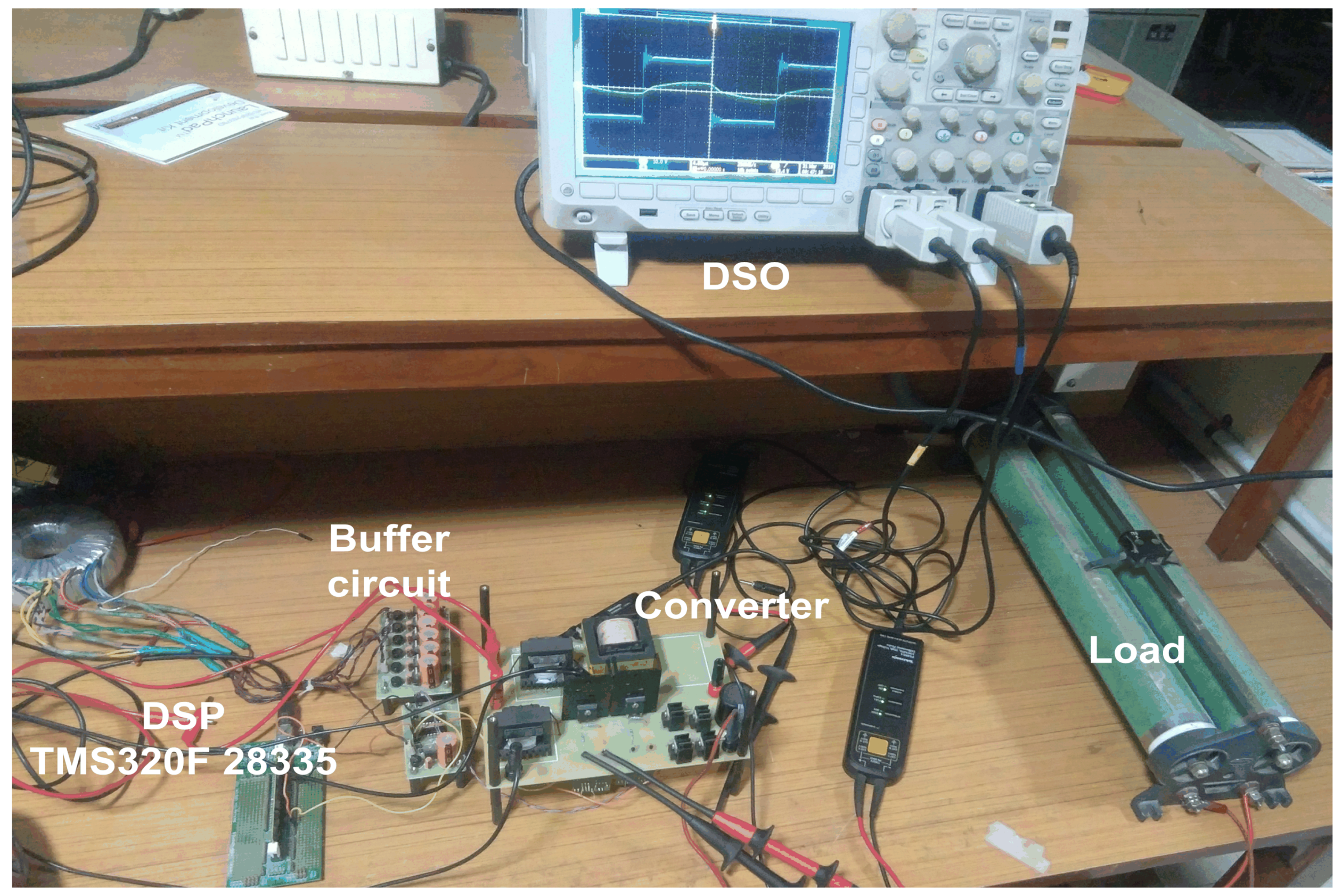
A 250 W experimental prototype is developed for the designed converter to verify the converter performance. Experimental setup is shown in Figure 7; its components and their specifications are shown in Table 1. The HF transformer and inductors in the prototype are prepared by using ferrite E core and litz wire, and the full bridge diode rectifier is made using BYC10D600 (NXP Semiconductors, Eindhoven, The Netherlands). Gate pulses for the switches are generated by using TMS320F28335 control card (Texas Instruments, Dallas, TX, USA) and gate driver circuits for MOSFET are designed by using MIC 4425 IC (Microchip Technology, Chandler, AZ, USA). The critical point operation of resonant converter is to maintain output voltage regulation at light load (10%), since at light loads, minimum value of tank circuit gain is required within the specified frequency range. Therefore, experimentation is conducted from full load to 10% of full load.
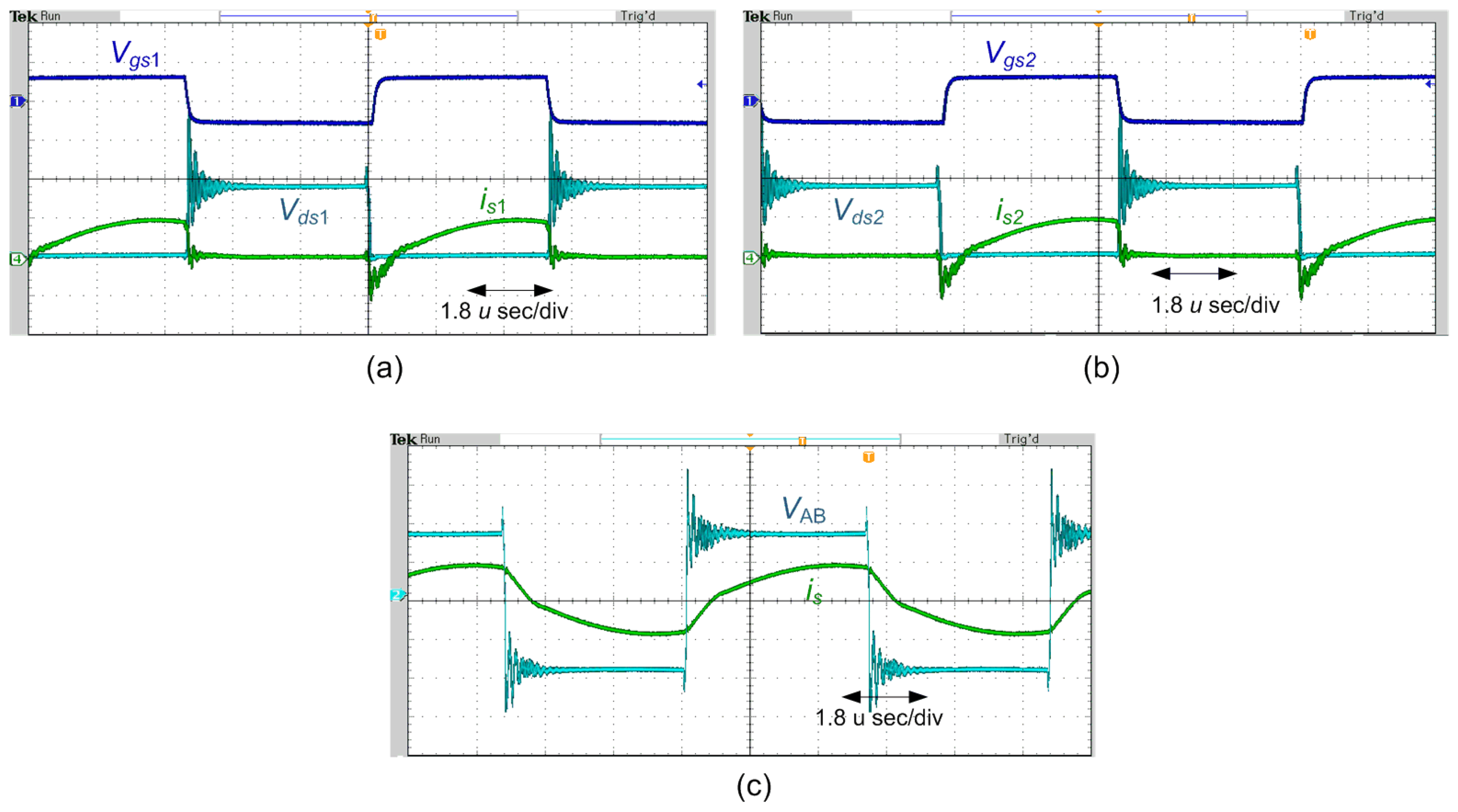
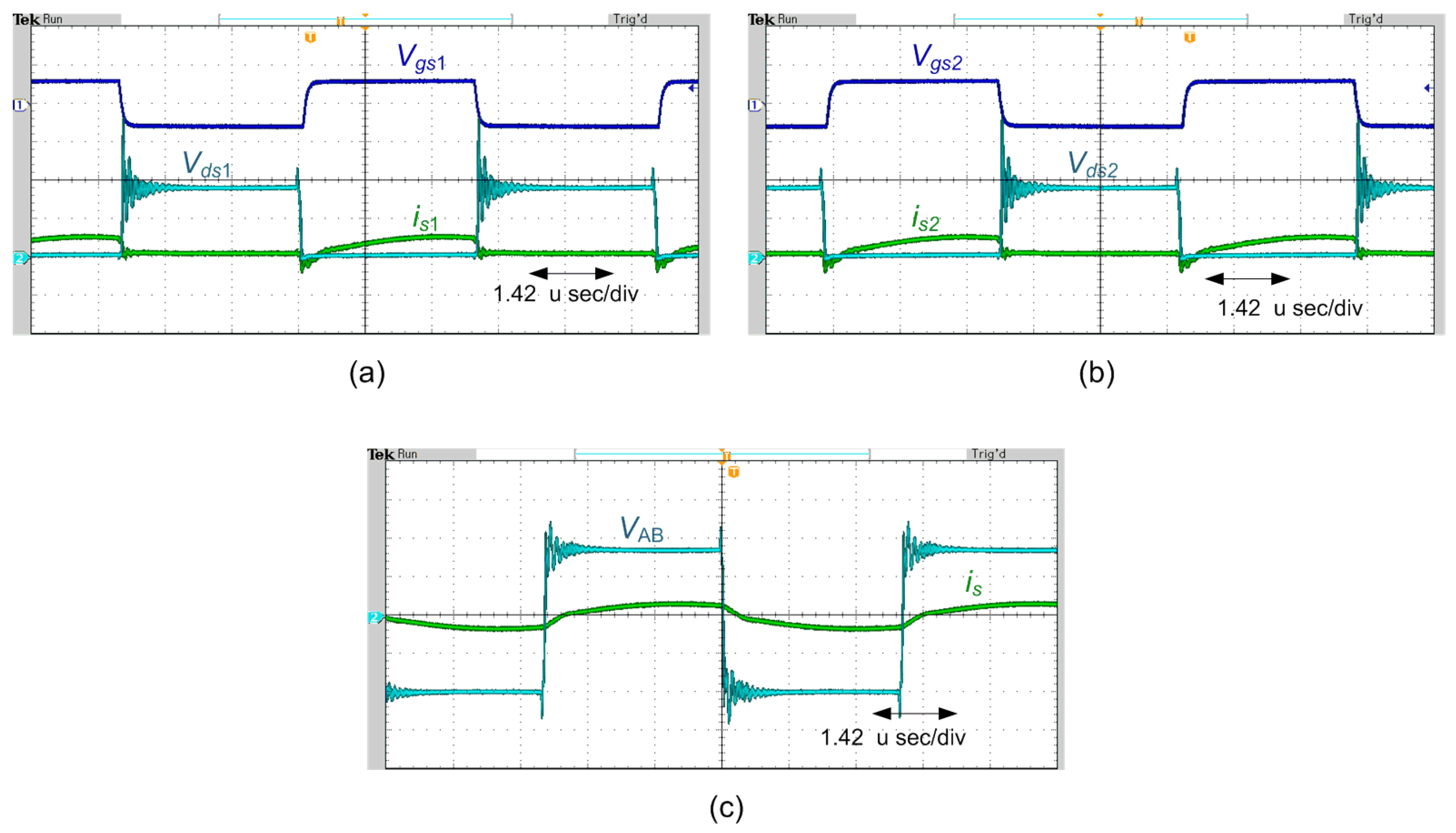
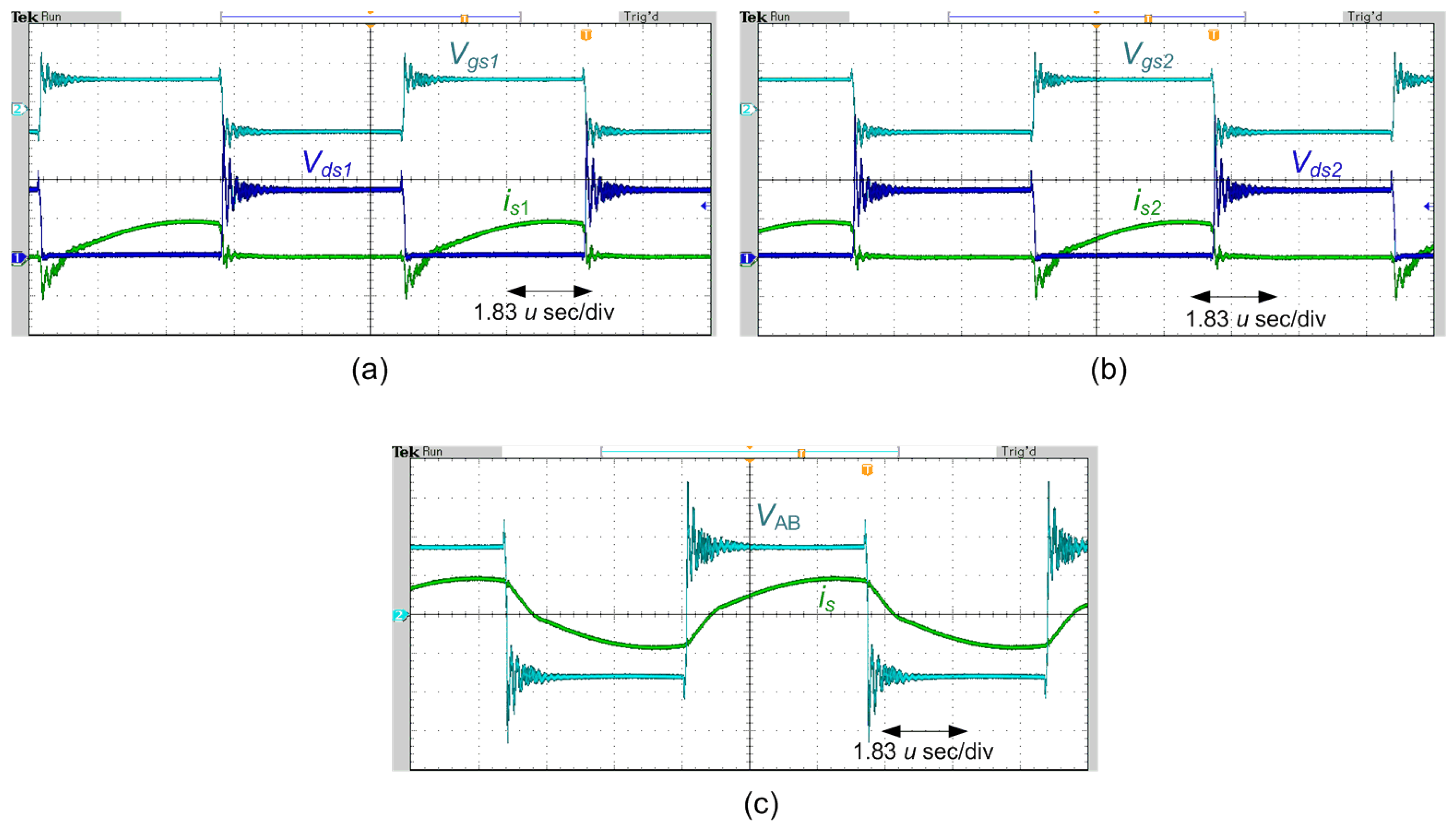
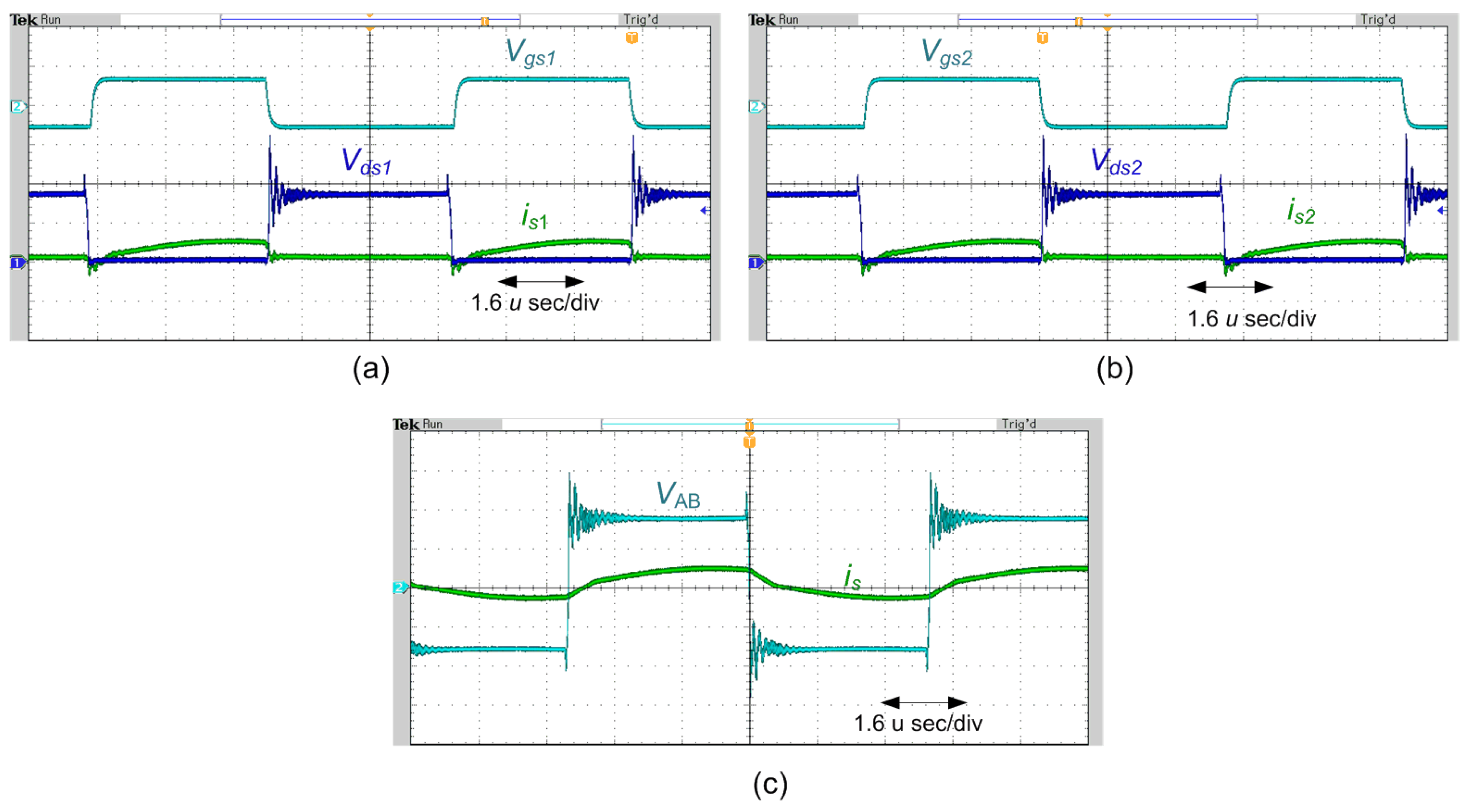
Figure 8 and Figure 9 show the experimental waveforms for = 42 V, = 48 V at peak load (250 W), and at 10% of peak load (25 W) respectively. Similarly, Figure 10 and Figure 11 show results for = 40 V, = 44 V at peak load (250 W), and at 10% of peak load (25 W) respectively. The operating frequency and duty ratio for the four operating conditions are given in Table 2. Figure 8a,b shows the switch voltage with switch current , and it confirms that switches and being operated with ZVS turn-on. Figure 8c depicts the inverter output voltage with respect to inverter output current . It is observed that current is nearly sinusoidal and lagging behind . Similarly Figure 9, Figure 10 and Figure 11 shows the experimental waveforms for remaining operating conditions. From the results, it is seen that ZVS in the switches & is well realised at rated load as well as at minimum load conditions.
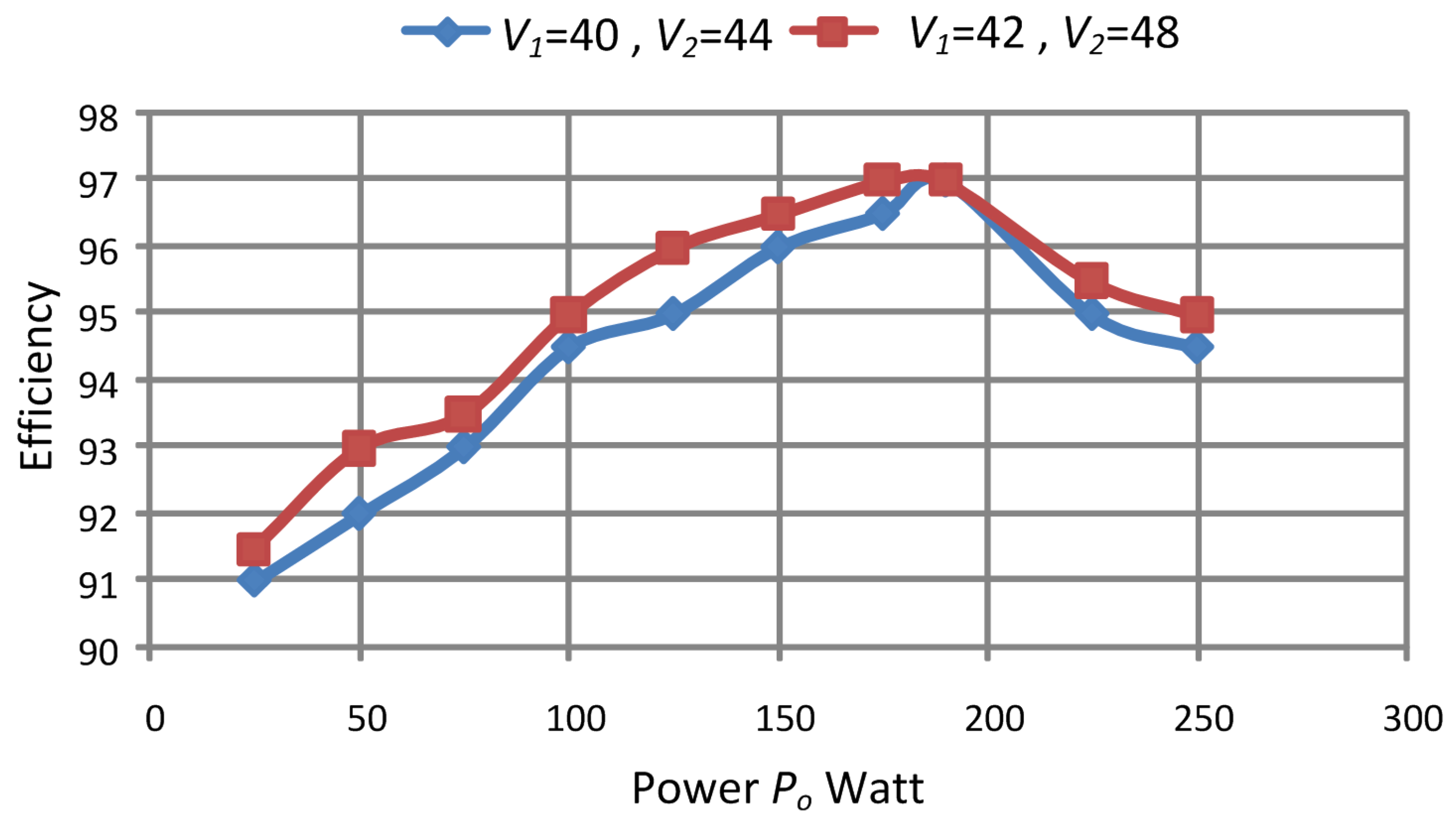
The measured efficiency curve for the hardware prototype at two different input voltage combinations with load variation is shown in Figure 12, which depicts that the overall system efficiency is above 90% and the highest efficiency is 97% at 75% of full-load conditions. It is observed that efficiency at full load is less when compared to 75% of full load, due to higher conduction losses in the primary side switches at full load. Similarly, at high input voltage combinations, efficiency is more due to lower currents in the switches and corresponding reduced conduction losses. Efficiency of the prototype can be further improved by using suitable components, surface mount devices with low ON-state resistance, optimized printed circuit board (PCB) design, etc.
7. Conclusions
In this paper, a highly efficient isolated resonant converter is proposed for dual-input single out-put applications. The proposed converter is simple in structure and also employs an effective technique to integrate two voltage sources with less number of switches. Converter performance is experimentally verified at varied load conditions in terms of ZVS and voltage regulation. Equal currents through switches are ensured in this converter even under unequal voltages at the input ports owing to reduction in transformer saturation-related issues. The maximum efficiency of the converter is 97% and is observed at 75% of full load. It is important to note that the driving signals of two switches are symmetrical i.e., duty cycles (D) of the two switches are equal. This helps to regulate the converter with minimum change in switching frequency.
Author Contributions
N.K.R. and M.R.R. developed the concept: H.M.S. and N.K.R. designed and performed the experiments: N.K.R. and M.R.R. wrote the paper; H.M.S. analyzed the data. These authors contributed equally to this work.
Funding
This research received no external funding.
Acknowledgments
Authors acknowledges the VNIT, Nagpur for providing infrastructure support.
Conflicts of Interest
The authors declare no conflict of interest.
References
- Reddi, N.K.; Ramteke, M.R.; Suryawanshi, H.M.; Kothapalli, K.; Gawande, S.P. An Isolated Multi-Input ZCS DC DC Front-End-Converter Based Multilevel Inverter for the Integration of Renewable Energy Sources. IEEE Trans. Ind. Appl. 2018, 54, 142–149. [Google Scholar] [CrossRef]
- Wu, T.F.; Chang, C.H.; Liu, Z.R.; Yu, T.H. Single-stage converters for photovoltaic powered lighting systems with MPPT and charging features. In Proceedings of the APEC ’98 Thirteenth Annual Applied Power Electronics Conference and Exposition, Anaheim, CA, USA, 15–19 Febuary 1998; Volume 2, pp. 1149–1155. [Google Scholar]
- Kolhe, M.; Joshi, J.C.; Kothari, D.P. Performance analysis of a directly coupled photovoltaic water-pumping system. IEEE Trans. Energy Convers. 2004, 19, 613–618. [Google Scholar] [CrossRef]
- Kjaer, S.B.; Pedersen, J.K.; Blaabjerg, F. A review of single-phase grid-connected inverters for photovoltaic modules. IEEE Trans. Ind. Appl. 2005, 41, 1292–1306. [Google Scholar] [CrossRef]
- Li, Y.; Ruan, X.; Yang, D.; Liu, F.; Tse, C.K. Synthesis of Multiple-Input DC/DC Converters. IEEE Trans. Power Electron. 2010, 25, 2372–2385. [Google Scholar] [CrossRef]
- Chen, Y.M.; Liu, Y.C.; Hung, S.C.; Cheng, C.S. Multi-Input Inverter for Grid-Connected Hybrid PV/Wind Power System. IEEE Trans. Power Electron. 2007, 22, 1070–1077. [Google Scholar] [CrossRef]
- Zeng, J.; Qiao, W.; Qu, L.; Jiao, Y. An Isolated Multiport DCDC Converter for Simultaneous Power Management of Multiple Different Renewable Energy Sources. IEEE J. Emerg. Sel. Top. Power Electron. 2014, 2, 70–78. [Google Scholar] [CrossRef]
- Dusmez, S.; Li, X.; Akin, B. A New Multiinput Three-Level DC/DC Converter. IEEE Trans. Power Electron. 2016, 31, 1230–1240. [Google Scholar] [CrossRef]
- Reddi, N.K.; Ramteke, M.R.; Suryawanshi, H.M. An isolated dual-input LCLC resonant converter for hybrid energy systems. In Proceedings of the IEEE International Conference on Industrial Technology (ICIT), Lyon, France, 20–22 Febuary 2018; pp. 629–633. [Google Scholar]
- Suryawanshi, H.M.; Tarnekar, S.G. Modified LCLC-type series resonant converter with improved performance. IEE Proc. Electr. Power Appl. 1996, 14, 354–360. [Google Scholar] [CrossRef]
- Dananjayan, P.; Chellamuthu, C. A new constant frequency zero voltage switching buck quasi-resonant converter. In Proceedings of the International Conference on Power Electronics, Drives and Energy Systems for Industrial Growth, New Delhi, India, 8–11 January 1996; Volume 1, pp. 176–182. [Google Scholar]
- Liu, K.H.; Lee, F.C. Zero-voltage switching technique in DC/DC converters. IEEE Trans. Power Electron. 1990, 5, 293–304. [Google Scholar] [CrossRef]
- Barbi, I.; da Silva, S.A.O. Sinusoidal line current rectification at unity power factor with boost quasi-resonant converters. In Proceedings of the Fifth Annual Proceedings on Applied Power Electronics Conference and Exposition, Los Angeles, CA, USA, 11–16 March 1990; pp. 553–562. [Google Scholar]
- Hua, G.; Lee, F.C. Soft-switching techniques in PWM converters. IEEE Trans. Ind. Electron. 1995, 42, 595–603. [Google Scholar] [CrossRef]
- Kheraluwala, M.H.; Steigerwald, R.L.; Gurumoorthy, R. A fast-response high power factor converter with a single power stage. In Proceedings of the Power Electronics Specialists Conference, Cambridge, MA, USA, 24–27 June 1991; pp. 769–779. [Google Scholar]
- Rajapandian, K.; Ramanarayanan, V.; Ramkumar, R. A 250 kHz/560 W phase modulated converter. In Proceedings of the International Conference on Power Electronics, Drives and Energy Systems for Industrial Growth, New Delhi, India, 8–11 January 1996; Volume 1, pp. 20–26. [Google Scholar]
Figure 1.
Proposed dual-input single output isolated resonant converter.

Figure 2.
Steady state waveforms.

Figure 3.
(a) Voltage across terminals AB; (b) Converter AC equivalent circuit; (c) Thevenin’s equivalent circuit.
Figure 3.
(a) Voltage across terminals AB; (b) Converter AC equivalent circuit; (c) Thevenin’s equivalent circuit.

Figure 4.
Design curves of LCLC resonant converter at = 0.1, = 2. (a) Normalized Converter Gain (M); (b) Total kVA/kW rating of tank circuit; (c) Normalized peak resonant output current .
Figure 4.
Design curves of LCLC resonant converter at = 0.1, = 2. (a) Normalized Converter Gain (M); (b) Total kVA/kW rating of tank circuit; (c) Normalized peak resonant output current .

Figure 5.
Flow chart for frequency modulation.

Figure 6.
Control diagram.

Figure 7.
Experimental setup.

Figure 8.
Experimental waveforms at , for 250 Watt load (a) (25 V/div), : (50 V/div), : (10 Amp/ div); (b) (25 V/div), : (50 V/div), : (10 Amp/ div); (c) : voltage across inverter (25 V/div), : resonant current (10 Amp/div).
Figure 8.
Experimental waveforms at , for 250 Watt load (a) (25 V/div), : (50 V/div), : (10 Amp/ div); (b) (25 V/div), : (50 V/div), : (10 Amp/ div); (c) : voltage across inverter (25 V/div), : resonant current (10 Amp/div).

Figure 9.
Experimental waveforms at , for 25 Watt load (a) : (25 V/div), : (50 V/div), : (2 Amp/ div); (b) : (25 V/div), : (50 V/div), : (2 Amp/ div); (c) : voltage across inverter (25 V/div), : resonant current (4 Amp/div).
Figure 9.
Experimental waveforms at , for 25 Watt load (a) : (25 V/div), : (50 V/div), : (2 Amp/ div); (b) : (25 V/div), : (50 V/div), : (2 Amp/ div); (c) : voltage across inverter (25 V/div), : resonant current (4 Amp/div).

Figure 10.
Experimental waveforms at , for 250 Watt load (a) : (25 V/div), : (50 V/div), : (10 Amp/ div); (b) :(25 V/div), : (50 V/div), :(10 Amp/div); (c) : voltage across inverter (25 V/div), : resonant current (10 Amp /div).
Figure 10.
Experimental waveforms at , for 250 Watt load (a) : (25 V/div), : (50 V/div), : (10 Amp/ div); (b) :(25 V/div), : (50 V/div), :(10 Amp/div); (c) : voltage across inverter (25 V/div), : resonant current (10 Amp /div).

Figure 11.
Experimental waveforms at , for 25 Watt load (a) : (25 V/div), : (50 V/div), : (2 Amp/div); (b) : (25 V/div), : (50 V/div), : (2 Amp/div); (c) : voltage across inverter (25 V/div), : resonant current (2 Amp V/div).
Figure 11.
Experimental waveforms at , for 25 Watt load (a) : (25 V/div), : (50 V/div), : (2 Amp/div); (b) : (25 V/div), : (50 V/div), : (2 Amp/div); (c) : voltage across inverter (25 V/div), : resonant current (2 Amp V/div).

Figure 12.
Measured efficiency curve.


Table 1.
Component Parameters of experimental Prototype.
| Components | Parameter |
|---|---|
| Primary side switches () | IRFP4227PbF: 200 V, 60 Amp, ( = 21 m) |
| HF Transformer | Total leakage inductance referred to primary H, |
| turns ratio = 1:10:1 (::) | |
| Hyper-fast diodes () | BYC10D600 |
| Resonant inductors | = 20 H, = 200 H Ferrite E core |
| Resonant capacitors | = 0.12 F, = 0.06 F (poly propylene film capacitors) |
| Output filter capacitor | = 100 F Electrolytic capacitor |
Table 2.
Case study results.
| (V) | (V) | Power (Watt) | Switching Frequency kHz | Duty Ratio D | Output Voltage |
|---|---|---|---|---|---|
| 42 | 48 | 250 | 108 | 0.47 | 380 |
| 42 | 48 | 25 | 135 | 0.47 | 380 |
| 40 | 44 | 250 | 105 | 0.47 | 380 |
| 40 | 44 | 25 | 120 | 0.47 | 380 |
© 2018 by the authors. Licensee MDPI, Basel, Switzerland. This article is an open access article distributed under the terms and conditions of the Creative Commons Attribution (CC BY) license (http://creativecommons.org/licenses/by/4.0/).
Share and Cite
MDPI and ACS Style
Reddi, N.K.; Ramteke, M.R.; Suryawanshi, H.M. Dual-Input Single-Output Isolated Resonant Converter with Zero Voltage Switching. Electronics 2018, 7, 96. https://doi.org/10.3390/electronics7060096
AMA Style
Reddi NK, Ramteke MR, Suryawanshi HM. Dual-Input Single-Output Isolated Resonant Converter with Zero Voltage Switching. Electronics. 2018; 7(6):96. https://doi.org/10.3390/electronics7060096
Chicago/Turabian StyleReddi, Naresh Kumar, Manojkumar Raju Ramteke, and Hiralal Murlidhar Suryawanshi. 2018. "Dual-Input Single-Output Isolated Resonant Converter with Zero Voltage Switching" Electronics 7, no. 6: 96. https://doi.org/10.3390/electronics7060096
Note that from the first issue of 2016, this journal uses article numbers instead of page numbers. See further details here.