Article

Analog Memristive Characteristics and Conditioned Reflex Study Based on Au/ZnO/ITO Devices

1
School of Physics & Optoelectric Engineering, GuangDong University of Technology, Guangzhou 510006, China
2
School of Electrical Engineering & Automation, JiangXi University of Science and Technology, Ganzhou 341000, China
*
Author to whom correspondence should be addressed.
Electronics 2018, 7(8), 141; https://doi.org/10.3390/electronics7080141
Submission received: 5 July 2018 / Revised: 28 July 2018 / Accepted: 1 August 2018 / Published: 8 August 2018
(This article belongs to the Special Issue Nanoelectronic Materials, Devices and Modeling)

Abstract

:
As the fourth basic electronic component, the application fields of the memristive devices are diverse. The digital resistive switching with sudden resistance change is suitable for the applications of information storage, while the analog memristive devices with gradual resistance change are required in the neural system simulation. In this paper, a transparent device of ZnO films deposited by the magnetron sputtering on indium tin oxides (ITO) glass was firstly prepared and found to show typical analog memristive switching behaviors, including an I–V curve that exhibits a ‘pinched hysteresis loops’ fingerprint. The conductive mechanism of the device was discussed, and the LTspice model was built to emulate the pinched hysteresis loops of the I–V curve. Based on the LTspice model and the Pavlov training circuit, a conditioned reflex experiment has been successfully completed both in the computer simulation and the physical analog circuits. The prepared device also displayed synapses-like characteristics, in which resistance decreased and gradually stabilized with time under the excitation of a series of voltage pulse signals.

Graphical Abstract

1. Introduction

Since the laboratory of Hewlett-Packard (HP) Development Company (Palo Alto, CA, USA) announced that the ‘missing’ circuit elements were found in 2008, memristive devices have attracted a great deal of attention worldwide as a potential element for future device applications, such as nonvolatile information storage and artificial neural network. Nonvolatile storage, characterized by abrupt resistance change and high ON/OFF ratio resistance states, is the basic feature of the digital memristor or resistive switching devices. However, the artificial neural network invariably needs analog memristive devices to implement synapses [1]. Smooth current–voltage curves with gradual change of the device resistance are the fingerprints of analog memristive devices, which are always known as analog resistive switching or analog memristor. There are considerable studies of analog memristor-based neural networks, because the gradual resistance provides a way to mimic synaptic strength and synaptic plasticity [2], and the advantages of a simple structure can be compared with pure software implementations [3,4]. Some studies have experimentally demonstrated memristor devices and showed that the hybrid system composed of complementary metal oxide semiconductor (CMOS) neurons and analog memristor synapses can support important synaptic functions, such as spike-timing-dependent plasticity [4,5]. Moreover, with the deepening of the memristor on the application of the integrated circuit, various mathematic and physical models related to memristors also have been a research hotspot in electronic engineering application. The first simulation program with integrated circuit emphasis (SPICE) model of memristor was put forward and built by Szmanda [6], and later on, McCreery successfully [7] modeled and simulated the characteristic curves of the HP memristor according to the data and modeling equation provided by the HP laboratory in 2004. Batas et al. [8] first introduced a behavior model of a memristive solid-state device for simulation with a SPICE compatible circuit. An original SPICE macro-model of the physically implemented memristor was presented by Rak [9], whose model offered a tool for electrical engineers to design and conduct new circuits with a memristor. Hu [10] recently presented a novel mathematical model for the TiO2 thin-film memristor device discovered by the HP laboratory, and the proposed model could be well applied to neural networks.
Although memristors have been widely studied in two aspects of material physics and modeling, the two researching fields were mostly in the state of independent development, and relatively little attention has been devoted to systematic research. Consequently, there are few reports that investigate the material characteristics and circuit model in a same work. In this paper, zinc oxide (ZnO) was chosen to fabricate the memeristive device because ZnO is an attractive memristive material [11,12] and semiconductor material with excellent magnetic, optical, and radiation-resisting advantages. Concretely, transparent substrate indium tin oxides (ITO) were used to construct an invisible ZnO/ITO/glass device, and the material properties were studied. Then a linear technology simulation program with integrated circuit emphasis (LTspice) model was built for the prepared device, and a Pavlov training circuit for neural network learning application was setup to verify the validity in the conditioned reflex.

2. Materials and Methods

ZnO thin films were prepared by magnetron sputtering on commercially available ITO glass, and the sputtering target was made of ZnO ceramic target with 99.99% purity. The films were deposited in a mixing atmosphere (argon:oxygen = 40:10, 0.5 Pa) and subsequently annealed in an oxygen atmosphere at 400 °C for 30 min. The gold (Au) top electrode layers were subsequently deposited on the ZnO thin film patterned by a shadow mask via Direct Current sputtering at room temperature. A source meter (Keithley 2400, Cleveland, OH, USA) was applied to the I–V measurement, and an oscilloscope (Tektronix, RSA306B, Beaverton, OR, USA) was used to record the physical waveform. The microstructure of the ZnO/ITO/glass structure was analyzed by a transmission electron microscope (TEM, FEI Tecnai G2F20, Hillsboro, OR, USA). The plan-view and cross-sectional TEM images are shown in Figure 1a and 1b, respectively. An interplanar distance of 0.263 nm was determined from Figure 1a, and this value matches the standard crystal face (002) of ZnO. An X-ray diffraction (XRD, Rigaku, Toyko, Japan) was also performed, and the resulting patterns shown in Figure S1 of the Supplementary Materials further prove the presence of wurtzite ZnO-related peaks corresponding to reflection (002) planes. About 120-nm-thick ZnO layers, which are clearly seen in Figure 1b, were believed to be well crystallized.

3. Results and Discussion

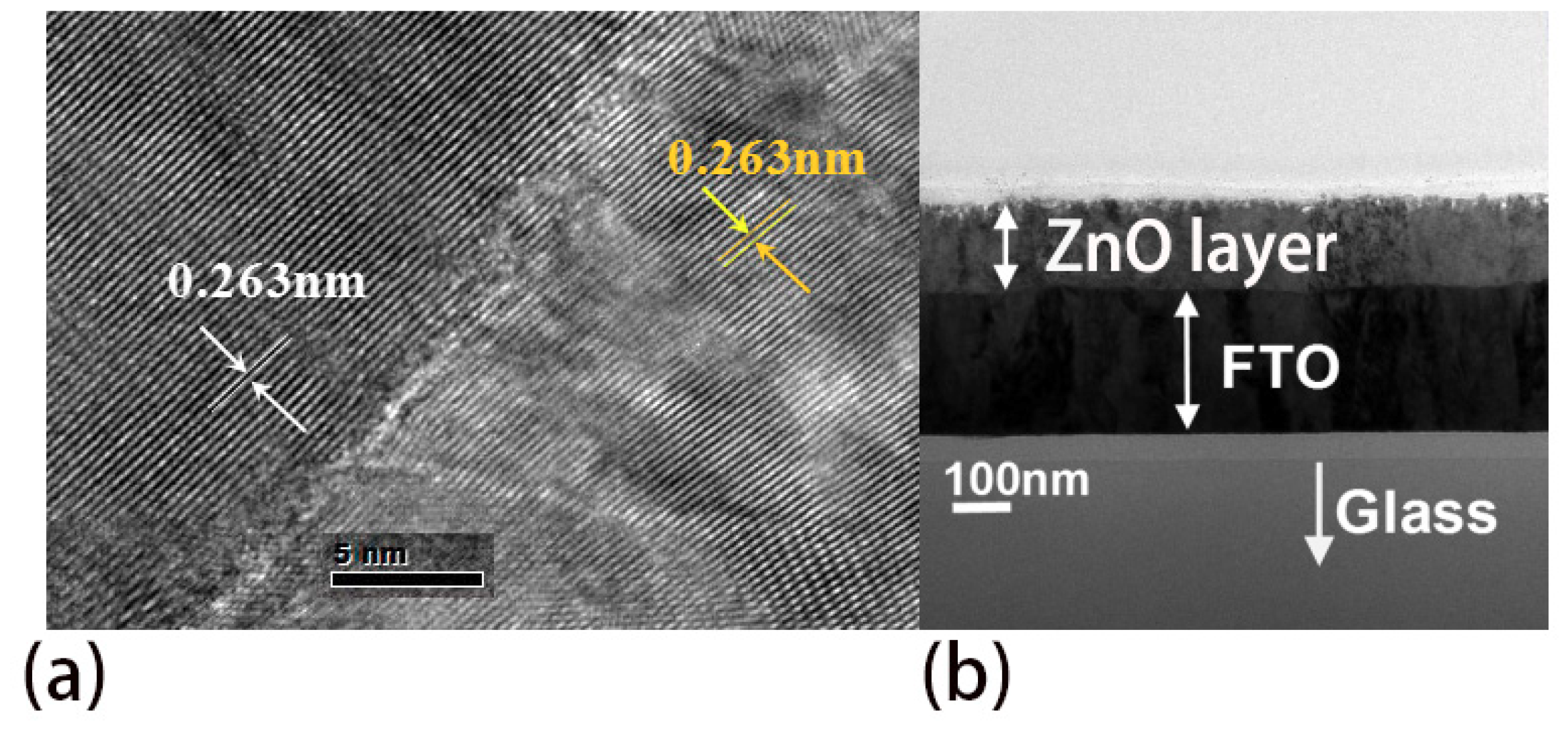
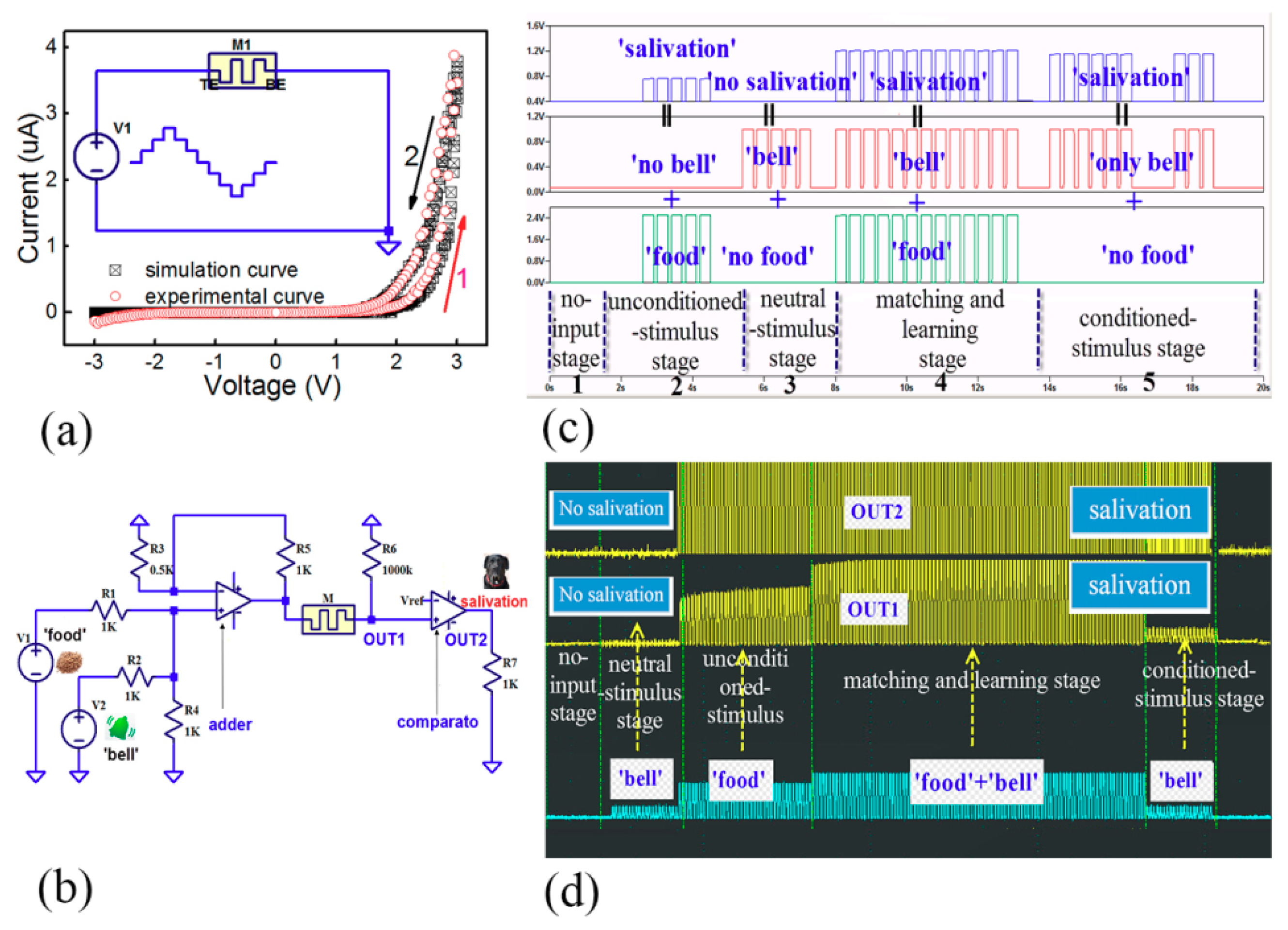
3.1. Confirmation of Memristor and I–V Characteristics

The I–V characteristics were examined by applying the output voltage of the source meter on ZnO/ITO, and positive bias was defined as the current flow from ZnO to ITO (the Au top electrode is positively biased, while the ITO bottom electrode was negatively biased). As shown in Figure 2a, the ZnO/ITO structure exhibited rectifying characteristics, and the reason behind it will be discussed below. In the positive bias region, a reproducible pinched hysteresis loop was recorded in Figure 2a for a single cycle at room temperature, as voltage was swept in the ‘1→2′ sequence with a rate of 0.1 V/step, and the time interval was 50 ms. In the reported literature about memristors, the Au/ZnO [11], SrTiO3:Nb/LaMnO3/Pt [13], and Ti/TiO2/Pt structures [14] also had the similar hysteresis loop I–V characteristic curve as that appeared in this work.
For a device to be a memristor, it should exhibit three characteristic fingerprints as follows: (1) the signature of pinched hysteresis loop in the voltage–current plane, (2) the hysteresis lobe area should decrease monotonically as the excitation frequency increases, and (3) the pinched hysteresis loop should shrink to a single-valued function when the frequency tends to infinity [15]. The prepared ZnO/ITO/glass, whose I–V curves are shown in Figure 2a, presents a pinched hysteresis loop similar to a Lissajous Figure as discussed in the literature [15]. To prove the frequency characteristic as the second fingerprint mentioned, we measured the I–V curves with different excitation frequencies, and the results in Figure 2b clearly demonstrate a shrinking loop as the frequency increases. This effect is consistent with fingerprints (2) and (3). In addition, the hysteresis direction of the first quadrant (the first half) is counterclockwise, which also coincides with the features of a typical memristor as proposed by Chua [16]. Hence, the experimental evidence suggests that the as-prepared ZnO/ITO/glass is a representative memristor device. As also clearly shown by the semilogarithmic current scale in the inset of Figure 2a, a set process was observed at about 1.3 V, while a reset process occurred at a voltage of about 2.3 V. This I–V curve can still be repeated after 100 cycles, indicating that the device has good reproducibility. We can find that the ratio of the highest resistance state (HRS) to the lowest resistance stage (LRS) is about 103. The current is only a few microamperes, which is two orders of magnitude smaller than most recently reported results [17]. In addition, no significant degradation of the device was observed when 6-month-old devices were tested, indicating good stability. The best reported structures of ZnO-based memristors having a good combination of low power, endurance, and retention performance so far is Ag/ZnO/Pt for electrochemical metallization memory devices [18]. To make a comparison, the major ZnO-based device parameters as a function of different metal electrodes are summarized in Table 1 [17].
In general, conducting mechanisms of memristive devices can be categorized into filamentary and homogeneous switching [19]. I–V curve of continuous resistance decreasing/increasing with gradual voltage sweep shown in Figure 2a, suggesting a homogeneous resistive switching or typical analog property instead of filamentary resistive switching or so-called digital resistive memristor. The main modes of carrier transport in memristive devices are ohmic and space charge limited (SCL) conduction and the I–V characteristics of SCL were defined by modified Child’s law [20] as shown in Equation (1):
I = ( 9 s ε 0 ε r μ n 8 d 3 ) θ V 2  
where s, ε, µn, and d are area, the dielectric constant, electron mobility, and the thickness of the device’s thin films, respectively. θ is the ratio of free carriers to trapped carriers. Figure 2c shows the log I–V curve for the positive sweep region. In the ‘0 V→3 V’ region, the curve is obviously divided into three stages (1, 2, and 3). It can be seen from the inset of Figure 2c that the I–V relation is linear under the application of a low electric field (0–1.2 V) as shown in stage 1. When the applied voltage reaches VSET (i.e., 1.3 V), the I–V curve is quadratic. When the voltage is increased to about 2.6 V, then the current rises rapidly, and the slope is six times that of stage 1. The low electric field should be defined as the Ohm zone, where the thermal electric conduction is dominated by an intrinsic carrier. When applied voltage reaches VSET, the I–V curve changes from Ohmic to SCL conduction, and the carrier transit time is equal to the Ohmic relaxation time [20]. In stage 3, because the injected excess carriers dominate the thermally generated carriers, it leads to a greater ratio of free carriers to trapped carriers, and the current behavior switches to the trap-free SCL conduction. In the ‘3 V→0 V’ region, the reason for the hysteresis is because the trapped carriers are not released completely with the reducing voltage [20].
The typical rectifying characteristics shown in the I–V curve of Figure 2a are due to the contact formed at the Au/ZnO/ITO structure interface. As we know, the work function of ITO is about WITO = 4.4 eV [21], the electron affinity of ZnO is EZnO ≈ 4.45 eV (ZnO is usually an N-type semiconductor) [22], and the work function of Au is WAu = 5.1 eV. Thus, ITO shows low barrier height when contacting ZnO, and ohmic contact of the ZnO/ITO interface can form easily. However, because WAu ≫ EZnO and Au was considered to be the shared material to construct the Schottky contact with the N-type ZnO, a rectifying effect could be formed between the interface of Au and ZnO. Once a rectifying contact is formed, the electrons in the ZnO films enter Au through the interface where the space-charge zone was constituted, and a built-in potential barrier that points from the ZnO surface to the top-electrode Au was constructed to stop the electrons from diffusing into the Au. Owing to impurity and defects caused in the process, the actual values of built-in potential are different, and the difference is reflected in the value of VSET. When the voltage applied on the top Au electrode is negatively biased, the built-in potential was enhanced with an external electric field, and the current value was almost zero.

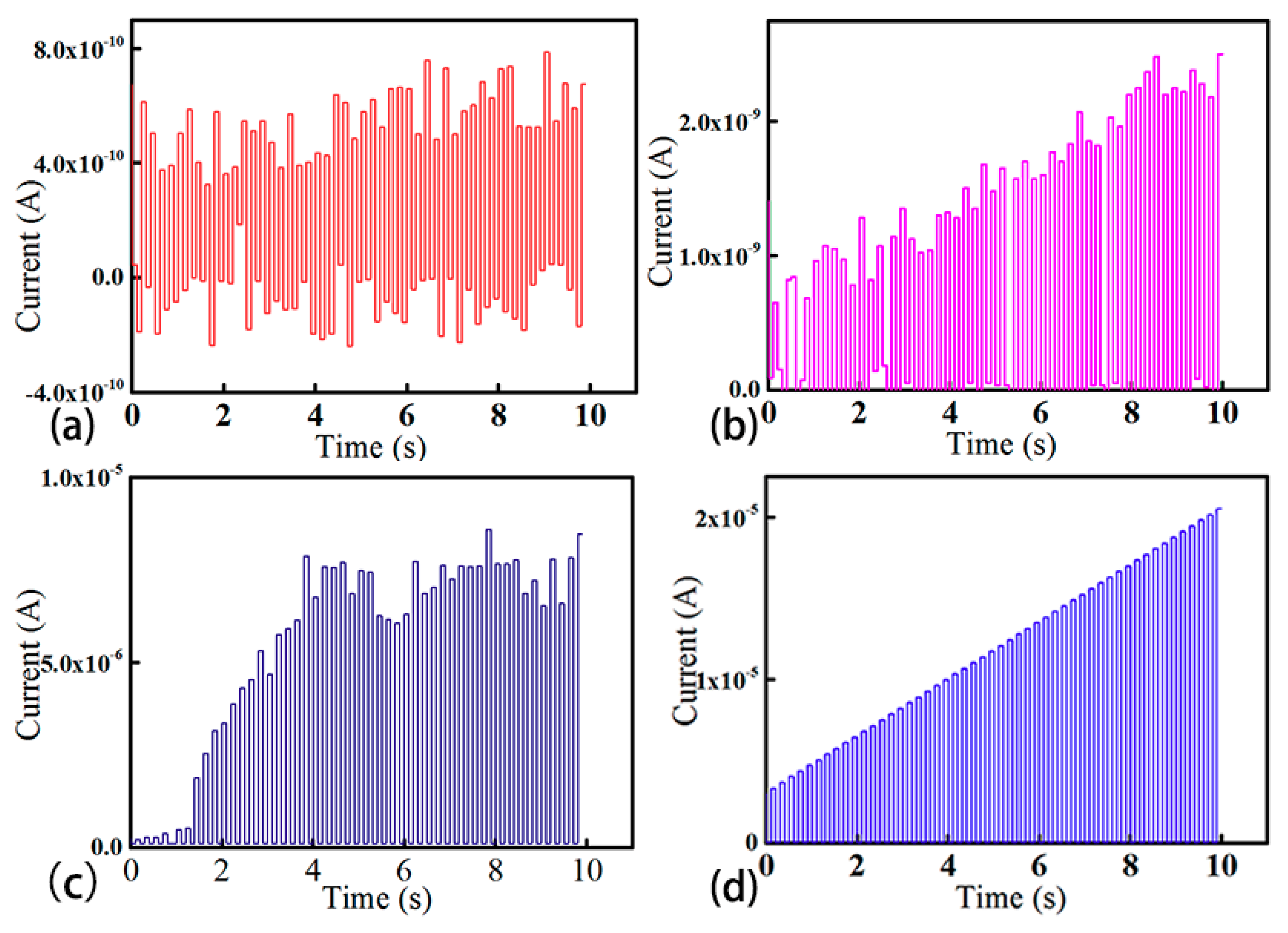
3.2. Memorizing Characteristics

To explore memorizing properties of the device in a physical circuit system, the same measurement configuration as described in Section 3.1 was used, and continuous voltage pulses (duty cycle is 1) with different amplitudes were applied to study the memristive characteristics of the device. Figure 3a shows the current–time (I–t) curve of the device undergoing 50 continuous voltage pulses with an amplitude of 1 V. Because the applied voltage did not exceed VSET voltage (1.3 V), the corresponding current was at 1010 A order, and this result exhibited an excellent endurance of HRS. Figure 3b shows the I–t curve under the application of 50 voltage pulses with an amplitude of 2 V. Because the voltage amplitude has exceeded the VSET value, the current value was larger than that under the application of 1 V pulse, and the resistance shows a decreasing trend with the continuous pulse application. Figure 3c shows the I–t curve under the application of 50 voltage pulses with an amplitude of 3 V. It is obvious that, in the applying process of the first several pulses, the device presents high impedance. However, with the further increasing of the number of pulses, the current rises to 10−6.A order rapidly, and the resistance dropped sharply. Figure 3d shows the I–t curve of the device under the continuous application of 100 voltage pulses with an amplitude of 4 V. The experimental results showed that, after the sample changed to LRS from HRS, the resistance did not keep in a stable LRS. Instead of dropping with the continuous application of pulses, this indicated that the device probably broke down.
As mentioned in the introduction, the analog memristive device was always considered to be the electronic component that is most similar to cerebral synapses [23]. In Figure 3c, when Vmax of the circular voltage exceeds the set voltage, the conductance of the device shows progressive increasing with the numbers of pulse and exhibits a saturation feature. This characteristic is similar to the function of synapses in neuromorphic engineering which means that the reinforcement and inhibition functions of synapses can be simulated through the device [24]. If voltage pulses imposed on the top electrode and bottom electrode of the device were regarded as pre-stimulus and post-stimulus of synapses, spike-timing-dependent-plasticity (STDP), as a crucial form of Hebbian learning, could be simulated through the device by programmable voltage pulse. A resistive switching of Ti/ZnO/Pt memristive devices was prepared and based on which STDP learning rule was implemented [25].

3.3. LTspice Models and Simulation

Common mathematical models of memristors include the HP model [26], the threshold model [27], and the matching model [28]. In particular, the matching model, proposed by Chris Yakopcic, has the characteristics of other two models and could accurately simulate multiple memristors (such as TiO2, Ge2Se3, etc.) by adjusting parameters. Moreover, the model has outstanding advantages in the memristor-based neural network simulation. Lai [29] further proposed the general thin-film memristor model based on the matching model. The above two matching models have a similar understructure, whose basic formula [30] is as follows in Equation (2):
I ( t ) = { a 1 ω ( t ) sinh ( b 1 V ( t ) )       If    V ( t ) 0 a 2 ω ( t ) sinh ( b 2 V ( t ) )      If    V ( t ) 0
where I(t) is the current through the memristor. V(t) is the voltage crossing the memristor. a i and b i are constants that are larger than zero, are respectively used to control the direction of current I(t), and indicate the effect of voltage V(t). ω is a variable that represents the internal states of the memristor as shown in Equation (3):
d ω d t = { c 1 sinh ( d 1 V ( t ) )        If    V ( t ) 0 c 2 sinh ( d 2 V ( t ) )       If   V ( t ) 0
where d ω / d t are directly proportional to the drifting velocity of charged particles (such as oxygen vacancies) in the memristor. c i and d i are constants that are larger than zero and are set according to the conductance of samples. In the actual physical process of the memristor, the drifting velocity of the particle and the applied electric field show a nonlinear relationship. In order to describe such a nonlinear relationship in mathematics, usually, a nonlinear window function [31,32] was appended on Equation (3). Among those proposed window functions, Prodromakis et al. presented a fine window function, as follows in Equation (4), which kept the continuity of the function and showed commendable ability in regulation:
f ( x ) = j ( 1 [ x 0.5 2 + 0.75 ] p )  
where j and x are the scalar parameter and current, respectively. p acts as any positive-real number and is employed to characterize the nonlinearities of the function. The nonlinearity is inversely proportional to the value of p: the smaller the p, higher the nonlinearity of the window function. Hence, Equation (3) can be transformed as Equation (5):
  d ω d t = { c 1 sinh ( d 1 V ( t ) ) f ( x ( t ) )        If    V ( t ) 0 c 2 sinh ( d 2 V ( t ) ) f ( x ( t ) )        If    V ( t ) 0
According to the above mathematical model and the I–V experimental data, the optimized parameters were obtained by carefully adjusting, and the LTspice code for the memristor is shown in Section S1 of the Supplementary Materials. With the LTspice code, a simulation I–V curve, which in line with the experimental results, is shown in Figure 4a, and we can find that VSET, VRESET, and the current order show good agreement with the experimental results. The simulation schematic is shown in the inset of Figure 4a, where M1 is the memristor and V1 is a step-wave voltage source with 0.05 V voltage-step and 50 ms time interval.

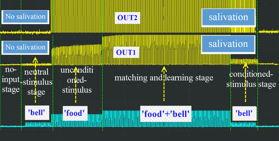
3.4. Conditioned Reflex Simulation and Circuit Experiments

In order to verify the potential significance of the memristor on the conditioned reflex, we employed the prepared ZnO/ITO/glass device to design a Pavlov training circuit [33,34] as shown in Figure 4b and then conducted a simulation and real physical experiments. In Pavlov’s experiments, food for the dog was used to activate an unconditioned stimulus (UCS) and the ring of a bell represents the neutral stimulus (NS). Once the food signal was received, Pavlov’s dog started to salivate. However, at first, the ring alone did not lead to any salivation by Pavlov’s dog. By feeding and ringing at the same time, Pavlov’s dog learned to associate the NS with the UCS. As a result, Pavlov’s dog salivated by even hearing the bell ring alone [34]. In the circuit of Figure 4b, V1 and V2 were used to generate voltage pulses for simulating food and bell signals, respectively. A comparator was used for signal shaping. The ‘OUT1’ and ‘OUT2’ in the circuit of Figure 4b represent ‘salivation’ before and after signal shaping.
Based on the LTspice mode and the designed Pavlov training circuit, a simulation results with five distinct stages, were shown in Figure 4c. In stage 1 (i.e., the no-input stage), there is no outputting signal, because the adder outputs a low level that induces the memristor M to stay in HRS, which limits OUT1 and OUT2, holding them in the low level. As shown in stage 2 (the UCS stage), when the voltage pulse, which represents the ‘food’ signal, holds for several periods (the amplitude is higher than V SET ), the adder will output high-level pulses, which leads the M to change from HRS to LRS, as demonstrated in Figure 3c. As a result, a pulse signal that represents the ‘salivation’ appears on both OUT1 and OUT2 of the Pavlov training circuit. If there is only one input of the ‘bell’ signal (the amplitude is lower than V SET ), as shown in stage 3, OUT2 also could not output a pulse signal, because the ‘bell’ voltage amplitude is too low to cause the M to go into LRS, resulting in OUT1 and OUT2 staying in the low-level state. After the 3-stage experiments stated above, in the event that both the ‘food’ and ‘bell’ signals are imputed at the same time, the adder performs a superposition operation on the two signals and outputs the resulting pulse, which leads the M to change from HRS to a retaining LRS. OUT1 and OUT2 hold in the high level as a consequence of the LRS of M. This can be called the matching and learning stage, as shown in stage 4 of Figure 4c. Afterwards, even if there is ‘no food’ input, the ‘dog’ can also secrete ‘salivation’ as the CS stage (stage 5) described, because the M is kept in LRS.
A set of input–output characteristics in Figure 4d were recorded for the Pavlov training circuit at room temperature for a ZnO/ITO/glass memristor as a synapse. Both the ‘bell’ and ‘food’ input signals were represented by voltage pulse signals with a frequency of 100 Hz and amplitude of 1.5 V. The commercial operational amplifiers LM358 (Motorola, Chicago, IL, USA) and TL072 (Texas Instruments Incorporated, Dallas, TX, USA) were used as adder and comparator, respectively. Observe that the output is exactly the same as the result of the simulation, which confirms that the application of the memristive device in a conditioned reflex has been achieved.

4. Conclusions

In this paper, we employed the magnetron sputtering deposition method to successfully fabricate a memristor with ITO/ZnO/glass structure. Our results show that such devices possess the typical analog memristive device characteristics. Based on a mathematical model, a LTspice circuit model was simulated successfully for the device, and a Pavlov training circuit using a memristor as synapses was designed to accomplish the physical process of matching and learning. In addition, because the current in the devices under 3 V turns out to be in the order of μA, the proposed ZnO-based memristor has great potential for commercial applications of artificial intelligence.

Supplementary Materials

The following are available at the following link: https://www.mdpi.com/2079-9292/7/8/141/s1, Figure S1: XRD pattern of ZnO/ITO/glass structure; Section S1: LTspice code of as prepared memristor.

Author Contributions

Conceptualization, T.C. and X.T.; Mathematical Model, J.R. and N.L.; and Circuit Design, L.Y.

Funding

This research was funded by “the National Natural Science Foundation of China 11574057”, “the Science Foundation of Department of Education of JiangXi Province [GJJ15331]”, “the Guangdong Provincial Natural Science Foundation of China [2016A030313718]” and “the Foundation of JXUST [NSFJ2015-K11]”.

Conflicts of Interest

The authors declare no conflict of interest.

References

  1. Lv, F.; Yang, R.; Guo, X. Analog and digital reset processes observed in Pt/CuO/Pt memristive devices. Solid State Ion. 2017, 303, 161–166. [Google Scholar] [CrossRef]
  2. Ravichandran, V.; Li, C.; Banagozar, A.; Yang, J.J.; Xia, Q.F. Artificial neural networks based on memristive devices. Sci. China Inform. Sci. 2018, 61, 1–14. [Google Scholar] [CrossRef]
  3. Pershin, Y.V.; Ventra, D.M. Practical approach to programmable analog circuits with memristors. IEEE Trans. Circuits Syst. I Reg. Pap. 2010, 57, 1857–1864. [Google Scholar] [CrossRef]
  4. Jo, S.H.; Chang, T.; Ebong, I.; Bhadviya, B.B.; Mazumder, P.; Lu, W. Nanoscale memristor device as synapse in neuromorphic systems. Nano Lett. 2010, 10, 1297–1301. [Google Scholar] [CrossRef] [PubMed]
  5. Kim, H.; Sah, M.P.; Yang, C.; Roska, T.; Chua, L.O. Neural synaptic weighting with a pulse-based memristor circuit. Trans. Circuits Syst. I Reg. Pap. 2012, 59, 148–158. [Google Scholar] [CrossRef]
  6. Ouyang, J.; Chu, C.W.; Szmanda, C.R.; Ma, L.; Yang, Y. Programmable polymer thin film and non-volatile memory device. Nat. Mater. 2004, 3, 918–922. [Google Scholar] [CrossRef] [PubMed]
  7. Wu, J.; Mccreery, R.L. Solid-state electrochemistry in molecule/TiO2 molecular heterojunctions as the basis of the TiO2 “memristor”. J. Electrochem. Soc. 2009, 156, 29–37. [Google Scholar] [CrossRef]
  8. Batas, D.; Fiedler, H. A memristor spice implementation and a new approach for magnetic flux controlled memristor modeling. IEEE Trans. Nanotechnol. 2011, 10, 250–255. [Google Scholar] [CrossRef]
  9. Rak, A.; Cserey, G. Macromodeling of the memristor in SPICE. IEEE Trans. Comput.-Aided Des. Integr. Circuits Syst. 2010, 29, 632–636. [Google Scholar] [CrossRef]
  10. Hu, X.; Feng, G.; Li, H.; Chen, Y.; Duan, S. An adjustable memristor model and its application in small-world neural networks. In Proceedings of the 2014 International Joint Conference on Neural Networks (IJCNN), Beijing, China, 6–11 July 2014. [Google Scholar]
  11. Sun, Y.; Yan, X.; Zheng, X.; Liu, Y.; Shen, Y.; Ding, Y.; Zhang, Y. Effect of carrier screening on ZnO-based resistive switching memory devices. Nano Res. 2017, 10, 77–86. [Google Scholar] [CrossRef]
  12. Murali, S.; Rajachidambaram, J.S.; Han, S.Y.; Chang, C.H.; Herman, G.S.; Conley, J.F.J. Resistive switching in zinc–tin-oxide. Solid State Electron. 2013, 79, 248–252. [Google Scholar] [CrossRef]
  13. Xu, Z.; Jin, K.; Gu, L.; Jin, Y.; Ge, C.; Wang, C.; Guo, H.; Lu, R.; Zhao, H.; Yang, G. Evidence for a crucial role played by oxygen vacancies in LaMnO3 resistive switching memories. Small. 2012, 8, 1279–1284. [Google Scholar] [CrossRef] [PubMed]
  14. Fullam, S.; Ray, N.J.; Karpov, E.G. Cyclic resistive switching effect in plasma electrolytically oxidized mesoporous Pt/TiO2 structures. Superlatt. Microstruct. 2015, 82, 378–383. [Google Scholar] [CrossRef]
  15. Adhikari, S.P.; Sah, M.P.; Kim, H.; Chua, L. Three fingerprints of memristor. Trans. Circuits Syst. I Reg. Pap. 2013, 60, 3008–3021. [Google Scholar] [CrossRef]
  16. Chua, L. Resistance switching memories are memristors. Appl. Phys. A 2011, 102, 765–781. [Google Scholar] [CrossRef]
  17. Simanjuntak, F.M.; Panda, D.; Wei, K.H.; Tseng, T.Y. Status and prospects of ZnO-based resistive switching memory devices. Nanoscale Res. Lett. 2016, 11, 368–385. [Google Scholar] [CrossRef] [PubMed]
  18. Huang, Y.; Shen, Z.; Wu, Y.; Wang, X.; Zhang, S.; Shi, X.; Zeng, H. Amorphous ZnO based resistive random access memory. RSC Adv. 2016, 6, 7867–7872. [Google Scholar] [CrossRef]
  19. Huang, C.H.; Huang, J.S.; Lai, C.C.; Huang, H.W.; Lin, S.J.; Chueh, Y.L. Manipulated transformation of filamentary and homogeneous resistive switching on ZnO thin film memristor with controllable multistate. ACS Appl. Mater. Interfaces 2013, 5, 6017–6023. [Google Scholar] [CrossRef] [PubMed]
  20. Shang, D.S.; Wang, Q.; Chen, L.D.; Dong, R.; Li, X.M.; Zhang, W.Q. Effect of carrier trapping on the hysteretic current-voltage characteristics in Ag/La0.7Ca0.3MnO3/Pt heterostructures. Phys. Rev. B 2006, 73, 245427. [Google Scholar] [CrossRef]
  21. Nüesch, F.; Forsythe, E.W.; Le, Q.T.; Gao, Y.; Rothber, L.J. Importance of indium tin oxide surface acido basicity for charge injection into organic materials based light emitting diodes. J. Appl. Phys. 2000, 87, 7973–7980. [Google Scholar]
  22. Fang, Y.J.; Sha, J.; Wang, Z.L.; Wan, Y.T.; Xia, W.W.; Wang, Y.W. Behind the change of the photoluminescence property of metal-coated ZnO nanowire arrays. Appl. Phys. Lett. 2011, 98, 033103. [Google Scholar] [CrossRef]
  23. Ielmini, D. Brain-inspired computing with resistive switching memory (RRAM): Devices, synapses and neural networks. Microelectron. Eng. 2018, 190, 44–53. [Google Scholar] [CrossRef] [Green Version]
  24. Chang, T.; Jo, S.H.; Kim, K.H.; Sheridan, P.; Gaba, S.; Lu, W. Synaptic behaviors and modeling of a metal oxide memristive device. Appl. Phys. A 2011, 102, 857–863. [Google Scholar] [CrossRef]
  25. Pan, R.; Li, J.; Zhuge, F.; Zhu, L.; Liang, L.; Zhang, H.; Gao, J.; Cao, H.; Fu, B.; Li, K. Synaptic devices based on purely electronic memristors. Appl. Phys. Lett. 2016, 108, 382001. [Google Scholar] [CrossRef]
  26. Biolek, Z.; Biolek, D.; Biolkova, V. SPICE model of memristor with nonlinear dopant drift. Radioengeering 2009, 18, 210–214. [Google Scholar]
  27. Pershin, Y.V.; Ventra, M.D. Experimental demonstration of associative memory with memristive neural networks. Neural Netw. 2010, 23, 881–886. [Google Scholar] [CrossRef] [PubMed] [Green Version]
  28. Yakopcic, C.; Taha, T.M. Subramanyam, G.; Pino, R.E.; Rogers, S. A memristor device model. IEEE Electron Device Lett. 2011, 32, 1436–1438. [Google Scholar] [CrossRef]
  29. Laiho, M.; Lehtonen, E.; Russel, A.; Dudek, P. Memristive synapses are becoming reality. Neuromorphic Eng. 2010. [Google Scholar] [CrossRef]
  30. Lehtonen, E.; Poikonen, J.; Laiho, M.; Wei, L. Time-dependency of the threshold voltage in memristive devices. IEEE Int. Symp. Circuits Syst. 2011, 19, 2245–2248. [Google Scholar]
  31. Yu, J.; Mu, X.; Xi, X.; Wang, S. A memristor model with piecewise window function. Radioengineering 2013, 22, 969–974. [Google Scholar]
  32. Prodromakis, T.; Peh, B.; Papavassiliou, C.; Toumazou, C. A versatile memristor model with nonlinear dopant kinetics. IEEE Trans. Electron Devices 2011, 58, 3099–3105. [Google Scholar] [CrossRef]
  33. Wang, F.Z.; Helian, N.; Wu, S.; Yang, X.; Guo, Y.K.; Lim, G.; Rashid, M.M. Delayed switching applied to memristor neural networks. J. Appl. Phys. 2012, 111, 07E317. [Google Scholar] [CrossRef]
  34. Ziegler, M.; Soni, R.; Patelczyk, T.; Ignatov, M.; Bartsch, T.; Meuffels, P.; Kohlstedt, H. An electronic version of pavlov’s dog. Adv. Funct. Mater. 2012, 22, 2744–2749. [Google Scholar] [CrossRef]
Figure 1. Transmission electron microscope (TEM) images of the zinc oxide (ZnO)/indium tin oxide (ITO)/glass structure (a) plan-view and (b) cross-sectional image.
Electronics 07 00141 g001
Figure 2. I–V characteristic curve (a) I–V curve at room temperature; (b) frequency-independent I–V curve; and (c) logI–logV characteristics curve.
Electronics 07 00141 g002
Figure 3. I–t curve of the device undergoing 50 voltage pulses with (a) an amplitude of 1 V; (b) an amplitude of 2 V; (c) an amplitude of 3 V; and (d) an amplitude of 4 V (100 pulses).
Electronics 07 00141 g003
Figure 4. Simulation and experimental results (a) Simulation results of the device using the LTspice model; (b) Pavlov training circuit; (c) Resulting simulation of Pavlov training circuit; (d) Physical experiment results. M1 is the memristor and V1 is a step-wave voltage source with 0.05 V voltage-step and 50 ms time interval.
Electronics 07 00141 g004
Table 1. ZnO-based resistive random access memory fabricated with various metal electrodes.
NoStructureCurrentEnduranceRoff/RonRetention
1Pt/ZnO/Pt30 mA100103–104not available
2Ru/ZnO/Pt10 mA20061104
3Ag/ZnO/Pt10 mA40100not available
4Cu/ZnO/ITOnot available300>20not available

