Article

Identifying Near-Perfect Tunneling in Discrete Metamaterial Loaded Waveguides

by
Kimberley W. Eccleston
* and
Ian G. Platt
Lincoln Agritech Ltd., Canterbury 7640, New Zealand
*
Author to whom correspondence should be addressed.
Electronics 2019, 8(1), 84; https://doi.org/10.3390/electronics8010084
Submission received: 25 October 2018 / Revised: 20 December 2018 / Accepted: 3 January 2019 / Published: 11 January 2019
(This article belongs to the Special Issue Engineering Metamaterials)

Abstract

:
Mu-negative and epsilon-negative loaded waveguides taken on their own are nominally cut-off. In ideal circumstances, and when paired in the correct proportions, tunneling will occur. However, due to losses and constraints imposed by finite-sized constituent elements, the ability to experimentally demonstrate tunneling may be hindered. A tunnel identification method has been developed and demonstrated to reveal tunneling behavior that is otherwise obscured. Using ABCD (voltage-current transmission) matrix formulation, the S-parameters of the mu-negative/epsilon-negative loaded waveguide junction is combined with S-parameters of an epsilon-negative loaded waveguide. The method yields symmetric scattering matrices, which allows the effect of losses to be removed to provide yet clearer identification of tunneling.

1. Introduction

The purpose of this work is to identify tunneling across an experimental microwave metamaterial heterojunction that may be obscured due to losses and constraints imposed by finite-sized constituent elements in real microwave metamaterials.
Microwave metamaterials exhibit unusual electromagnetic properties (such as negative permittivity and negative permeability) which yield a range of unusual phenomena. One such phenomenon is the tunneling of electromagnetic waves through epsilon-near-zero (ENZ) metamaterial [1,2,3,4,5], epsilon-negative (ENG) metamaterial (or empty waveguides operated at cut-off) paired with mu-negative (MNG) metamaterial [6,7,8,9,10,11,12,13,14,15], and cut-off waveguides either filled [16,17], or lined [18,19], with metamaterials. In this work, we are specifically interested in tunneling in a microwave waveguide filled by a ENG/MNG metamaterial heterojunction where the waveguide is cut-off when loaded by either the ENG or MNG metamaterial on its own [7,14].
ENG behavior can be obtained at microwave frequencies using an empty cut-off waveguide [7,14] or by loading the waveguide with an array of thin wires [20,21]. MNG behavior can be obtained at microwave frequencies by loading the waveguide with an array of split-ring resonators (SRRs) [7,14,20,22]. In both cases, lumped elements can also be used [8,9,10,13]. Practical microwave metamaterials are constructed from a discrete number of finite-sized elements. Therefore, in a practical experiment, it may not be possible to satisfy the length requirement (or attenuation condition) for perfect tunneling [6,7]. Hence, it is the purpose of this work to develop a method to identify tunneling behavior in discrete microwave ENG/MNG metamaterial junctions.
Whether using loaded waveguides or transmission lines, resistive losses impact on the ability to demonstrate tunneling [6,15]. Therefore, an additional purpose of this work is to isolate losses from experimental results to further reveal tunneling.

2. Theoretical Background

In this work we confine ourselves to time-harmonic electromagnetic waves. At a given angular frequency ω, each field component of an electromagnetic wave travelling in the positive z direction will contain the factor exp ( j ω t γ z ) where γ is the propagation constant and j = 1 . In general γ is complex valued and related to real valued attenuation and phase constants, α and β respectively, taking the form γ = α + j β . For passive media, the amplitude of the field components will either decay or remain constant with z and this means α is always greater than or equal zero. For the rest of this work we will drop explicit reference to the factor exp ( j ω t γ z ) and describe such quantities using phasor notation. Within the waveguide, we confine ourselves to transverse-electric (TE) wave propagation and consider the lowest order mode being the TE10 mode [23] since this simplifies the procedure to demonstrate tunneling.
Figure 1 shows a diagram of an idealized waveguide tunneling configuration which comprises four sections: Section 1 and Section 4 air-filled, and Section 2 and Section 3 being filled by μ-negative (MNG) and ε-negative (ENG) metamaterials respectively. For the moment, it will be assumed that the MNG and ENG metamaterials are continuous, lossless and isotropic. The waveguide cross-section is identical along the structure so the only discontinuity is a change of material along the longitudinal axis (z).
At a frequency above the TE10 mode cut-off frequency of Section 1 and Section 4, Section 1 and Section 4 will support propagation. On the other hand, Section 2 and Section 3 on their own, because their permittivity and permeability are opposite signed, will be cut-off (see Appendix A). It can be shown (see Appendix B) perfect transmission from port 1 to port 2 (zero insertion loss and zero reflection coefficient) occurs when [6,7]:
α E N G l E N G = α M N G l M N G
and:
Z E N G = Z M N G
where lMNG and lENG are the lengths of the MNG and ENG loaded waveguides respectively, and ZMNG and ZENG are the TE10 mode wave-impedances of the MNG and ENG metamaterials respectively. We denote (1) and (2) the attenuation and impedance tunneling conditions respectively.
As only evanescent modes can be excited in waveguides filled with lossless isotropic MNG and ENG metamaterials, ZMNG and ZENG will be purely imaginary with Im ( Z M N G ) < 0 and Im ( Z E N G ) > 0 (see Appendix A). Provided ZMNG and ZENG are of similar magnitude, the impedance tunneling condition can be satisfied at some frequency. On the other hand, the attenuation constant is always positive valued and this requires a certain length ratio to satisfy the attenuation tunneling condition. Similar conclusions are obtained for waveguides filled with certain continuous lossless anisotropic MNG and ENG metamaterials (see Appendix C) [7].
The single ENG/MNG heterojunction contained within the waveguide of Figure 1 represents the minimum configuration for tunneling. A five section waveguide tunneling structure may be realized as shown in Figure 2 where the length of Section 3 (ENG) is 2lENG. The tunneling conditions of Figure 2 are the same as Figure 1, and hence equations (1) and (2) apply to Figure 2. It is the structure of Figure 2 which forms the theoretical basis for the experimental tunneling identification. This structure is symmetrical which is useful when dealing with losses.

3. Tunneling in Practical Microwave Metamaterials

Practical microwave metamaterials employing split-ring resonators (SRRs) and thin wires to obtain MNG and ENG behavior respectively, are crystalline (periodic) structures with lattice constants of the order of millimeter [7,14,16,17,20,24,25]. So whilst significantly smaller than the guide wavelength, thereby approximating the continuous medium, the dimensions of practical metamaterial elements are never-the-less finite and means that material lengths take discrete values. It is unlikely that the attenuation tunneling condition is satisfied at the same frequency as the impedance tunneling condition when the ENG and MNG lengths are restricted to discrete values.
For example, for ENG and MNG metamaterials based upon the negative-refractive-index (NRI) metamaterials described by Eccleston & Platt [24], the length of the MNG metamaterial would be integer multiples of 5 mm and the ENG metamaterial takes lengths in integer increments of 20 mm. The significant difference in lattice constants arises from the need to achieve useful permittivity values within the low gigahertz range using an entirely printed structure [24]. As will be demonstrated in Section 5, perfect tunneling in such materials is obtained at 2.73 GHz when lMNG = 25 mm and lENG = 8.8 mm, which is incompatible with these lattice constraints of the materials. At higher frequencies, the lattice constant for ENG could be comparable to that of the MNG [25].
On the other hand, this problem does not arise when one of the metamaterials is continuous. For example, Baena et al. [7] use a SRR waveguide and an empty cut-off waveguide for MNG and ENG behavior respectively; lMNG and lENG are discrete and continuous respectively.

4. Tunnel Identification Principle

The procedure that will be described is aimed at identifying tunneling in a MNG/ENG junction constructed entirely from discrete metamaterials. Two sets of microwave scattering parameters [23] is required: (i) ENG/MNG filled waveguide junction, and (ii) ENG filled waveguide of known length. The former structure will be denoted the device-under-test (DUT) and contains the MNG/ENG heterojunction required for tunneling.
It will be assumed that MNG behavior is obtained over a narrow bandwidth using an array of split-ring resonators (SRRs), and ENG behavior is obtained over a significantly wider bandwidth using an array of strips. The term strip is used rather than wire to acknowledge implementation in printed-circuit-board (PCB) or similar technology [24,25].
The block diagram describing tunneling identification is shown in Figure 3a. The DUT and reversed DUT blocks represent the direct measurements of the DUT, whilst the middle section, of length lStrip2, is described by a transmission line model. The propagation constant and wave-impedance of the transmission line model are extracted from measurements of the strip loaded (ENG) waveguide. The length lStrip2 of the middle section of Figure 3a is in general different to the length of the measured strip loaded waveguide.
The cascade of Figure 3a is equivalent to the block diagram shown in Figure 3b. Comparing Figure 3b with Figure 2, then applying (1) and (2) to Figure 3b, it can be shown for lossless media, perfect tunneling occurs when:
2 α S R R l S R R = α S t r i p ( 2 l S t r i p 1 + l S t r i p 2 )
and
Z S R R = Z S t r i p
The ability to apply Figure 3a and its equivalent Figure 3b assumes only the dominant mode exists at the ports of each waveguide section depicted in Figure 3a, and that the strip loaded waveguide behaves as a homogenously filled waveguide. Provided that the waveguide transverse cross section is the same for all sections, the method does not introduce new discontinuities; the only discontinuity being the essential MNG/ENG (SRR/Strip) interface inherently contained in the DUT.
The block diagram of Figure 3a can be analyzed using ABCD (voltage-current transmission) parameters which are related to scattering parameters [26]. The ABCD matrix, Aa, (containing the ABCD parameters) of the circuit of Figure 3a is given by:
A a = A D U T A S t r i p ( l S t r i p 2 ) A ¯ D U T
where ADUT and AStrip(lStrip2) are the ABCD matrices of the DUT and strip loaded waveguide of length lStrip2 respectively, and A ¯ D U T is the ABCD matrix of the DUT in the reverse direction and is related to the elements of ADUT by [27]:
A ¯ D U T = [ D D U T B D U T C D U T A D U T ]
where
A D U T = [ A D U T B D U T C D U T D D U T ]
Applying the continuous material approximation for the strip loaded waveguide, a transmission line model for the strip loaded waveguide of length l can be used [23]:
A S t r i p ( l ) = [ cosh ( γ S t r i p l ) Z S t r i p sinh ( γ S t r i p l ) sinh ( γ S t r i p l ) Z S t r i p cosh ( γ S t r i p l ) ]
where γStrip is its complex propagation constant and ZStrip is its wave-impedance. Both γStrip and ZStrip are obtained from S-parameter measurements of a known length of strip loaded waveguide. This is achieved by relating (8) to the ABCD matrix of the measured strip loaded waveguide of known length l.
Conversion between S-parameters and ABCD parameters requires knowledge of the port reference impedance [26]. By using the same waveguide transverse cross section for both the DUT and strip loaded waveguide, the ambiguity associated with waveguide characteristic impedance [28], and port reference impedance is avoided. Hence, the port reference impedance used here is taken as directly proportional to the TE10 mode wave-impedance of an empty waveguide.
The ABCD matrix Aa is calculated using (5) over a range of frequencies and lStrip2. The overall scattering matrix of Figure 3b can be obtained from Aa. Therefore, | S 21 | can be plotted as a function of frequency and lStrip2 from which a suitable value of lStrip2, as well as the tunneling frequency can be identified. Negative values of lStrip2 are permissible, but only if the total length of the ENG sections, ( 2 l S t r i p 1 + l S t r i p 2 ) , is positive and non-zero. Losses will limit the maximum transmission that can be achieved.
The complimentary method, which uses data from a SRR loaded waveguide can be used to identify tunneling in the DUT. Similarly, a method that uses data from both a SRR loaded waveguide and strip loaded waveguide can also be developed. Neither of these methods will be considered here, as losses as well as the highly resonant behavior of SRRs renders these approaches unfeasible.

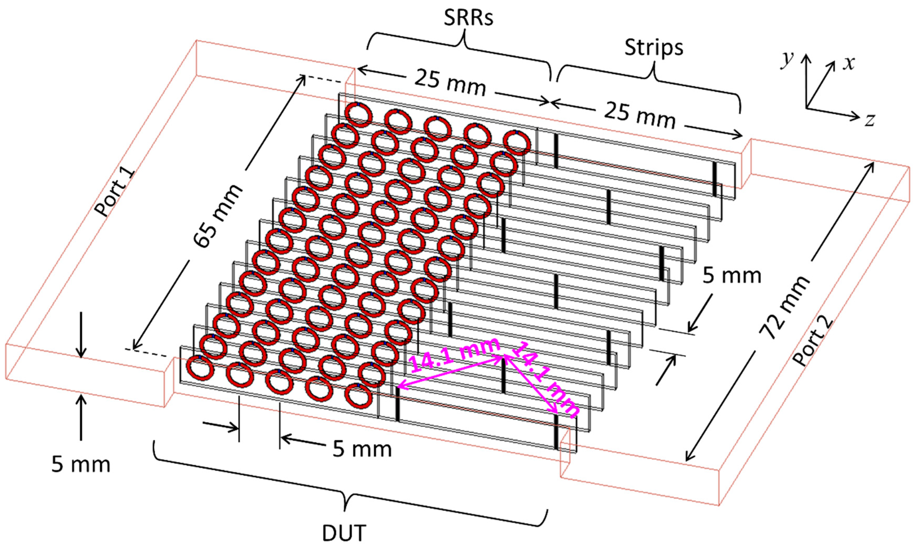
5. Description and Theoretical Analysis of Experimental Metamaterials

The purpose of this section is to show that tunneling is theoretically possible in accordance to the mechanism described in Section 2, for strip loaded and SRR loaded waveguides described in [24].

5.1. Description of Metamaterials

Figure 4 gives a rendering of the DUT (MNG and ENG loaded waveguide junction) of which one layer of thickness 5 mm (or one period of 5 mm in the y direction) is shown for clarity. To fill a WR284 waveguide used in the experiment, 7 layers (or 7 periods in the y direction) are required. Also shown are 72 mm wide waveguide feeds at either end which correspond to WR284 waveguide feeds used in the experiment. Both the SRR and strip loaded regions have a length of 25 mm and a width of 65 mm.
The MNG region comprises an array of SRRs aligned transverse to the waveguide to achieve negative permeability in the x-direction and will interact with the x component of magnetic field of the TE10 mode. The ENG region comprises y-directed strips to achieve negative permittivity in the y-direction thereby interacting with the TE10 mode electric field. This arrangement gives anisotropic permeability and permittivity [7,24] and field analysis given in Appendix C shows that tunneling described in Section 2 is indeed possible for such metamaterial junctions. The SRRs and strips are mounted on 13 printed circuit boards (PCBs) mounted parallel to the yz plane and are spaced 5 mm in the x direction to span a width of 65 mm. On the PCBs containing the SRRs, the SRRs have 5 mm periodicity in both directions and this means that within the SRR loaded waveguide, the SRRs have three-dimensional periodicity of 5 mm.
The design approach and the structural parameters of the SRRs and strips are described in detail elsewhere [24], but the key features are: (i) broadside-coupled SRRs were used as they are compact and minimize bianisotropy [29], (ii) the SRRs were designed to resonate around 3 GHz, (iii) uses a thinned array of strips to achieve suitable values of permittivity [24]. The strip locations have a two-dimensional periodicity of 14.1 mm in the xz plane, and their locations are coincident with the PCBs.

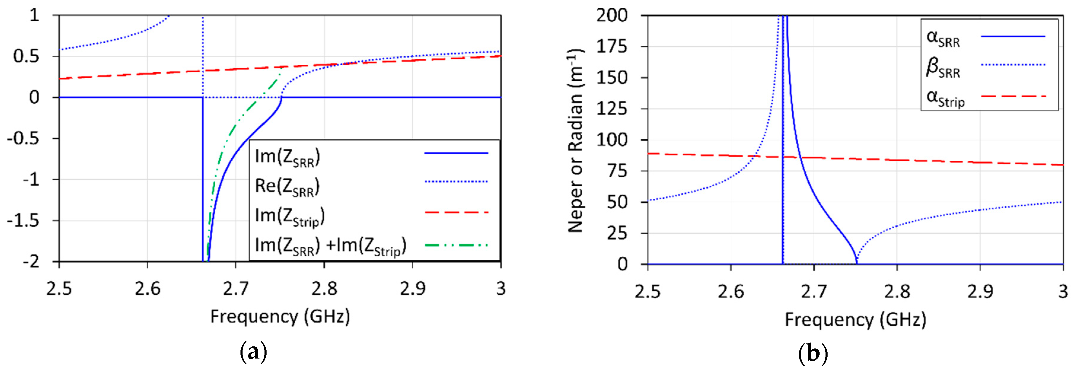
5.2. Theoretical Predictions

Theoretical models for the SRR and strip loaded waveguides are described in earlier work [24] and are used to predict the μXX and εYY of the SRR loaded waveguide, and εYY of the strip loaded waveguide. These models include electric polarization of the SRRs and dielectric loading due to the PCB substrates, and use the continuous medium approximation. The other tensor permeability and permittivity diagonal elements are equal to that of free-space, and the off-diagonal elements are zero. Figure 5 shows the frequency response of μXX and εYY of the SRR loaded waveguide, and εYY of the strip loaded waveguide over the frequency range 2.5 GHz to 3 GHz. It is apparent that SRR loading provides negative permeability over a narrow band (2.663 GHz to 2.752 GHz) and its value is strongly dependent on frequency. On the other hand, strip loading provides negative permittivity over a much wider frequency range and is a relatively weaker function of frequency.
Using the field analysis of Appendix C, the TE10 mode propagation constant and wave-impedance can be calculated from the anisotropic permittivity and permittivity (Figure 5), and are shown in Figure 6. The impedances are normalized to the TE10 mode wave-impedance of an empty 65 mm wide waveguide. As the strip loaded waveguide operates in its evanescent mode over the frequency range 2.5 GHz to 3 GHz, its real part of wave-impedance and phase constant are both zero over this range and are not shown. Importantly, the imaginary parts of wave-impedance are opposite signed over the frequency range 2.663 GHz to 2.752 GHz, and hence it is useful to show the sum Im ( Z S t r i p ) + Im ( Z S R R ) over the range 2.663 GHz to 2.752 GHz in Figure 6a.
The zero crossing of Im ( Z S t r i p ) + Im ( Z S R R ) in Figure 6a indicates that the impedance tunneling condition (2) is satisfied at 2.728 GHz. At this frequency, Figure 6b shows that the attenuation constants are 30.1 Np/m and 85.2 Np/m for the SRR and strip loaded waveguide respectively. If the length of the SRR loaded waveguide lMNG is 25 mm, then the strip loaded waveguide length lENG needs to be 8.9 mm to satisfy the attenuation tunneling condition (1). Figure 7 shows the calculated S-parameter frequency responses for the symmetrical structure of Figure 2 for the two cases (i) lMNG = 25 mm and lENG = 8.9 mm, and (ii) lMNG = 25 mm and lENG = 25 mm. It is apparent that for the former case, reflection-less transmission is obtained at 2.728 GHz. On the hand, the latter cases shows low coupling due to the non-satisfaction of the attenuation tunneling condition.
For the case of lENG equal to 8.9 mm, a very sharp peak in transmission is observed at 2.66 GHz. This frequency falls slightly outside the negative permeability band, and therefore, the SRR loaded waveguides behave as electrically long, high impedance transmission lines (see Figure 6). Due to the high electrical lengths in this vicinity, there will be a frequency (or multiple frequencies) where the length of the SRR loaded waveguides are integer multiples of a half guide-wavelength. In this situation, the SRR loaded waveguides behave as half-wave transformers effectively providing a direct coupling to the strip loaded waveguide to port 1 and 2. Due to the mismatch between the SRR loaded waveguide and empty waveguide wave-impedances, the resulting peak will be narrow. The total ENG length of Figure 2 is 17.8 mm (2lENG) and its attenuation is constant at 2.66 GHz is 86.3 Np/m. Hence, at 2.66 GHz its total attenuation will be 13 dB which is the level of transmission seen in Figure 7. The phenomenon is also denoted a Fabry-Perot resonance [7].

6. Experiment

6.1. Description of Metamaterials

The metamaterials described in Section 5.1 were fabricated using a multilayer PCB fabrication process on Rogers 4000 series substrates of which individual PCBs were mounted longitudinally in waveguide test fixtures. The PCB thickness was 0.5 mm. The PCBs were 25 mm × 36 mm and each type required to construct the MNG (SRR) and ENG (strip) regions is shown in Figure 8a. The rings of the SRRs use the middle metal layers but are visible through the translucent substrate, whilst the strips are placed on the top metal layer; the bottom metal layer is unutilized. The DUT is 50 mm long (lSRR = 25 mm and lStrip1 = 25 mm). The length of the strip loaded waveguide is 25 mm.

6.2. Waveguide PCB Mount

Figure 8b shows a photo of the waveguide PCB mount to hold the PCBs associated with the DUT. The one for the strip loaded waveguide is similar but shorter in length. When fully assembled, the waveguide mounts contain 13 longitudinal slots, with width equal to the PCB thickness (0.5 mm), and depth 1 mm, to hold the PCBs with 5 mm spacing across a width of 65 mm. The waveguide PCB mount mates with WR284 (72.14 mm × 34.04 mm) waveguide, and has transverse dimensions of 65 mm × 34 mm.
For manufacturability and to aid inserting PCBs, the waveguide mount is constructed from laminations. Transverse bolts along with the laminated nature of the test fixture, creates a vice to secure the PCBs in the slots. Due to manufacturing tolerances, it is impossible to machine laminations to exactly the same longitudinal length. To ensure continuity of waveguide longitudinal currents (in top and bottom walls) 0.5 mm deep recesses are milled at each end of the mount to create very low impedance RF chokes with the WR284 flanges.

6.3. Measurement Procedure

Measurements were performed over the band 2 GHz to 4 GHz using a Keysight N9918A RF vector network analyzer (Figure 8c) calibrated to SMA coaxial connector reference planes using the short-open-load-thru (SOLT) procedure. To eliminate effects coax-to-waveguide transitions, through-line (TL) deembedding [30] (which is related to TRL deembedding) was conducted offline to obtain the S-parameters for the various loaded waveguide PCB mounts. These measurements are available as Supplementary Materials. The reference planes were then extended by 0.5 mm to remove the effect of the RF chokes at the ends of the waveguide PCB mounts. The S-parameters were finally renormalized from the wave-impedance of an empty 72 mm wide (WR284) waveguide to that of an empty 65 mm wide (waveguide mount) waveguide. As the TE10 mode cut-off frequency of the 65 mm wide waveguide is 2.31 GHz, only measurements above this frequency are useful.

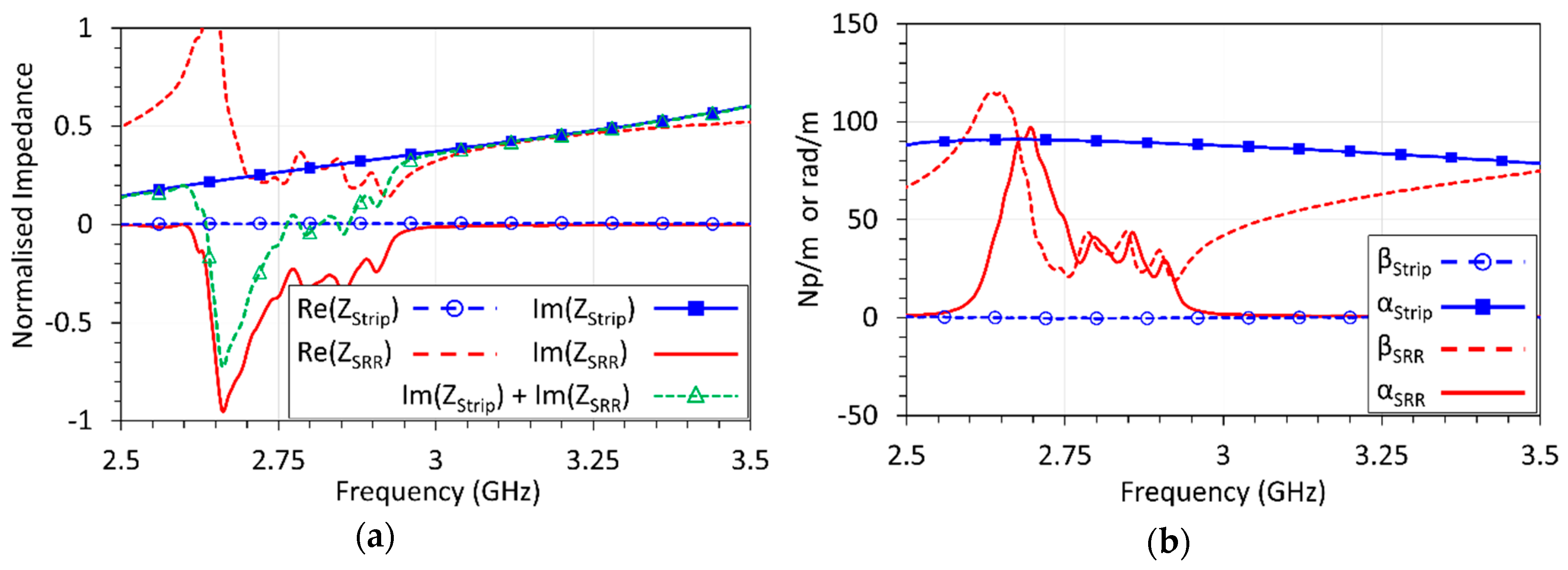
6.4. Strip and SRR Loaded Waveguide

Figure 9 shows the attenuation and phase constants, and wave-impedance extracted from the strip loaded waveguide measurements over the range 2.5 GHz to 3.5 GHz. The wave-impedance is normalized to the wave-impedance of an empty 65 mm waveguide. For completeness, the attenuation and phase constants, and wave-impedance for a SRR loaded waveguide is also shown for qualitative purposes. The challenges of retrieval ambiguities [31,32,33,34,35] is not evident for the strip loaded waveguide, whereas it could be a factor for the SRR loaded waveguide at the lower end of the MNG passband.
Figure 9 shows that the strip loaded waveguide behaves like an ideal evanescent-mode attenuator with an essentially zero phase constant (β) and pure imaginary characteristic impedance over the entire frequency range of interest. The SRR loaded waveguide has almost pure-real wave-impedance and near-zero attenuation constant (α), when operating below about 2.6 GHz and above about 2.95 GHz, and it therefore operates in a propagating mode in these frequency bands. On the other hand, between about 2.65 GHz and 2.95 GHz, it behaves as a lossy evanescent-mode attenuator with complex valued propagation constant and wave-impedance. This lossy behavior is attributed to losses in the SRRs which are operating near resonance [24].
Although it is difficult to make use of the SRR loaded waveguide data directly, it never-the-less can be qualitatively interpreted as evidence of MNG behavior over the range 2.65 GHz to 2.95 GHz. For instance, αSRR and imaginary part of ZSRR are both non-zero, over this range. Figure 9a also shows that the sum of Im(ZStrip) and Im(ZSRR), crosses zero at several frequencies over the range 2.76 GHz to 2.86 GHz; meaning that the impedance tunneling condition (4) will be satisfied in the imaginary part within this range. In an ideal situation, the impedance matching condition (4) is satisfied at one frequency only, so the multiple zeros of Im ( Z S t r i p ) + Im ( Z S R R ) in Figure 9a is due to SRR resonant frequency variation across the PCB panels [36].

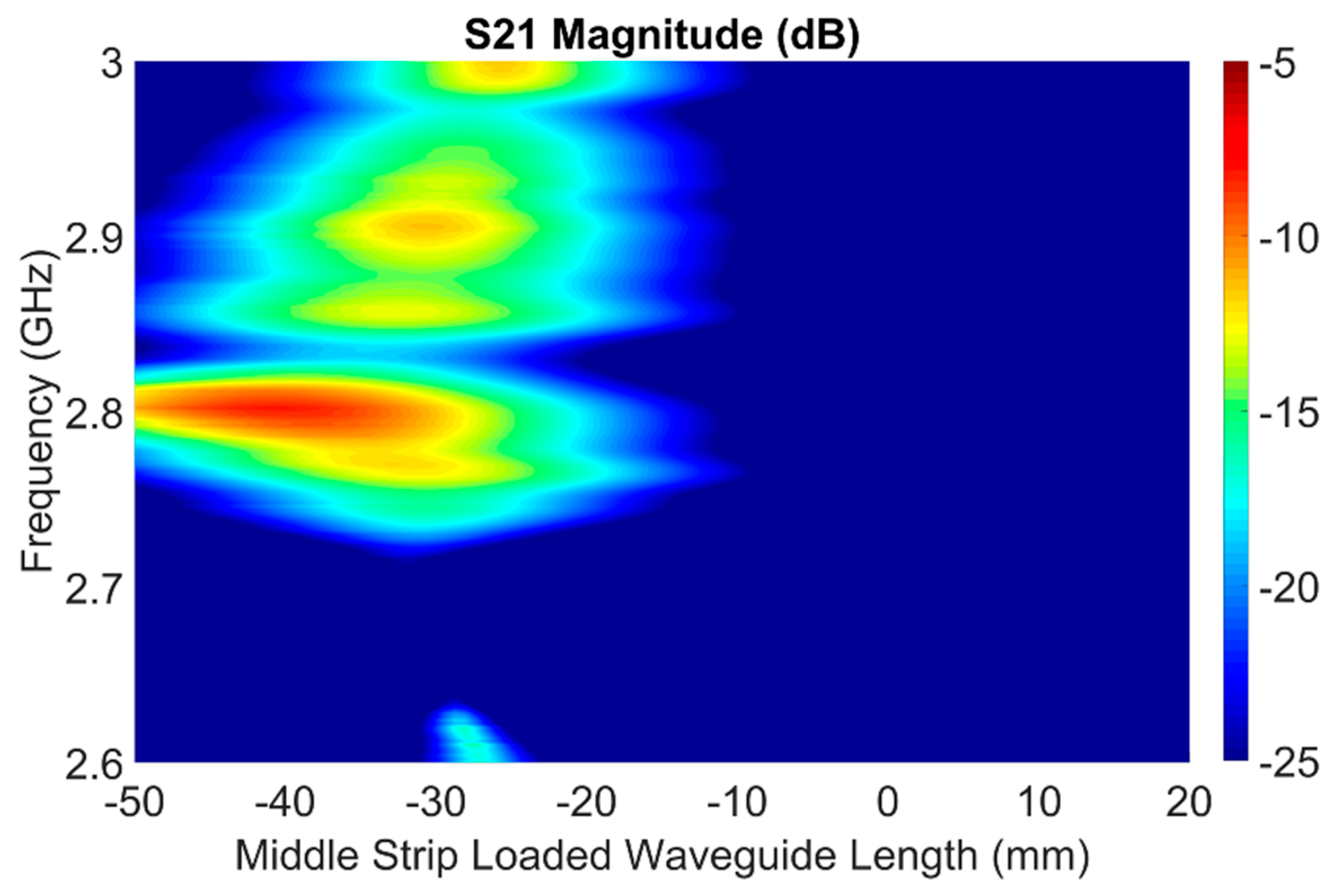
6.5. Tunnel Identification

The tunnel identification method described in Section 4 was applied to the DUT measurements. Figure 10 shows the transmission (S21) as a function of frequency (f) and middle strip loaded waveguide section length (lStrip2). Transmission is maximum at 2.8 GHz, and peaks when lStrip2 is −40.8 mm. The lStrip2 value of −40.8 mm means that the total length of the equivalent strip loaded section of Figure 3b, ( 2 l S t r i p 1 + l S t r i p 2 ) , is 9.2 mm. This value is comparable to the theoretical prediction of 17.8 mm given in Section 5.
Figure 11 shows the S-parameters of the cascaded structure of Figure 3a when lStrip2 is equal to −40.8 mm. For reference, the S-parameters of the DUT are shown. At 2.8 GHz, the tunneling effect is clearly revealed with an 8.6 dB boost in transmission (S21) compared to the DUT on its own, as well as in improvement of input and output match. Importantly, the resulting S-parameters are symmetric (S11 = S22).
For a symmetrical reciprocal two-port, the power loss proportion, L, can be calculated by power conservation:
L = 1 | S 11 | 2 | S 21 | 2 = 1 | S 22 | 2 | S 12 | 2
where S11, S22, S12 and S21 are the S-parameters of the two-port. Figure 12 shows the power loss of the DUT after tunnel identification. Significant loss occurs within the MNG band and this explains the insertion loss of 8.1 dB at 2.8 GHz after the tunnel identification process of Section 3. The effects of losses can be removed from the symmetric two-port by scaling the S-parameters by 1 / 1 L . With the effects of losses are removed (pink dashed trace in Figure 11), the resulting tunnel residual insertion loss, due to mismatch, is 2.2 dB.

7. Other Observations

After the tunnel identification method has been applied, a significant transmission boost occurs at 2.45 GHz and 3.3 GHz (blue trace in Figure 11). Both these frequencies fall well outside the MNG regime of the SRR loaded waveguide and therefore cannot be attributed to tunneling. At these frequencies, the SRR loaded waveguide behaves as a transmission line that transform the empty waveguide characteristic impedance to a complex value, and at the same time, the strip loaded waveguide essentially behaves as a lossless evanescent mode attenuator. The strip-loaded waveguide can be treated as a two-port element terminated by complex valued impedances. From microwave amplifier design principles [37], this situation may result in a boost in transmission because of the non-trivial dependence on terminating impedance.
When loss is removed, a sharp peak is also revealed at 2.636 GHz (pink trace in Figure 11a). Figure 9 indicates that this frequency is slightly outside the MNG band of frequencies and therefore, this peak is attributed to Fabry-Perot resonances [7] as discussed in the theoretical investigation in Section 5. This resonance is obscured after tunnel identification (blue trace in Figure 11) as the loss at this frequency (Figure 12), is nearly 100%.

8. Conclusions

Due to the finite size of constituent elements and losses, the ability to experimentally demonstrate tunneling across a cascade of mu-negative and epsilon-negative loaded waveguides may be hindered. A tunnel identification method has been developed and demonstrated to reveal the tunneling behavior that is otherwise obscured. The S-parameters of a mu-negative/epsilon-negative loaded waveguide junction are combined with the S-parameters of an epsilon-negative loaded waveguide. The method yields symmetric S-matrices, which the effect of losses to be removed to provide a yet clearer demonstration of tunneling.

Supplementary Materials

The measured S-parameters, after applying TL deembeding to WR284 waveguide flange reference planes, are available online at https://www.mdpi.com/2079-9292/8/1/84/s1 as .s2p files. In the case of the SRR and Strip loaded waveguide, symmetry is enforced in the deembedding process. In all cases, the reference impedance is the TE10 mode wave-impedance of a 72 mm wide waveguide. Therefore, prior to further processing, it is necessary to shift the reference planes 0.5 mm and renormalize the reference impedance of that of a 65 mm waveguide.

Author Contributions

Conceptualization, K.W.E. and I.G.P. Methodology, K.W.E.; Software, K.W.E.; Investigation, K.W.E.; Resources, I.G.P.; Data curation, K.W.E.; Writing—original draft preparation, K.W.E.; Writing—review and editing, K.W.E. and I.G.P.; Project administration, I.G.P.; Funding acquisition, I.G.P.

Funding

This work was funded by the New Zealand Ministry of Business, Innovation and Employment (Research contract no. LVLX1505).

Acknowledgments

The authors would like to thank student intern F. Flamein, of Graduate School of Chemistry, Biology and Physics (ENSCBP): Bordeaux Institute of Technology (Bordeaux INP), for assistance in the conduct of experiments, R Cook of Lincoln Agritech Ltd. for fabricating the waveguide test fixtures, and their colleagues A. Tan and I. M. Woodhead for useful discussions.

Conflicts of Interest

The authors declare no conflict of interest. The funders had no role in the design of the study; in the collection, analyses, or interpretation of data; in the writing of the manuscript, or in the decision to publish the results.

Appendix A

In this appendix, the dispersion relations for a lossless isotropic ENG or MNG loaded waveguide are obtained. The field analysis of an air-filled waveguide can be extended to a dielectric filled waveguide [23], with permeability μ and permittivity ε, and the resulting propagation constant (γ) and wave-impedance (Z) are:
γ 2 = k x 2 ω 2 μ ε
and
Z = j ω μ γ
where kx is the mode cut-off wavenumber, which for TEm0 modes in a waveguide of width a are:
k x = m π a
where m is a non-zero integer.
For a given mode, a transmission line analogy can be used to represent a section of waveguide [23]. For the case of a uniform cross-section, the propagation constant and characteristic impedance of the transmission line use γ and wave-impedance Z respectively.
For a lossless MNG or ENG, either μ or ε will be negative valued and the other positive, and (A1) shows that γ only takes pure real values and means that only evanescent modes are possible. Equation (A2) indicates that Z will be pure imaginary and capacitive for MNG, and inductive for ENG.

Appendix B

In this appendix, the tunneling conditions derivation are derived. This derivation is based upon voltage-current chain or ABCD parameters [23] noting this problem can that alternatively formulated using wave-transmission parameters [7].
We consider the cascade of a pair of waveguide sections with identical transverse cross sections and therefore the only discontinuity is due to the different materials that fill each of these sections. These two sections could correspond to Section 2 and Section 3 of Figure 1 which contain MNG and ENG fills respectively. As both sections are operating in their evanescent modes, they can be described by a pure real propagation constant (being the attenuation constant) and a pure imaginary wave-impedance α1 and jX1 respectively for Section 1, α2 and jX2 respectively for Section 2. The values of α1 and α2 are assumed to take positive values for passive media, whereas the X1 and X2 can take positive and negative values. For a given mode, a section of waveguide can be modelled as a transmission line described by its propagation constant and characteristic impedance. Using an ABCD parameter formulation [23], the ABCD matrix of the cascade of the two waveguide sections of lengths l1 and l2 is:
A B C D c a s c a d e = [ cosh ( α 1 l 1 ) j X 1 sinh ( α 1 l 1 ) 1 j X 1 sinh ( α 1 l 1 ) cosh ( α 1 l 1 ) ] [ cosh ( α 2 l 2 ) j X 2 sinh ( α 2 l 2 ) 1 j X 2 sinh ( α 2 l 2 ) cosh ( α 2 l 2 ) ]
Expanding:
A B C D c a s c a d e = [ cosh ( α 1 l 1 ) cosh ( α 2 l 2 ) + X 1 X 2 sinh ( α 1 l 1 ) sinh ( α 2 l 2 ) 1 j X 2 sinh ( α 2 l 2 ) cosh ( α 1 l 1 ) + 1 j X 1 sinh ( α 1 l 1 ) cosh ( α 2 l 2 )        j X 2 sinh ( α 2 l 2 ) cosh ( α 1 l 1 ) + j X 1 sinh ( α 1 l 1 ) cosh ( α 2 l 2 ) cosh ( α 1 l 1 ) cosh ( α 2 l 2 ) + X 2 X 1 sinh ( α 1 l 1 ) sinh ( α 2 l 2 ) ]
An identity ABCD corresponds to perfect transmission with zero reflection. Equation (A5) is equal to the identity matrix when α 1 l 1 = α 2 l 2 and X 1 = X 2 which are denoted the attenuation and impedance tunneling conditions respectively. The latter condition requires X1 and X2 to be opposite signed and represents resonance across the boundary between Section 1 and Section 2 [6,8].

Appendix C

In this appendix, the fields are formulated for TEm0 modes in a rectangular waveguide filled with anisotropic dielectrics. The outcome of this analysis is the attenuation constant and wave-impedance for the special case of anisotropic ENG and MNG dielectric fill.
Consider an anisotropic dielectric material whose permeability and permittivity tensors in rectangular coordinates are respectively:
μ = [ μ x x 0 0 0 μ y y 0 0 0 μ z z ]
ε = [ ε x x 0 0 0 ε y y 0 0 0 ε z z ]
where μxx, μyy and μzz are the x, y and z directed permeability respectively, and εxx, εyy and εzz are the x, y and z directed permittivity respectively. It is therefore assumed that the material is non-bianisotropic, non-gyrotropic and non-chiral which give zero off-diagonal elements. This assumption is reasonable for the types of metamaterials considered in this work comprising either broad-side-coupled SRRs, or thin strips.
Consider a rectangular waveguide directed in the z direction and whose perfect-electric-conducting walls are located at x = 0, x = a, y = 0 and y = b. All field component phasors of a wave propagating in the z direction will contain the common factor exp(-γz) where γ is the complex valued propagation constant. If we restrict the waves to be TE (transverse electric) waves, and further restrict the wave to containing no y dependence (i.e., TEm0 modes), substitution of (A6) and (A7) into Maxwell’s curl equations in phasor form, yields:
γ E y = j ω μ x x H x
E y x = j ω μ z z H z
γ H x H z x = j ω ε y y E y
Equations (A8a)–(A8c) shows that only the tensor components μxx, εyy and μzz play a role in TEm0 mode behavior. Based upon the waveguide boundary conditions, the solution of the non-zero field phasors, that also satisfy (A8a) and (A8b) must take the form:
H x = γ A j ω μ x x sin k x x
E y = A sin k x x
H z = k x A j ω μ z z cos k x x
where the cut-off wavenumber kx is given by (A3), A is an amplitude (which could be complex valued), and m is a non-zero integer. Substituting (A9) into (A8c) yields the dispersion relation:
γ 2 = μ x x μ z z k x 2 ω 2 μ x x ε y y
For an evanescent mode, γ will be pure real and equal to the attenuation constant α which is positive valued. For a TE wave travelling (or decaying) in the z direction, the wave-impedance is E y / H x . Hence from (A9a) and (A9b):
Z T E = j ω μ x x α
Thus from (A11), ZTE will be pure imaginary whose is sign is that of μxx.
There are two types of anisotropic dielectric that are of interest here. They are MNG with negative permeability confined to the x direction, and ENG with negative permittivity confined to the y direction.

C.1. Anisotropic MNG

For the first case, μxx is negative valued, μzz equals μ0 the permeability of a vacuum, and εyy is positive valued. The permittivity εyy is greater than the permittivity of a free-space (ε0) due to the inherent electric polarizability of the constituent elements comprising the metamaterial, and the presence of insulating substrates to support such elements. Hence, from (A10):
α = μ x x μ 0 ( ω 2 μ 0 ε y y k x 2 )
and is real (i.e., evanescent mode) only if ω 2 μ 0 ε y y > k x 2 which is denoted the “anti-cut-off” property [7]. Clearly from (A11), ZTE will be a capacitive reactance.

C.2. Anisotropic ENG

For the second case, μxx = μzz = μ0, and εyy is negative valued. Hence, from (A10):
α = k x 2 ω 2 μ 0 ε y y
and is real for all frequencies provided εyy is negative valued. Clearly from (A11), ZTE will be an inductive reactance.
The foregoing indicates that pairing of the above anisotropic ENG and MNG filled waveguides can yield the required impedance tunneling condition. Namely, apart from the anti-cut-off property, the conclusions are similar to the isotropic ENG and MNG cases.
In practice, for SRR realizations of anisotropic MNG, and strip realization of ENG, μxx and εyy are frequency dependent and are only negative over a restricted frequency range; particularly for the SRR loaded waveguide. Therefore, the above theoretical analysis needs to be interpreted in that context.

References

  1. Silveirinha, M.; Engheta, N. Tunneling of electromagnetic energy through subwavelength channels and bends using ε-near-zero materials. Phys. Rev. Lett. 2006, 97, 157403. [Google Scholar] [CrossRef] [PubMed]
  2. Liu, R.; Cheng, Q.; Hand, T.; Mock, J.J.; Cui, T.J.; Cummer, S.A.; Smith, D.R. Experimental demonstration of electromagnetic tunneling through an epsilon-near-zero metamaterial at microwave frequencies. Phys. Rev. Lett. 2008, 100, 023903. [Google Scholar] [CrossRef] [PubMed]
  3. Edwards, B.; Alù, A.; Young, M.E.; Silveirinha, M.; Engheta, N. Experimental verification of epsilon-near-zero metamaterial coupling and energy squeezing using a microwave waveguide. Phys. Rev. Lett. 2008, 100, 033903. [Google Scholar] [CrossRef] [PubMed]
  4. Mitrovic, M.; Jokanovic, B.; Vojnovic, N. Wideband tuning of the tunneling frequency in a narrowed epsilon-near-zero channel. IEEE Antennas Wirel. Propag. Lett. 2013, 12, 631–634. [Google Scholar] [CrossRef]
  5. Soric, J.C.; Alù, A. Longitudinally independent matching and arbitrary wave patterning using ε-near-zero channels. IEEE Trans. Microw. Theory Tech. 2015, 63, 3558–3567. [Google Scholar] [CrossRef]
  6. Alù, A.; Engheta, N. Pairing an epsilon-negative slab with a mu-negative slab: Resonance, tunneling and transparency. IEEE Trans. Antennas Propag. 2003, 51, 2558–2571. [Google Scholar] [CrossRef] [Green Version]
  7. Baena, J.D.; Jelinek, L.; Marqués, R.; Medina, F. Near-perfect tunneling and amplification of evanescent electromagnetic waves in a waveguide filled by a metamaterial: Theory and experiments. Phys. Rev. B 2005, 72, 075116. [Google Scholar] [CrossRef]
  8. Liu, R.; Zhao, B.; Lin, X.Q.; Cheng, Q.; Cui, T.J. Evanescent-wave amplification studied using a bilayer periodic circuit structure and its effective medium model. Phys. Rev. B 2007, 75, 125118. [Google Scholar] [CrossRef]
  9. Feng, Y.; Teng, X.; Wang, Z.; Zhao, J.; Jiang, T. Extraordinary transmission with evanescent wave enhancement in planar waveguide loaded with anisotropic metamaterials. In Proceedings of the 2008 Asia–Pacific Microwave Conference, Hong Kong/Macao, China, 16–20 December 2008; IEEE: New York, NY, USA, 2008. [Google Scholar] [CrossRef]
  10. Feng, T.; Li, Y.; Jiang, H.; Sun, Y.; He, L.; Li, H.; Zhang, Y.; Shi, Y.; Chen, H. Electromagnetic tunneling in a sandwich structure containing single negative media. Phys. Rev. E 2009, 79, 026601. [Google Scholar] [CrossRef]
  11. Liu, C.H.; Behdad, N. Analysis of electromagnetic wave tunneling through stacked single-negative metamaterial slabs: A microwave filter theory approach. In Proceedings of the 2012 IEEE International Symposium on Antennas and Propagation, Chicago, IL, USA, 8–14 July 2012; IEEE: New York, NY, USA, 2012. [Google Scholar] [CrossRef]
  12. Zhang, L.; Wang, J.; He, L.; Qiao, W.; Chen, L.; Wang, Q.; Zhao, Y. Tunneling time in a conjugate matched pair consisting of ε-negative and μ-negative materials. Physica B 2013, 431, 127–131. [Google Scholar] [CrossRef]
  13. Zhang, L.; Zhang, Y.; Chen, X.; Liu, X.; Zhang, L.; Chen, H. Study on the tunneling mode in a sub-wavelength open-cavity resonator consisting of single negative materials. IEEE Trans. Antennas Propag. 2014, 62, 504–508. [Google Scholar] [CrossRef]
  14. Zhao, J.; Zhang, Y.; Yu, X.; Li, Y.; He, L.; Fang, K. Electromagnetic tunneling through epsilon-negative waveguide paired with mu-negative waveguide. In Proceedings of the 2014 Asia-Pacific Conference on Antennas and Propagation, Harbin, China, 26–29 July 2014; IEEE: New York, NY, USA, 2014. [Google Scholar] [CrossRef]
  15. Chen, Y.; Huang, S.; Yan, X.; Shi, J. Electromagnetic tunneling through conjugated single-negative metamaterial pairs and double-positive layer with high-magnetic fields. Chin. Opt. Lett. 2014, 12, 101601. [Google Scholar] [CrossRef]
  16. Marques, R.; Martel, J.; Mesa, F.; Medina, F. Left-handed-media simulation and transmission of EM waves in subwavelength split-ring-resonator-loaded metallic waveguides. Phys. Rev. Lett. 2002, 89, 183901. [Google Scholar] [CrossRef]
  17. Hrabar, S.; Bartolic, J.; Sipus, Z. Waveguide miniaturization using uniaxial negative permeability metamaterial. IEEE Trans. Antennas Propag. 2005, 53, 110–119. [Google Scholar] [CrossRef]
  18. Odabasi, H.; Teixeira, F.L. Electric-field-coupled resonators as metamaterial loadings for waveguide miniaturization. J. Appl. Phys. 2013, 114, 214901. [Google Scholar] [CrossRef] [Green Version]
  19. Pollock, J.G.; Iyer, A.K. Below-cutoff propagation in metamaterial-lined circular waveguides. IEEE Trans. Microw. Theory Tech. 2013, 61, 3169–3178. [Google Scholar] [CrossRef]
  20. Esteban, J.; Camacho-Peñalosa, C.; Page, J.E.; Martín-Guerrero, T.M.; Márquez-Segura, E. Simulation of negative permittivity and negative permeability by means of evanescent waveguide modes—Theory and experiment. IEEE Trans. Microw. Theory Tech. 2005, 53, 1506–1514. [Google Scholar] [CrossRef]
  21. Pendry, J.B.; Holden, A.J.; Robbins, D.J.; Stewart, W.J. Low frequency plasmons in thin-wire structures. J. Phys. Condens. Matter 1998, 10, 4785–4809. [Google Scholar] [CrossRef] [Green Version]
  22. Pendry, J.B.; Holden, A.J.; Robbins, D.J.; Stewart, W.J. Magnetism from conductors and enhanced nonlinear phenomena. IEEE Trans. Microw. Theory Tech. 1999, 47, 2075–2084. [Google Scholar] [CrossRef] [Green Version]
  23. Ramo, S.; Whinnery, J.R.; van Duzer, T. Fields and Waves in Communication Electronics; John Wiley & Sons, Inc.: New York, NY, USA, 1994; ISBN 0-471-58551-34. [Google Scholar]
  24. Eccleston, K.W.; Platt, I.G. Printed NRI metamaterial based on broad-side-coupled SRRs and a thinned array of strips. In Proceedings of the 2016 Asia-Pacific Microwave Conference, New Delhi, India, 5–9 December 2016; IEEE: New York, NY, USA, 2017. [Google Scholar] [CrossRef]
  25. Smith, D.R.; Padilla, W.J.; Vier, D.C.; Nemat-Nasser, S.C.; Schultz, S. Composite medium with simultaneously negative permeability and permittivity. Phys. Rev. Lett. 2000, 84, 4184–4187. [Google Scholar] [CrossRef]
  26. Pozar, D.M. Microwave Engineering, 3rd ed.; John Wiley & Sons Inc.: Hoboken, NJ, USA, 2005; ISBN 978-0-470-63155-3. [Google Scholar]
  27. Eberspächer, M.A.; Eibert, T.F. Extraction of embedded dispersion characteristics. In Proceedings of the 2011 Asia-Pacific Microwave Conferenc, Melbourne, Australia, 5–8 December 2011; IEEE: New York, NY, USA, 2011; pp. 801–804. [Google Scholar]
  28. Williams, D.F.; Jargon, J.; Arz, U.; Hale, P. Rectangular-waveguide impedance. In Proceedings of the 85th ARFTG Conference, Phoenix, AZ, USA, 22 May 2015; IEEE: New York, NY, USA, 2015. [Google Scholar] [CrossRef]
  29. Marqués, R.; Mesa, F.; Martel, J.; Medina, F. Comparative analysis of edge-and broadside-coupled split ring resonators for metamaterial design-theory and experiments. IEEE Trans. Antennas Propag. 2003, 51, 2572–2581. [Google Scholar] [CrossRef]
  30. Eccleston, K.W. A new interpretation of through-line deembedding. IEEE Trans. Microw. Theory Tech. 2016, 64, 3887–3893. [Google Scholar] [CrossRef]
  31. Baskey, H.B.; Akhtar, M.J. An improved measurement technique for retrieval of effective constitutive properties of thin dielectric/magnetic and metamaterial samples. In Proceedings of the 83rd ARFTG Microwave Measurement Conference, Tampa, FL, USA, 6 June 2014; IEEE: New York, NY, USA, 2014. [Google Scholar] [CrossRef]
  32. Hrabar, S.; Benic, L.; Bartolic, J. Simple experimental determination of complex permittivity or complex permeability of SNG metamaterials. In Proceedings of the 36th European Microwave Conference, Manchester, UK, 10–15 September 2006; IEEE: New York, NY, USA, 2006; pp. 1395–1398. [Google Scholar] [CrossRef]
  33. Chen, H.; Zhang, J.; Bai, Y.; Luo, Y.; Ran, L.; Jiang, Q.; Kong, J.A. Experimental retrieval of the effective parameters of metamaterials based on a waveguide method. Opt. Express 2006, 14, 12944–12949. [Google Scholar] [CrossRef] [PubMed]
  34. Kim, S.; Kuester, E.F.; Holloway, C.L.; Scher, A.D.; Baker-Jarvis, J. Boundary effects on the determination of metamaterial parameters from normal incidence reflection and transmission measurements. IEEE Trans. Antennas Propag. 2011, 59, 2226–2240. [Google Scholar] [CrossRef]
  35. Arslanagić, S.; Hansen, T.V.; Mortensen, N.A.; Gregersen, A.H.; Sigmund, O.; Ziolkowski, R.W.; Breinbjerg, O. A review of the scattering-parameter extraction method with clarification of ambiguity issues in relation to metamaterial homogenization. IEEE Antennas Propag. Mag. 2013, 55, 91–106. [Google Scholar] [CrossRef]
  36. Machac, J.; Jelinek, L. Metamaterial made of BC-SRRs with randomly dispersed resonance frequencies. In Proceedings of the 2015 IEEE MTT-S International Microwave Symposium, Phoenix, AZ, USA, 17–22 May 2015; IEEE: New York, NY, USA, 2015. [Google Scholar] [CrossRef]
  37. Gonzalez, G. Microwave Transistor Amplifiers—Analysis and Design, 2nd ed.; Prentice-Hall: Upper Saddle River, NJ, USA, 1997; ISBN 0-13-254335-4. [Google Scholar]
Figure 1. Schematic of a cascade of MNG and ENG metamaterial filled waveguide where tunneling (transmission from port 1 to port 2 or vice versa) is possible under certain conditions. (In color.).
Electronics 08 00084 g001
Figure 2. Schematic of a cascade of MNG, ENG and MNG metamaterial filled waveguide where tunneling (transmission from port 1 to port 2 or vice versa) is possible under certain conditions. (In color.).
Electronics 08 00084 g002
Figure 3. Block diagram of the tunneling identification method: (a) constituent elements, and (b) equivalent structure.
Electronics 08 00084 g003
Figure 4. Rendering of one layer of the DUT containing the SRR array (MNG)/strip array (ENG) interface. (In color.).
Electronics 08 00084 g004
Figure 5. Theoretical predictions of anisotropic permittivity and permeability for the SRR and strip loaded waveguides of the type considered in this work. (In color.).
Electronics 08 00084 g005
Figure 6. Theoretically calculated TE10 mode (a) normalized wave-impedance, (b) attenuation and phase constants for strip and SRR loaded waveguide. (In color.).
Electronics 08 00084 g006
Figure 7. Theoretically predicted TE10 mode S-parameters for the structure of Figure 2 using anisotropic permittivity and permeability values of Figure 5 for the two cases of lENG when lMNG is 25 mm. (In color.).
Electronics 08 00084 g007
Figure 8. Photo of: (a) each PCB type used in the experiment, (b) the waveguide PCB mount, and (c) measurement equipment shown measuring the through configuration for TL deembedding. (In color.).
Electronics 08 00084 g008
Figure 9. Extracted TE10 mode (a) normalized wave-impedance, (b) attenuation and phase constants for strip and SRR loaded waveguide. (In color.).
Electronics 08 00084 g009
Figure 10. Transmission (S21) magnitude versus frequency and length of the middle strip loaded waveguide (lStrip2). Peak transmission occurs at 2.8 GHz when the length of the middle strip loaded waveguide (lStrip2) is −40.8 mm. (In color.).
Electronics 08 00084 g010
Figure 11. S-parameter magnitude frequency responses after tunnel identification and after loss is removed: (a) S21, and (b) S11 (and S22). The DUT response is included for comparison. (In color.).
Electronics 08 00084 g011
Figure 12. Power loss frequency response for the deembedded DUT.
Electronics 08 00084 g012

