The Relevance of Point Defects in Studying Silica-Based Materials from Bulk to Nanosystems
by
 , , and
Antonino Alessi
1,* ,
,
Jochen Kuhnhenn
1,
Gianpiero Buscarino
2,
Diego Di Francesca
3 and
Simonpietro Agnello
2 1
Fraunhofer Institute for Technological Trend Analysis INT, Business Unit Nuclear Effects in Electronics and Optics, Appelsgarten 2, 53879 Euskirchen, Germany
2
Università degli Studi di Palermo, Dipartimento di Fisica e Chimica-Emilio Segrè, Via Archirafi 36, 90123 Palermo, Italy
3
European Organization for Nuclear Research (CERN), CH-1211 Geneva 23, Switzerland
*
Author to whom correspondence should be addressed.
Electronics 2019, 8(12), 1378; https://doi.org/10.3390/electronics8121378
Submission received: 9 October 2019
/
Revised: 15 November 2019
/
Accepted: 18 November 2019
/
Published: 20 November 2019
(This article belongs to the Section Microelectronics)
Abstract
:The macroscopic properties of silica can be modified by the presence of local microscopic modifications at the scale of the basic molecular units (point defects). Such defects can be generated during the production of glass, devices, or by the environments where the latter have to operate, impacting on the devices’ performance. For these reasons, the identification of defects, their generation processes, and the knowledge of their electrical and optical features are relevant for microelectronics and optoelectronics. The aim of this manuscript is to report some examples of how defects can be generated, how they can impact device performance, and how a defect species or a physical phenomenon that is a disadvantage in some fields can be used as an advantage in others.
1. Introduction
Silica (amorphous SiO2) is a widely employed material in microelectronics and optoelectronics. It is present in MOS (metal–oxide–semiconductor) and SOI (silicon-on-insulator) technologies [1,2,3,4,5], see Figure 1a,b for their basic representations; it is the basic material of optical fibers [5,6,7,8,9,10] (Figure 1c illustrates a basic representation of an optical fiber) and of several bulk systems as lenses and mirrors [6,11,12]. Furthermore, nanocomposite materials containing silica have been proposed for different applications [13,14,15,16]; Figure 1d illustrates a scheme of pure silica non-porous nanoparticles and its features. The extensive use of silica is related to its availability and its dielectric and optical properties such as the large optical band gap. In a large number of investigations, it was reported that point defects can modify the silica properties or can affect the performance of a specific device. To better understand the nature of these defects in an amorphous material such as silica, it is important to remember that (i) a basic unit of silica has a tetrahedron with an Si atom in the center and an O atom in each of the four corners (see Figure 2a), and (ii) that such a unit is comparable to that present in the crystalline α-quartz form, being the amorphous status related to the distribution of inter-tetrahedral parameters such as the Si–O–Si angle [6], as highlighted by the blue arc in Figure 2a. With this in mind, a point defect can be considered as a deviation from the basic unit structure. In other words, any broken bond, missing or substitutional atom, as well as interstitial molecular or atomic species, are defects [6]. Furthermore, in many cases, strained bonds can be considered defects, too. A relevant variation of the Si–O bond length is itself a deviation from the basic unit. Obviously, it is important to define how large this variation should be to be considered a deviation in a material that presents a certain distribution of this parameter, although small in comparison to the distribution of the Si–O–Si angle [6]. However, since such strained bonds are considered precursors of other defects having a large impact in electronics and optics, they deserve to be considered as defects [9,17,18,19,20,21,22,23,24]. To understand how the point defects are important in the above cited application fields, we should remember that (i) they can be neutral, positively, or negatively charged, (ii) they can be paramagnetic or diamagnetic, and that (iii) in general, they are optically active. Indeed, their corresponding electronic states have energy levels within the band gap. As a consequence of this, they introduce absorption and emission transitions with energy lower than the band gap. Figure 2b illustrates a couple of energy levels of a point defect, from which absorption and emission activities originate.
In the field of study of the radiation response of optical fibers, such effects are at the origin of the RIA (radiation-induced attenuation) and the RIE (radiation-induced emission) [7,9]. In addition to these effects, we should also remember that as a consequence of the Kramers–Kronig relations [25], any kind of point defect induces changes in the refractive index, even simply through its absorption. Such variations, albeit small, can be sufficient to affect the optical fiber operation. However, refractive index variations are not necessarily a disadvantage when kept under control [6,25,26]. While the study of the radiation response of a device containing silica is strictly related to the defects, these defects can be relevant also when irradiation is not present. A clear example of this is constituted by the Si–OH defects for telecommunication fibers [27] and nanoparticles [13,28,29].
The aim of the present manuscript is to present some examples of the impact of point defects in different applications including, but not limited to, optoelectronic devices such as fibers. The paper also aims to put in evidence that it is possible to consider the defects and their effects on silica as an advantage or a disadvantage depending on the application. Looking at this double nature of the defects, it is possible to transform a problem for an application in a solution for another. Finally, we will also report some examples regarding how the defects were used for the improvement of basic research topics. Such deep understanding is useful for an approach that wants to transform a problem into a solution.
2. Non-Porous Silica Nanoparticles
In Figure 1d, we listed the different properties of the silica nanoparticles. This paragraph briefly summaries how they were obtained. From this short summary, the readers can note how the large use of the study of defects can help to infer the features of the investigated system. The model of a surface and core shells with different structures in terms of density and ring statistics was proposed by simulation in [30]. Subsequently, [31,32] have supported the differences between these two parts of the nanoparticles by employing structural investigation techniques such as Raman scattering [31], but also studying the properties of point defects performing electron paramagnetic resonance (EPR) experiments [32]. Then, to support the independence from the nanoparticle sizes, systematic studies were performed on particles going from average diameters of 7 to 40 nm [33,34,35,36,37,38,39]. The emission and the Raman signal of interstitial oxygen molecules [33,34] were studied showing that these molecules are present in the core, whereas the surface (rich of OH groups [33]) is unable to retain these small molecules. The density of the core was proved to be slightly higher (~4%) [35] than that of bulk silica, using the relation between density and some EPR spectral features of the E’Si [6] (see paragraph 4). Such a result, in agreement with the simulation [30], was supported by the Raman data [36]. Furthermore, the concentrations of defects such as E´Si, NBOHC (non-bridging oxygen hole centers) [6], and others were used to investigate other properties of the nanoparticles [33,34,35,36,37,38,39,40,41]. From the data reported in [33,34,35,36,37,38], the surface shell thickness was estimated to be ~1 nm, and it was also characterized by studying the visible emission related to surface point defects [38,39,40,41].
3. Generation of Defects
There are several processes that lead to the formation of point defects, or in which the generation of defects is involved [6,7,9,12]. Any of these processes imply complex and basic considerations of the solid-state physics and of the radiation matter interaction [6,12]. In this section, we will discuss some general aspects.
For the manufacturing of any material, including silica, the purity of the raw materials and their contamination during growth are key factors [6]. For both of these, the result is the introduction of point defects. Such defects are called extrinsic, since they are related to chemical species different from Si and O in the case of silica [6]. For the aim of the present paper, it is worth noting the SiOH groups and the Cl impurities.
The content of SiOH groups has to be very low in the field of the telecom optical fibers, since such defects have an absorption band at about 1380 nm close to the telecommunication window [27]. On the other hand, H2 loading is often used to enhance the photosensitivity for the inscription of fiber Bragg gratings (FBGs), which are used as point sensors [25,42,43] and to improve the transparency or radiation resistance in the UV-visible spectral range [9,44,45,46,47,48,49,50]. In these cases, the generation of SiOH groups, through the breaking of strained bonds [45,50] and the reduction of the NBOHC [6,51,52,53] content, can be the reason for the observed modifications [44,45,47,48], transforming their presence into an advantage. Furthermore, the same SiOH groups are crucial for the functionalization of the surface of silica nanoparticles, paving the way for several applications [13,28,29].
SiOH groups can be present in high concentration in silica materials produced by chemical methods such as sol–gel, because of incomplete reaction 2SiOH→SiOSi+H2O [54,55]. As a consequence, this aspect represents a key point in the production of optical fiber operating in the telecommunication windows, as it can be a problem in the manufacturing procedure. On the other hand, the chemical production of silica nanoparticles is an efficient way to have SiOH with the resulting advantage for functionalization. Regarding nanoparticles, it is important to note that surface functionalization can be combined with the insertion of small or large molecules that can emit light or have other functions [13,14,15,29,33].
Cl content should also be considered as a side effect during the production of silica [9,56], and often a reduction of OH can imply an increase of the Cl content [7]. Common procedures to realize low SiOH silica bulks and preforms for optical fibers, such as the MCVD (modified chemical vapor deposition) technique, can introduce Cl impurities in the matrix [7,56]. As a consequence of the chlorine presence, Cl-related absorbing defects are induced during irradiation [56,57,58,59,60,61]. Although the specific nature of such defects should be further investigated, the presence of such absorption can represent a limitation in optical fiber applications such as in ITER (International Thermonuclear Experimental Reactor) and Laser Megajoule (LMJ) [61]. While such procedures, introducing Cl, are good solutions for telecom fibers, they may not be the optimal choice for other applications.
To summarize, the specific procedure of silica manufacturing needs to be selected carefully and accordingly to the specific final application.
In the production of bulk samples such as optical fiber preforms (the doping will be discussed later) or in microelectronics, the preparation of silica implies high temperature, fast quenching (fiber manufacturing) [6,62,63] or the implantation of O and H ions (microelectronics) [2], and the presence of interface layers between different materials. The Si/SiO2 in MOS and SOI [1,2,3,4] or the interface between different doped zones in preforms and fibers are some examples [61,62,63,64]. The result of these procedures is the generation of point defects. They can directly affect the devices’ performance, or can be converted into other species, impacting the resistance of the devices when some external constraint, for example irradiation, is applied or changed. For the manufacturing of the optical fibers, a further source of defects generation is constituted by the drawing of the preform. During this step, the material is subjected again to high temperature, fast quenching with the addition of the drawing tension. The impact of the preform production and of the drawing parameters on the optical features of the fibers and their radiation response has been reported in [64,65,66,67,68,69,70,71,72,73,74].
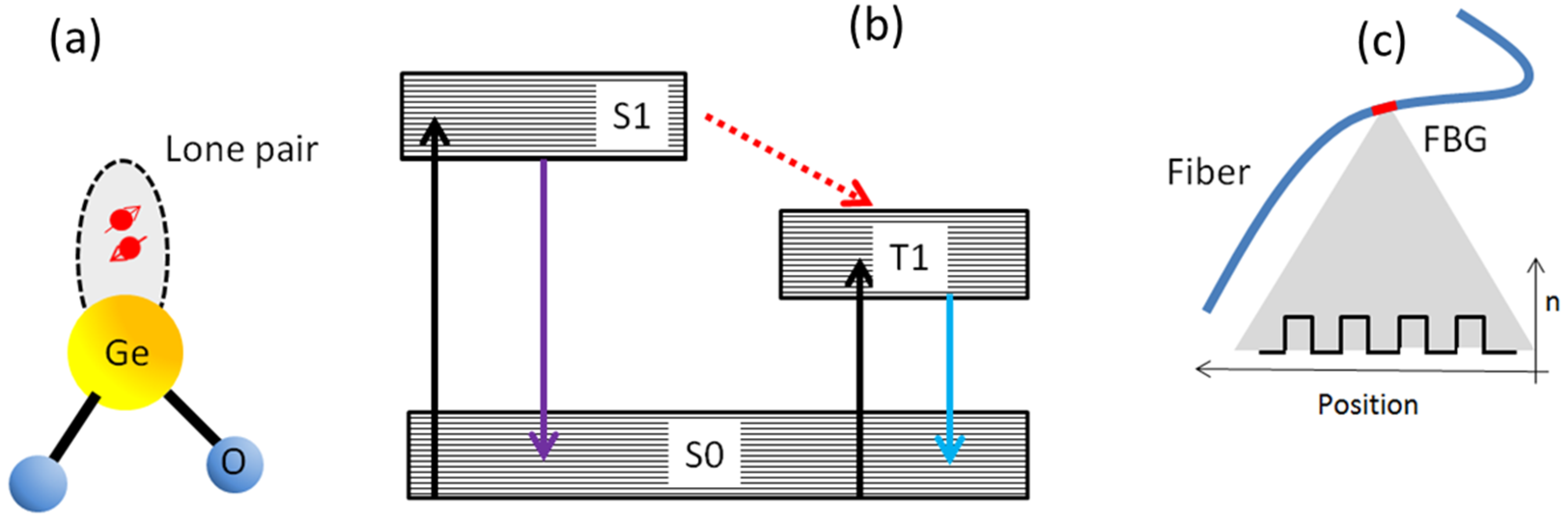
The so-called GLPC (germanium lone pair center) or two-fold coordinated germanium [75,76] is a useful example of a defect that is generated during preform and drawing processes in Ge-doped silica for fibers [65,72,73,74]. This defect has been used for the understanding of basic physical aspects, and its presence can be an advantage or a disadvantage in silica-based devices. For clarity, we remind of the accepted structural model and the optical properties of such a defect, which should be considered as almost definitive. The defect, as suggested by its name and as illustrated in Figure 3a, is constituted by a Ge atom linked by two single bonds with two O atoms and having a lone pair of electrons [72,75,76]. It is well accepted that it is responsible for an absorption band at about 5.15 eV (singlet–singlet allowed transition) and for another band at about 3.8 eV (singlet–triplet forbidden transition). Furthermore, the GLPC is a luminescent defect with bands at 4.3 eV (singlet–singlet transition) and 3.2 eV (triplet–singlet transition) [72,76]. The GLPC energy levels scheme is illustrated in Figure 3b. In Ge-doped silica, its easy formation has been studied and published in [72,77].
As reported in [65,73,74], Ge-doped silica preforms are usually rich in GLPC, especially in the central part of the Ge-doped region. Although the specific details of the formation mechanisms of this defect can require significant effort, it is not difficult to justify its high generation. For many years, and in some cases also today, maintaining the correct refractive index profile in the central core requires high production skills and competence. Such difficulties are related to the collapsing phase required by many of the production techniques. During this phase, the central core undergoes high stresses, which can lead to dopant profile modifications and/or a decrease of oxygen content [65,71,78,79]. The concentration of GLPC continues to increase during the fiber-drawing phase [73,74].
The relevance of GLPC in silica has been proven at different levels and for different applications. There are two main reasons: (i) this defect is an electron donor [74,80,81,82] and (ii) its absorption is at about 5 eV. It is clear that the presence of an electron donor tends to increase the radiation sensitivity of the material to X- or γ-rays or to lasers with wavelengths within its absorption bands. It has been proven that a Ge-doped fiber is more radiation-sensitive than its original preform [74,83] because of the GLPC formation during the drawing. The GLPC content increases the generation of defects absorbing in the UV with tails in the visible spectral range; for this and other reasons, Ge-doped fibers are not radiation resistant in this spectral range [9,64,80,81,82,83,84,85]. At the same time, the presence of GLPC and the associated photosensitivity can be used as an advantage. This is the case of the inscription of FBG (for temperature and strain point sensors production) in Ge-doped silica with UV laser [6,25,86,87]. Figure 3c illustrates the periodic structure of the refractive index in a FBG.
In basic research, GLPC has also been a relevant investigation tool. In combination with defects having similar structures, but in which either Si or Sn takes the place of Ge, it was possible to clarify the nature of the absorption at 5 eV and of the emissions excited at this energy in silica [75,76]. The study was also supported by the fact that under irradiation, these defects are transformed into other paramagnetic ones, such as H (I, II, III) [6,76,77]. This kind of investigation is a perfect example of how the combination of the study of optical and paramagnetic properties and irradiation effects is able to improve the knowledge of a material [76,77].
The presence of GLPC was used to evidence multiphoton absorption in silica [88]. As a consequence of this effect and in some cases of the band gap decrease related to the Ge doping, it is worth noting that in GLPC-rich samples, nanoparticles were produced with a UV ns-pulsed laser at fluences lower than those required for pure silica [89,90]. The presence of an absorption band at about 5 eV and the Ge doping are the key factors for the material´s energy absorption from the laser, allowing nanoparticle production, the generation of defects, structural modifications, and the possibility of FBG inscription with a UV laser [6,86,87,89,90].
In the context of defect generation, the study of mechanisms induced by irradiation represents a large part of the scientific literature, where application-driven and basic research points of view have been used.
Irradiation with X-, γ-rays, laser, neutrons, electrons, or fast ions is a well-known source of the modification of the proprieties of any material. It is useful to underline that for bulk silica (lens or mirrors) and optical fibers, the effects can be studied in terms of the total ionizing dose (TID). For microelectronic devices, this is not sufficient, and a large part of the investigation regards the single-event effects (SEE) [1,2,3,4].
Due to the widespread application of microelectronics and optoelectronics devices in radiation environments, such as space, nuclear reactors, nuclear waste repositories, ITER, LMJ, accelerators (such as CERN or DESY), there is a vast body of literature focused on the investigation of the radiation effects in silica-containing devices. The interest is also increased with the production of optical fiber-based sensors, which can be employed even under harsh conditions in which microelectronics fail [7,8,9]. All environments in which these devices are used differ for the total accumulated dose during operation, dose rate, temperature, and other external conditions [7]. Furthermore, such parameters can also change with time within the same environments. The dose rate and temperature are not constant during a space mission; in large installations such as CERN, the dose rate also depends on the position with respect to the sources of radiation and accelerator operations.
At the same time, the mechanisms of generation of defects involve several steps in which diffusion, trapping, and recombination processes can be present [6,12]. These make the radiation response of silica dependent on the temperature (T), dose rate, atmosphere, and probing conditions [1,7,8,69,84,91]. In the field of optical fibers, the destruction or recombination of defects as a consequence of thermally activated processes is named thermal bleaching; the one resulting from light is referred to as photobleaching, whereas the generation of defects from light absorption is called photodarkening.
Since diffusion coefficients are temperature dependent [92], the presence of diffusion processes in the path that goes from the first interaction of radiation with the silica to the defect formation introduces the T dependence on the radiation response. At the same time, charge or atoms trapping or de-trapping processes are also T-dependent. An example of the T dependence of the point defect generation can be seen on the non-monotone behavior of the RIA induced in some pure silica optical fibers [93], which is mainly attributable to the temperature dependence of E’Si and NBOHC defects generation and stability on T. Regarding the dose rate dependence, the following considerations should be made. Firstly, the defect generation, back-conversion, or conversion processes are photoinduced so that their rates are, in principle, dose rate-dependent. Furthermore, at any temperature, the presence of diffusion or trapping/de-trapping processes can imply additional dependences on time and therefore on the dose rate, because all these processes have their specific rate and because the number of events depends on time. Therefore, changing the dose rate and, as a consequence, the time needed to reach a certain dose, the amount of the detected defect can change.
All the applications involving optical fibers comprise the presence of light traveling in the fiber itself. This light can be absorbed by some defects in the fibers. When this happens, the defects are in an excited state, and they return to the ground state by emitting light or transferring energy to the matrix [6]. Due to the coupling of the defects with the matrix, the de-excitation path almost always involves the transfer of a part of the energy to the matrix [6]. This implies an increase of T, which, in principle, impacts the defect generation/conversion itself. Light absorption can also enhance the charge de-trapping or can induce molecular destruction when the excited state is an anti-bonding state. Then, these phenomena can be followed by the diffusion of the charge or of the resulting atoms to other sites where they can form different point defects. Figure 4a illustrates two electron traps having different stability as a consequence of the different depth of the potential well, whereas Figure 4b shows a molecule having an excited state non-bonding or anti-bonding level, in which the molecule can be found as a consequence of light absorption, and that can cause its dissociation.
Something that should always be considered in studying radiation effects is that if one of the parameters mentioned above is changed, the details of the microscopic radiation-induced processes can change too, with a consequent variation of the impact of the other irradiation parameters. For example, decreasing the temperature decreases the impact of the thermal bleaching, but the defects not destroyed by thermal bleaching can be much more sensitive to photobleaching.
4. E´ Defects, a Famous Member of the Silica’s Saga
One of the most studied defects in silica is the Si-E´γ defect. Such a defect is constituted by a threefold coordinated Si atom with an unpaired electron, and so it is paramagnetic [6,12,32,98,99,100,101,102,103,104,105,106,107,108]. After decades of investigations, many properties of this defect, its generation, and relation with the network are known [6,12,32,98,99,100,101,102,103,104,105,106]. The presence and formation under irradiation of the Si-E´ in the SiO2 layers and in the Si/SiO2 interface of components has been recognized as crucial in microelectronics [1,2,3,4,106]. Beyond this, the present section is more focused on how much this defect was and can be used to improve the understanding of various aspects of silica and radiation-induced processes. For the clarity of the following, it is also important to remind that the 29Si has a natural abundance of about 4.67% and that, differing from the 28Si, it has a nuclear magnetic momentum of quantum number ½ [6,12,101,102,103,104,105]. Consequently, the Si-E´γ presents a hyperfine doublet of lines in the EPR spectra with separation of about 420 Gauss (42 mT) [101,102,103,104,105]. This feature is particularly relevant, and Devine et al. [6,103,104] have demonstrated that the separation between the two lines depends on the density of the silica, even under irradiation, where a maximum of about 4% of densification is observed. Thanks to such relation between the hyperfine lines separation and the silica density, it is possible to improve the knowledge on defects generation and on the matrix modification, which imply refractive index changes [12,25].
For example, it is known that densification under photon irradiation differs from that one observed under swift ions irradiation [105]. A possible explanation of this difference was reported by Buscarino et al. in [105] studying the behavior of Si-E´γ hyperfine doublet signal. Similarly, the hyperfine lines separation was used to investigate the structure of the inner part of the silica nanoparticles both with respect to the bulk silica and as a function of the nanoparticles’ sizes [35]. One of the main results of this study was to support the core shell model for silica nanoparticles in which the core and the surface shell structures are different and independent from the nanoparticles’ size [30,33,34,35,36,37,38,39,40].
In the context of the E’-like defects family, it is interesting to note that several widely used dopants give rise to defects with E’-like structures [6,9,100,101,102,108], so in principle, their EPR hyperfine lines should have a dependence on the density. This feature could be mapped and used to investigate the density and the radiation effects in different parts of an optical fiber with quite high precision. The density and hyperfine line separation correlation of such signals should be obviously established before.
5. Advantages and Disadvantages of the Radiation-Induced Attenuation
Optical fiber manufacturing implies the production of glass with refractive index profiles, which allow the guiding of light in the core. There are various ways of achieving this. Obviously, the doping of core or cladding to increase or decrease the refractive index is the most common. Doping has not only the role of modifying the refractive index, but it can also modify other optical features of the silica, and it is used to produce specific fibers for different applications [6,7,8,9,10,11,12]. Many chemical elements have been used to dope silica, from sensor applications to laser or amplifier manufacturing [6,7,8,9]. As a result of the doping, specific dopant-related defects are introduced in the material [6,7,8,9]. The presence of such point defects makes the response of any type of fiber a specific field of investigation. So while pure silica, F-doped, and N-doped fibers are relevant in temperature and strain sensors in harsh environments, Al and P-doped fibers are promising candidates as dosimeters [9,109,110,111,112,113,114,115,116,117,118]. In the first case, the radiation hardness is fundamental, since low RIA gives the opportunity for long-range transmission and to produce point or distributed sensors, eventually with large sensing ranges. On the other hand, the radiation sensitivity, dose rate, and temperature independence of the RIA are needed for dosimetry applications and are fundamental for the second family of fibers. In other words, the same basic process, but related to different defects, represents a limit or an advantage. In the case of temperature and strain sensors, the RIA level and the detection limit impose the lengths of the fiber that can be employed. In dosimetry or radiation detection, obviously, the detection of the signal is still fundamental, but other aspects have to be considered. The low-dose detection imposes high radiation sensitivity, while the independences from dose rate, temperature, and history are also needed, since the increase of the RIA as a function of the dose is used to monitor the radiation environments [113,114,115,116,117,118].
Raman-based temperature sensors represent an example of devices where the RIA can generate problems [109,112].
In Raman scattering, the ratio between the Stokes and anti-Stokes lines intensity, which was observed respectively at higher and shorter wavelengths with respect to the excitation light (typically a laser line), is related to the temperature. This can be used as a temperature-distributed sensor using an OTDR (optical time domain reflectometry) with opportune calibration procedures [109,112]. Figure 5a and its caption briefly describe the operation configuration of OTDR.
When these sensors have to operate in radiation environments, RIA not only affects the maximum length of usable fiber, but it can be a source of error in the T monitoring even when the signal is transmitted. For example, a single-ended sensor equipped with a single laser excitation can incur other problems. For this kind of device, the main problem is the RIA dependence on the wavelength (differential RIA) [109]. As a consequence, the amplitude of the anti-Stokes and Stokes signals is reduced differently, so the ratio is no longer related to the T [109].
A design solution to this problem is constituted by the use of two excitation probe lasers [112]. In these systems, the monitored Stokes signal is the one excited by the shorter wavelength laser and centered at the wavelength of the second excitation probe [112]. In contrast, the monitored anti-Stokes signal is the one generated by the longer wavelength laser and located at the wavelength of the shorter one [112]. As a consequence of this, the RIA dependence on the wavelength is no more a problem when the RIA changes are small during the data recording. Indeed, due to the spectral overlap of each Raman signal with the excitation laser of the other signal, the acquired amplitudes are similarly affected by the RIA at both the employed wavelengths (according to Lambert–Beer law). Anyway, since the two probing laser pulses are injected at different times, the ratio between Stokes and anti-Stokes lines gives a good T estimation when the RIA changes are slow with time [112]. Monitoring the Rayleigh scattering at the two wavelengths is also a good choice to monitor the RIA at the same time.
In general, while RIA is a disadvantage for optical fiber technology, a clear example in which it can be used as an advantage is represented by Al and P-doped fibers [113,117]. This latter kind of fiber can be used as a distributed dosimeter or radiation detection employing OTDR technology and taking advantage from the Rayleigh scattering. The performances of such sensors are based on the spatial resolution of the OTDR and on the optical properties of P or Al-related point defects and on their generation processes under irradiation. In the case of the P-doped fibers, it is known that the P1 defects (belonging to the E’ family) absorb at 1550 nm [108]; various investigations have shown that is possible to use such fiber for radiation detection and dosimetry [113,114,116,118]. Indeed, the fibers are radiation sensitive, the RIA is stable after the end of the irradiation, and it does not feature strong or limiting dependence on the dose rate and temperature, allowing their use in radiation environments such as CERN and DESY [113,114,116,118]. Figure 5b illustrates how an OTDR trace appears when different parts of a fiber absorbed different doses. Al-doped fibers represent a different case; these fibers are more radiation sensitive, but the RIA features a certain amount of recovery [117] that has to be considered for applications. Furthermore, the specific defects that originate the RIA in the near infrared domain, where the sensor should operate, are still unknown [9,119].
In Table 1, we summarize the main defects that have been treated in the manuscript, reporting their positive or negative impacts on the silica properties considering applications. It is worth noting that the same aspect can be in both columns just because of a different application. For the strained bonds and especially for defect absorbing in the near-infrared (NIR), we just report a possible positive use of their presence, while the improvement of their understanding is required to be more specific. In the last column, we indicate the main process that implies the defects’ generation.
6. Conclusions
For many decades, point defects in silica have been studied both for their impact on the macroscopic properties of silica and for their impact on silica-based microelectronic and optoelectronic devices. Many examples of the long and difficult path needed to identify the generation, optical, electric, and structural properties of each species can be found in the literature. Further decades of years should and will be devoted to this field of research because despite all these efforts, many questions are still open as a consequence of the complexity of the topic and of the continuous increase of types of doping, co-doping, and applications. The knowledge acquired through the in-depth study of point defects can often be used to our advantage. High photosensitive materials, which are not used as temperature sensors or data transmission in radiation environments, could be used as dosimeter or for FBG production. The approach we want to promote is one in which a technical obstacle is turned into an asset. Furthermore, the knowledge relating to point defects and how they influence the final device can always be used to select, from the beginning, the production procedures of the materials according to the final device application.
Author Contributions
Writing—original draft preparation, A.A.; writing—review and editing, A.A., J.K., G.B., D.D.F., S.A.
Funding
This research received no external funding.
Acknowledgments
The authors want to thank the present and the former members of the LAMP group (http://www1.unipa.it/lamp/people.htm) at the University of Palermo, the MOPERE group at Laboratoire Hubert Curien, Univerite’ Jean Monnet, Saint Etienne, and the NEO unit at Fraunhofer Institute for Technological Trend Analysis INT (https://www.int.fraunhofer.de/en/business_units/nuclear_effects_inelectronicsandoptics.html) for useful discussions during the last years, which are the basis of this paper.
Conflicts of Interest
The authors declare no conflict of interest.
References
- Schwank, J.R.; Shaneyfelt, M.R.; Fleetwood, D.M.; Felix, J.A.; Dodd, P.E.; Paillet, P.; Ferlet-Cavrois, V. Radiation Effects in MOS Oxide. IEEE Trans. Nucl. Sci. 2008, 55, 1833–1853. [Google Scholar] [CrossRef]
- Schwank, J.R.; Ferlet-Cavrois, V.; Shaneyfelt, M.R.; Paillet, P.; Dodd, P.E. Radiation Effects in SOI Technologies. IEEE Trans. Nucl. Sci. 2003, 50, 522–537. [Google Scholar] [CrossRef]
- Paillet, P. Overview of the Main Concepts of Radiation Effects and Their Evolution over the 30 Years of RADECS Conferences. In Proceedings of the Radiation and its Effects on Components and Systems, Montpellier, France, 16–20 September 2019. [Google Scholar]
- Fleetwood, D. TID Effects, Border Traps, and 1/f Noise in Emerging Technologies. In Proceedings of the Radiation and its Effects on Components and Systems, Montpellier, France, 16–20 September 2019. [Google Scholar]
- Paleari, A.; Meinardi, F.; Brovelli, S.; Lorenzi, R. Competition between green self-trapped-exciton and red non-bridging-oxygen emissions in SiO2 under interband excitation. Commun. Phys. 2018, 1, 67. [Google Scholar] [CrossRef]
- Pacchioni, G.; Skuja, L.; Griscom, D.L. Defects in SiO2 and Related Dielectrics: Science and Technology; Kluwer Academic: Dordrecht, The Netherlands, 2000. [Google Scholar]
- Girard, S.; Kuhnhenn, J.; Gusarov, A.; Brichard, B.; Van Uffelen, M.; Ouerdane, Y.; Boukenter, A.; Marcandella, C. Radiation Effects on Silica-Based Optical Fibers: Recent Advances and Future Challenges. IEEE Trans. Nucl. Sci. 2013, 60, 2015–2036. [Google Scholar] [CrossRef]
- Girard, S.; Morana, A.; Ladaci, A.; Robin, T.; Mescia, L.; Bonnefois, J.-J.; Boutillier, M.; Mekki, J.; Paveau, A.; Cadier, B.; et al. Recent advances in radiation-hardened fiber-based technologies for space applications. J. Opt. 2018, 20, 093001. [Google Scholar] [CrossRef]
- Girard, S.; Alessi, A.; Richard, N.; Martin-Samos, L.; De Michele, V.; Giacomazzi, L.; Agnello, S.; Di Francesca, D.; Morana, A.; Winkler, B.; et al. Overview of radiation induced point defects in silica-based optical fibers. Rev. Phys. 2019, 4, 100032. [Google Scholar] [CrossRef]
- Dragic, P.D.; Cavillon, M. Ballato Materials for optical fiber lasers: A review. J. Appl. Phys. Rev. 2018, 5, 041301. [Google Scholar] [CrossRef]
- Girard, S.; Allanche, T.; Paillet, P.; Goiffon, V.; Van Uffelen, M.; Mont-Casellas, L.; Muller, C.; Boukenter, A.; Ouerdane, Y.; De Cock, W. Growth and Decay Kinetics of Radiation-Induced Attenuation in Bulk Optical Materials. IEEE Trans. Nucl. Sci. 2018, 65, 1612–1618. [Google Scholar] [CrossRef]
- Devine, R.A.B.; Duraud, J.P.; Dooryhée, E. Structure and Imperfections in Amorphous and Crystalline Silicon Dioxide; Wiley: New York, NY, USA, 2000. [Google Scholar]
- Singh, L.P.; Bhattacharyya, S.K.; Kumar, R.; Mishra, G.; Sharma, U.; Singh, G.; Ahalawat, S. Sol-Gel processing of silica nanoparticles and their applications. Adv. Colloid Interface Sci. 2014, 214, 17–37. [Google Scholar] [CrossRef]
- Schärtl, W. Current directions in core–shell nanoparticle design. Nanoscale 2010, 2, 829–843. [Google Scholar]
- Davies, G.L.; McCarthy, J.E.; Rakovich, A.; Gun’ko, Y.K. Towards white luminophores: Developing luminescent silica on the nanoscale. J. Mater. Chem. 2012, 22, 7358–7365. [Google Scholar] [CrossRef]
- Li, L.; Wang, W.; Tang, J.; Wang, Y.; Liu, J.; Huang, L.; Wang, Y.; Guo, F.; Wang, J.; Shen, W.; et al. Classification, Synthesis, and Application of Luminescent Silica Nanoparticles: A Review. Nanoscale Res. Lett. 2019, 14, 190. [Google Scholar] [CrossRef] [PubMed]
- Alessi, A.; Girard, S.; Cannas, M.; Agnello, S.; Boukenter, A.; Ouerdane, Y. Influence of Drawing Conditions on the Properties and Radiation Sensitivities of Pure-Silica-Core Optical Fibers. J. Lightwave Technol. 2012, 30, 1726–1732. [Google Scholar] [CrossRef]
- Imai, H.; Arai, K.; Isoya, J.; Hosono, H.; Abe, Y.; Imagawa, H. Generation of centers and oxygen hole centers in synthetic silica glasses by y irradiation. Phys. Rev. B 1993, 48, 3116–3123. [Google Scholar] [CrossRef] [PubMed]
- Griscom, D.L. Fractal kinetics of radiation-induced point-defect formation and decay in amorphous insulators: Application to color centers in silica-based optical fibers. Phys. Rev. B 2001, 64, 174201. [Google Scholar] [CrossRef]
- Arai, K.; Imai, H.; Isoya, J.; Hosono, H.; Abe, Y.; Imagawa, H. Evidence for pair generation of an E’ center and a nonbridging oxygen-hole center in γ-ray-irradiated fluorine-doped low-OH synthetic silica glasses. Phys. Rev. B 1992, 45, 10818. [Google Scholar] [CrossRef]
- Griscom, D.L. Self-trapped holes in pure-silica glass: A history of their discovery and characterization and an example of their critical significance to industry. J. Non-Cryst. Solids 2006, 352, 2601–2617. [Google Scholar] [CrossRef]
- El-Sayed, A.-M.; Tanimura, K.; Shluger, A.L. Optical signatures of intrinsic electron localization in amorphous SiO2. J. Phys. Condens. Matter 2015, 27, 265501. [Google Scholar] [CrossRef]
- El-Sayed, A.-M.; Watkins, M.B.; Afanas’ev, V.V.; Shluger, A.L. Nature of intrinsic and extrinsic electron trapping in SiO2. Phys. Rev. B 2014, 89, 125201. [Google Scholar] [CrossRef]
- Tomashuk, A. Inherent and Strain-Assisted Radiation-Induced Self-Trapped Holes in Pure-Silica Optical Fibers. Adv. Photonics 2018. [Google Scholar] [CrossRef]
- Gusarov, A.; Hoeffgen, S.K. Radiation Effects on Fiber Gratings. IEEE Trans. Nucl. Sci. 2013, 60, 2037–2053. [Google Scholar] [CrossRef]
- Pissadakis, S. Laser processing of optical fibers: New photosensitivity findings, refractive index engineering and surface structuting. In Laser Growth and Processing of Photonic Devices; Vainos, N.A., Ed.; Woodhead Publishing Limited: Cambridge, UK, 2012; pp. 374–452. [Google Scholar]
- Agrawal, G.P. Fiber-Optic Communication Systems, 3rd ed.; John Wiley and Sons Inc.: New York, NY, USA, 2002. [Google Scholar]
- Rimola, A.; Costa, D.; Sodupe, M.; Lambert, J.; Ugliengo, P. Silica Surface Features and Their Role in the Adsorption of Biomolecules: Computational Modeling and Experiments. Chem. Rev. 2013, 113, 4216−4313. [Google Scholar] [CrossRef] [PubMed]
- Ghasemnejad, M.; Ahmadi, E.; Mohamadnia, Z.; Doustgani, A.; Hashemikia, S. Functionalized silica nanoparticles as a carrier for Betamethasone Sodium Phosphate: Drug release study and statistical optimization of drug loading by response surface method. Mater. Sci. Eng. C 2015, 56, 223–232. [Google Scholar] [CrossRef] [PubMed]
- Roder, A.; Kob, W.; Binder, K. Structure and dynamics of amorphous silica surfaces. J. Chem. Phys. 2001, 114, 7602–7614. [Google Scholar] [CrossRef]
- Uchino, T.; Aboshi, A.; Kohara, S.; Ohishi, Y.; Sakashita, M.; Aoki, K. Microscopic structure of nanometer-sized silica particles. Phys. Rev. B 2004, 69, 155409. [Google Scholar] [CrossRef]
- Stesmans, A.; Clémer, K.; Afanas’ev, V.V. Electron spin resonance probing of fundamental point defects in nanometer-sized silica particles. Phys. Rev. B 2005, 72, 155335. [Google Scholar] [CrossRef]
- Alessi, A.; Iovino, G.; Buscarino, G.; Agnello, S.; Gelardi, F.M. Entrapping of O2 Molecules in Nanostructured Silica Probed by Photoluminescence. J. Phys. Chem. C 2013, 117, 2616–2622. [Google Scholar] [CrossRef]
- Agnello, S.; Di Francesca, D.; Alessi, A.; Iovino, G.; Cannas, M.; Girard, S.; Boukenter, A.; Ouerdane, Y. Interstitial O2 distribution in amorphous SiO2 nanoparticles determined by Raman and photoluminescence spectroscopy. J. Appl. Phys. 2013, 114, 104305. [Google Scholar] [CrossRef]
- Alessi, A.; Agnello, S.; Buscarino, G.; Boizot, B.; Cannas, M.; Gelardi, F.M. Silica nanoparticle core structure examined by the E′Siγ center 29Si strong hyperfine interaction. J. Non-Cryst. Solids 2015, 423–424, 41–44. [Google Scholar] [CrossRef]
- Vaccaro, G.; Buscarino, G.; Agnello, S.; Sporea, A.; Oproiu, C.; Sporea, D.G.; Gelardi, F.M. Structure of Amorphous SiO2 Nanoparticles Probed through the E′γ Centers. J. Phys. Chem. C 2012, 116, 144–149. [Google Scholar] [CrossRef]
- Alessi, A.; Agnello, S.; Buscarino, G.; Gelardi, F.M. Structural properties of core and surface of silica nanoparticles investigated by Raman spectroscopy. J. Raman Spectrosc. 2013, 44, 810–816. [Google Scholar] [CrossRef]
- Alessi, A.; Agnello, S.; Buscarino, G.; Boizot, B.; Cannas, M.; Gelardi, F.M. β-ray irradiation effects on silica nanoparticles. IOP Conf. Ser. Mater. Sci. Eng. 2015, 80, 012011. [Google Scholar] [CrossRef]
- Vaccaro, L.; Spallino, L.; Agnello, S.; Buscarino, G.; Cannas, M. Defect-related visible luminescence of silica nanoparticles. Phys. Status Solidi C 2013, 10, 658–661. [Google Scholar] [CrossRef] [Green Version]
- Glinka, Y.D.; Lin, S.H.; Chen, Y.T. Time-resolved photoluminescence study of silica nanoparticles as compared to bulk type-III fused silica. Phys. Rev. B 2002, 66, 035404. [Google Scholar] [CrossRef]
- Vaccaro, G.; Agnello, S.; Buscarino, G.; Cannas, M.; Vaccaro, L. Structural and luminescence properties of amorphous SiO2 nanoparticles. J. Non-Cryst. Solids 2011, 357, 1941–1944. [Google Scholar] [CrossRef]
- Lemaire, P.J.; Atkins, R.M.; Mizrahi, V.; Reed, W.A. High pressure H2 loading as a technique for achieving ultra-high UV photosensitivity and thermal sensitivity in GeO2 doped optical fibres. Electron. Lett. 1993, 29, 1191–1193. [Google Scholar] [CrossRef]
- Henschel, H.; Hoeffgen, S.K.; Kuhnhenn, J.; Weinand, U. Influence of manufacturing parameters and temperature on the radiation sensitivity of fiber Bragg gratings. IEEE Trans. Nucl. Sci. 2010, 57, 2029–2034. [Google Scholar] [CrossRef]
- Klein, K.-F.; Khalilov, V.K. UV-fibers: Two decades of improvement for new applications. Proc. SPIE 2015, 9317, 93170S. [Google Scholar]
- Brichard, B.; Tomashuk, A.L.; Bogatyrjov, V.A.; Fernandez, A.F.; Klyamkin, S.N.; Girard, S.; Berghmans, F. Reduction of the radiation-induced absorption in hydrogenated pure silica core fibres irradiated in situ with γ-rays. J. Non-Cryst. Solids 2007, 353, 466–472. [Google Scholar] [CrossRef]
- Griscom, D.L. Thermal bleaching of x-ray-induced defect centers in high purity fused silica by diffusion of radiolytic molecular hydrogen. J. Non-Cryst. Solids 1984, 68, 301–325. [Google Scholar] [CrossRef]
- Brichard, B.; Fernandez Fernandez, A.; Ooms, H.; Berghmans, F.; Decreton, M.; Tomashuk, A.; Klyamkin, S.; Zabezhailov, M.; Nikolin, I.; Bogatyrjov, V.; et al. Radiation-hardening techniques of dedicated optical fibres used in plasma diagnostic systems in ITER. J. Nucl. Mater. 2004, 329–333, 1456–1460. [Google Scholar] [CrossRef]
- Nagasava, K.; Hoshi, Y.; Ohki, Y.; Yahagi, K. Improvement of radiation resistance of pure silica core fibers by hydrogen treatment. Jpn. J. Appl. Phys. 1985, 24, 1224–1228. [Google Scholar] [CrossRef]
- Messina, F.; Cannas, M.; Boscaino, R. Influence of hydrogen on paramagnetic defects induced by UV laser exposure in natural silica. Phys. Stat. Sol. C 2005, 2, 616–619. [Google Scholar] [CrossRef] [Green Version]
- Lopez, N.; Vitiello, M.; Illas, F.; Pacchioni, G. Interaction of H2 with strained rings at the silica surface from ab initio calculations. J. Non-Cryst. Solids 2000, 271, 56–63. [Google Scholar] [CrossRef]
- Skuja, L.; Kajihara, K.; Hirano, M.; Hosono, H. Visible to vacuum-UV range optical absorption of oxygen dangling bonds in amorphous SiO2. Phys. Rev. B 2011, 84, 205206. [Google Scholar] [CrossRef]
- Skuja, L. Time-Resolved low temperature Luminescence of non-bridging oxygen hole centers in silica glass. Solid State Commun. 1992, 84, 613–616. [Google Scholar] [CrossRef]
- Cannas, M.; Gelardi, F.M. Vacuum ultraviolet excitation of the 1.9-eV emission band related to nonbridging oxygen hole centers in silica. Phys. Rev. B 2004, 69, 153201. [Google Scholar] [CrossRef]
- Brinker, C.J. Hydrolysis and condensation of silicates: Effects on structure. J. Non-Cryst. Solids 1988, 100, 31–50. [Google Scholar] [CrossRef] [Green Version]
- Kajihara, K. Recent advances in sol–gel synthesis of monolithic silica and silica-based glasses. J. Asian Ceram. Soc. 2013, 1, 121–133. [Google Scholar] [CrossRef] [Green Version]
- Alessi, A.; Girard, S.; Marcandella, C.; Vaccaro, L.; Cannas, M.; Boukenter, A.; Ouerdane, Y. Influence of the Manufacturing Process on the Radiation Sensitivity of Fluorine-Doped Silica-Based Optical Fibers. IEEE Trans. Nucl. Sci. 2012, 59, 760–766. [Google Scholar] [CrossRef]
- Griscom, D.L.; Friebele, E.J.; Mukherjee, S.P. Studies of radiation- induced point defects in silica aerogel monoliths. Cryst. Latt. Def. Amorph. Mater. 1987, 17, 157–163. [Google Scholar]
- Griscom, D.L. Optical absorption of—Hole type centers in irradiated alkali halide-alkali borate glasses. J. Chem. Phys. 1969, 51, 5186–5187. [Google Scholar] [CrossRef]
- Griscom, D.L.; Friebele, J. Fundamental radiation-induced defects centers in synthetic fused silica: Atomic chlorine, delocalizated e’centers, and triplet state. Phys. Rev. B 1986, 34, 7524–7533. [Google Scholar] [CrossRef] [PubMed]
- Skuja, L.; Kajihara, K.; Smits, K.; Silins, A.; Hosono, H. Luminescence and Raman Detection of Molecular Cl2 and ClClO Molecules in Amorphous SiO2 Matrix. J. Phys. Chem. C 2017, 121, 5261–5266. [Google Scholar] [CrossRef]
- Girard, S.; Marcandella, C.; Alessi, A.; Boukenter, A.; Ouerdane, Y.; Richard, N.; Paillet, P.; Gaillardin, M.; Raine, M. Transient Radiation Responses of Optical Fibers: Influence of MCVD Process Parameters. IEEE Trans. Nucl. Sci. 2012, 59, 2894–2901. [Google Scholar] [CrossRef] [Green Version]
- Dutton, H.J.R. Understanding Optical Communications, International Technical Support Organization. Available online: http://www.redbooks.ibm.com 1998 (accessed on 9 October 2019).
- Li, T. Optical Fiber Communications: Fiber Fabrication; Academic Press Inc.: Orlando, FL, USA, 1995; Volume 1. [Google Scholar]
- Di Francesca, D.; Boukenter, A.; Agnello, S.; Girard, S.; Alessi, A.; Paillet, P.; Marcandella, C.; Richard, N.; Gelardi, F.M.; Ouerdane, Y. X-ray irradiation effects on fluorine-doped germanosilicate optical fibers. Opt. Mat. Exp. 2014, 4, 1683–1695. [Google Scholar] [CrossRef]
- Atkins, G.R.; Sceats, M.G.; Poole, S.B.; Simmons, H.W. Profiling of drawing induced defects in optical fibre preforms. Elec. Lett. 1992, 28, 768–769. [Google Scholar] [CrossRef]
- Girard, S.; Trenteseaux, I.; Ouerdane, Y.; Meunier, J.-P.; Boukenter, A.; Derep, J.-L.; Thonnérieux, L. Radial distribution of attenuation in gamma irradiated single-mode optical fibers. Appl. Phys. Lett. 2003, 83, 219. [Google Scholar] [CrossRef]
- Lancry, M.; Ollier, N.; Babu, B.H.; Herrero, C.; Poumellec, B. EPR reversible signature of self-trapped holes in fictive temperature-treated silica glass. J. Appl. Phys. 2018, 123, 113101. [Google Scholar] [CrossRef]
- Friebele, E.J.; Sigel, G.H.; Griscom, D.L. Drawing-induced defect centers in a fused silica core fiber. Appl. Phys. Lett. 1976, 28, 516–518. [Google Scholar] [CrossRef]
- Kashaykin, P.F.; Tomashuk, A.L.; Salgansky, M.Y.; Guryanov, A.N.; Dianov, E.M. Anomalies and peculiarities of radiationinduced light absorption in pure silica optical fibers at different temperatures. J. Appl. Phys. 2017, 121, 213104. [Google Scholar] [CrossRef]
- Li, J.; Kannan, S.; Lehman, R.L.; Sigel, G.H. Drawing-enhanced defect precursors in low-OH content, oxygen-deficient synthetic silica optical fibers. Appl. Phys. Lett. 1994, 64, 2090. [Google Scholar] [CrossRef]
- Hanafusa, H.; Hibino, Y.; Yamamoto, F. Thermodynamical behavior of E’ center in the optical-fiber drawing process. Phys. Rev. B 1987, 35, 7646–7651. [Google Scholar] [CrossRef] [PubMed]
- Giacomazzi, L.; Martin-Samos, L.; Boukenter, A.; Ouerdane, Y.; Girard, S.; Alessi, A.; de Gironcoli, S.; Richard, N. Photoactivated processes in optical fibers: Generation and conversion mechanisms of twofold coordinated Si and Ge atoms. Nanotechnology 2017, 28, 195202. [Google Scholar] [CrossRef] [PubMed]
- Origlio, G.; Cannas, M.; Girard, S.; Boscaino, R.; Boukenter, A.; Ouerdane, Y. Influence of the drawing process on the defect generation in multistep-index germanium-doped optical fibers. Opt. Lett. 2009, 34, 2282–2284. [Google Scholar] [CrossRef] [PubMed]
- Alessi, A.; Girard, S.; Cannas, M.; Agnello, S.; Boukenter, A.; Ouerdane, Y. Evolution of Photo-induced defects in Ge-doped fiber/preform: Influence of the drawing. Opt. Express 2011, 19, 11680–11690. [Google Scholar] [CrossRef] [PubMed] [Green Version]
- Awazu, K.; Kawazoe, H.; Yamane, M. Simultaneous generation of optical absorption bands 5.14 and 0.452 eV in 9SiO2:GeO2 glasses heated under H2 atmosphere. J. Appl. Phys. 1990, 68, 2713–2718. [Google Scholar] [CrossRef]
- Skuja, L. Isoelectronic series of twofold coordinated Si, Ge, and Sn atoms in glassy SiO2: A luminescence study. J. Non-Cryst. Sol. 1992, 149, 77–95. [Google Scholar] [CrossRef]
- Pacchioni, G.; Ferrario, R. Optical transitions and EPR properties of two-coordinated Si, Ge, Sn and related H(I), H(II), and H(III) centers in pure and doped silica from ab initio calculations. Phys. Rev. B 1998, 58, 6090–6096. [Google Scholar] [CrossRef]
- Origlio, G.; Messina, F.; Cannas, M.; Boscaino, R.; Girard, S.; Boukenter, A.; Ouerdane, Y. Optical properties of phosphorus-related point defects in silica fiber preforms. Phys. Rev. B 2009, 80, 205208. [Google Scholar] [CrossRef]
- Donalds, L. Critical Design Goals to Manufacture Optical Fiber Preforms, Fiber Design and Manufacturing—Blog Article 2018. Available online: https://focenter.com/critical-design-goals-to-manufacture-optical-fiber-preforms/ (accessed on 24 September 2019).
- Griscom, D.L. On the natures of radiation-induced point defects in GeO2-SiO2 glasses: Reevaluation of a 26-year-old ESR and optical data set. Opt. Mat. Exp. 2011, 1, 400–412. [Google Scholar] [CrossRef]
- Fujimaki, M.; Kasahara, T.; Shimoto, S.; Miyazaki, N.; Tokuhiro, S.; Seol, K.S.; Ohki, Y. Structural changes induced by KrF excimer laser photons in H2-loaded Ge-doped SiO2 glass. Phys. Rev B 1999, 60, 4682–4687. [Google Scholar] [CrossRef]
- Alessi, A.; Girard, S.; Reghioua, I.; Fanetti, M.; Di Francesca, D.; Agnello, S.; Cannas, M.; Marcandella, C.; Martin-Samos, L.; Richard, N.; et al. Gamma and x-ray irradiation effects on different Ge and Ge/F doped optical fibers. J. Appl. Phys. 2015, 118, 085901. [Google Scholar] [CrossRef]
- Di Francesca, D.; Agnello, S.; Girard, S.; Alessi, A.; Marcandella, C.; Paillet, P.; Boukenter, A.; Gelardi, F.M.; Ouerdane, Y. O2-Loading Treatment of Ge-Doped Silica Fibers: Radiation Hardening Process. J. Lightwave Technol. 2016, 34, 2311–2316. [Google Scholar] [CrossRef]
- Alessi, A.; Di Francesca, D.; Girard, S.; Agnello, S.; Cannas, M.; Reghioua, I.; Martin-Samos, L.; Marcandella, C.; Richard, N.; Paillet, P.; et al. Irradiation Temperature Influence on the In Situ Measured Radiation Induced Attenuation of Ge-Doped Fibers. IEEE Trans. Nucl. Sci. 2016, 64, 2312–2317. [Google Scholar] [CrossRef]
- Neustruev, V.B. Colour centres in germanosilicate glass and optical fibres. J. Phys. Condens. Matter 1994, 6, 6901–6936. [Google Scholar] [CrossRef]
- Takahashi, M.; Uchino, T.; Yoko, T. Correlation between Macro- and Microstructural Changes in Ge:SiO2 and SiO2 Glasses under Intense Ultraviolet Irradiation. J. Am. Ceram. Soc. 2002, 85, 1089–1092. [Google Scholar] [CrossRef]
- Essid, M.; Albert, J.; Brebner, J.L.; Awazu, K. Correlation between oxygen-deffcient center concentration and KrF excimer laser induced defects in thermally annealed Ge-doped optical fiber preforms. J. Non-Cryst. Solids 1999, 246, 39–45. [Google Scholar] [CrossRef]
- Messina, F.; Cannas, M.; Boscaino, R. Generation of defects in amorphous SiO2 assisted by two-step absorption on impurity sites. J. Phys. Condens. Matter 2008, 20, 275210. [Google Scholar] [CrossRef]
- Reghioua, I.; Fanetti, M.; Girard, S.; Di Francesca, D.; Agnello, S.; Martin-Samos, L.; Cannas, M.; Valant, M.; Raine, M.; Gaillardin, M.; et al. Study of silica-based intrinsically emitting nanoparticles produced by an excimer laser Beilstein. J. Nanotechnol. 2019, 10, 211–221. [Google Scholar]
- Alessi, A.; Fanetti, M.; Agnello, S.; Girard, S.; Buscarino, G.; Di Francesca, D.; Reghioua, I.; Messina, F.; Cannas, M.; Martin-Samos, L.; et al. Ge-doped silica nanoparticles: Production and characterization. Opt. Mat. Exp. 2016, 6, 2213–2220. [Google Scholar] [CrossRef]
- Blanc, J.; Ricci, D.; Kuhnhenn, J.; Weinand, U.; Schumann, O.J. Irradiation of Radiation-Tolerant Single-Mode Optical Fibers at Cryogenic Temperature. J. Lightwave Technol. 2017, 35, 1929–1935. [Google Scholar] [CrossRef]
- Shewmon, P.G. Diusion in Solids; McGraw-Hill Book Company: New York, NY, USA, 1963. [Google Scholar]
- Girard, S.; Marcandella, C.; Morana, A.; Perisse, J.; Di Francesca, D.; Paillet, P.; Macé, J.-R.; Boukenter, A.; Léon, M.; Gaillardin, M.; et al. Combined High Dose and Temperature Radiation Effects on Multimode Silica-Based Optical Fibers. IEEE Trans. Nucl. Sci. 2013, 60, 4305–4313. [Google Scholar] [CrossRef]
- Alessi, A.; Agnello, S.; Girard, S.; Di Francesca, D.; Reghioua, I.; Marcandella, C.; Paillet, P.; Richard, N.; Martin-Samos, L.; Cannas, M.; et al. Coupled irradiation-temperature effects on induced point defects in germanosilicate optical fibers. J. Mater. Sci. 2017, 52, 10697–10708. [Google Scholar] [CrossRef]
- ESCC Basic Specification 22900, Total Dose Steady-state Irradiation Test Method. Available online: https://www.google.com/url?sa=t&rct=j&q=&esrc=s&source=web&cd=1&cad=rja&uact=8&ved=2ahUKEwjhlsiNoPjlAhUOb1AKHW9gA8MQFjAAegQIAxAC&url=http%3A%2F%2Fescies.org%2Fescc-specs%2Fpublished%2F22900.pdf&usg=AOvVaw1U6zF3GW_iS9uGeuGw7-1 (accessed on 9 October 2019).
- Mil-STD-750-1A Method 1019.5 Steady-state Total Dose Irradiation Procedure. Available online: https://www.google.com/url?sa=t&rct=j&q=&esrc=s&source=web&cd=1&cad=rja&uact=8&ved=2ahUKEwjhod32oPjlAhVRKVAKHb-CBMQQFjAAegQIARAC&url=https%3A%2F%2Fwww.atecorp.com%2FATECorp%2Fmedia%2FPDFs%2F750-1.pdf&usg=AOvVaw1i-GWORkfYyueAjJM84N1m (accessed on 9 October 2019).
- ESCC Basic Specification 25100, Single Event Effects Test Method and Gudelines. Available online: https://escies.org/webdocument/showArticle?id=229 (accessed on 9 October 2019).
- Weeks, R.A. Paramagnetic Resonance of Lattice Defects in Irradiated Quartz. J. Appl. Phys. 1956, 27, 1376–1381. [Google Scholar] [CrossRef]
- Weeks, R.A. The many varieties of E’ centers: A review. J. Non-Cryst. Solids 1994, 179, 1–9. [Google Scholar] [CrossRef]
- Weeks, R.A.; Magruder, R.H., III; Stesmans, A. Review of some experiments in the 50 year saga of the E′ center and suggestions for future research. J. Non-Cryst. Solids 2008, 354, 208–216. [Google Scholar] [CrossRef]
- Alessi, A.; Agnello, S.; Buscarino, G.; Pan, Y.; Mashkovtsev, R.I. EPR on Radiation-Induced Defects in SiO2. In Applications of EPR in Radiation Research; Lund, A., Shiotani, M., Eds.; Springer: Heidelberg, Germany, 2014; pp. 255–295. [Google Scholar]
- Griscom, D.L. Characterization of three E’-center variants in X- and γ-irradiated high purity a-SiO2. Nucl. Instrum. Methods Phys. Res. B 1984, 1, 481–488. [Google Scholar] [CrossRef]
- Devine, R.A.B.; Arndt, J. Si—O bond-length modification in pressure-densified amorphous SiO2. Phys. Rev. B 1987, 35, 9376–9379. [Google Scholar] [CrossRef]
- Douillard, L.; Jollet, F.; Duraud, J.P.; Devine, R.A.B.; Dooryhee, E. Radiation damage produced in quartz by energetic ions. Radiat. Eff. Defects Solids 1992, 124, 351–370. [Google Scholar] [CrossRef]
- Buscarino, G.; Agnello, S.; Gelardi, F.M.; Boscaino, R. Polyamorphic transformation induced by electron irradiation in a-SiO2 glass. Phys. Rev. B 2009, 80, 094202. [Google Scholar] [CrossRef]
- Pantelides, S.T.; Lu, Z.-Y.; Nicklaw, C.; Bakos, T.; Rashkeev, S.N.; Fleetwood, D.M.; Schrimpfc, R.D. The E′ center and oxygen vacancies in SiO2. J. Non-Cryst. Solids 2008, 354, 217–223. [Google Scholar] [CrossRef]
- Griscom, D.L. Trapped-electron centers in pure and doped glassy silica: A review and synthesis. J. Non-Cryst. Solids 2011, 357, 1945–1962. [Google Scholar] [CrossRef]
- Griscom, D.L.; Friebele, E.J.; Long, K.J.; Fleming, J.W. Fundamental defect centers in glass: Electron spin resonance and optical absorption studies of irradiated phosphorus-doped silica glass and optical fibers. J. Appl. Phys. 1983, 54, 3743–3762. [Google Scholar] [CrossRef]
- Cangialosi, C.; Ouerdane, Y.; Girard, S.; Boukenter, A.; Delepine-Lesoille, S.; Bertrand, J.; Marcandella, C.; Paillet, P.; Cannas, M. Development of a Temperature Distributed Monitoring System Based on Raman Scattering in Harsh Environment. IEEE Trans. Nucl. Sci. 2014, 61, 3315–3322. [Google Scholar] [CrossRef]
- Rizzolo, S.; Marin, E.; Cannas, M.; Boukenter, A.; Ouerdane, Y.; Périsse, J.; Macé, J.-R.; Bauer, S.; Marcandella, C.; Paillet, P.; et al. Radiation effects on optical frequency domain reflectometry fiber-based sensor. Opt. Lett. 2015, 40, 4571–4574. [Google Scholar] [CrossRef] [PubMed] [Green Version]
- Morana, A.; Planes, I.; Girard, S.; Cangialosi, C.; Delepine-Lesoille, S.; Marin, E.; Boukenter, A.; Ouerdane, Y. Steady-State Radiation-Induced Effects on the Performances of BOTDA and BOTDR Optical Fiber Sensors. IEEE Trans. Nucl. Sci. 2018, 65, 111–118. [Google Scholar] [CrossRef]
- Di Francesca, D.; Girard, S.; Planes, I.; Cebollada, A.; Li Vecchi, G.; Alessi, A.; Reghioua, I.; Cangialosi, C.; Ladaci, A.; Rizzolo, S.; et al. Radiation Hardened Architecture of a Single-Ended Raman-Based Distributed Temperature Sensor. IEEE Trans. Nucl. Sci. 2017, 64, 54–60. [Google Scholar] [CrossRef] [Green Version]
- Henschel, H.; Körfer, M.; Kuhnhenn, J.; Weinand, U.; Wulf, F. Fibre optic radiation sensor systems for particle accelerators. Nucl. Instr. Meth. Phys. Res. A 2004, 526, 537–550. [Google Scholar] [CrossRef]
- Di Francesca, D.; Vecchi, G.L.; Girard, S.; Alessi, A.; Reghioua, I.; Boukenter, A.; Ouerdane, Y.; Kadi, Y.; Brugger, M. Radiation Induced Attenuation in Single-Mode Phosphosilicate Optical Fibers for Radiation Detection. IEEE Trans. Nucl. Sci. 2018, 65, 126–131. [Google Scholar] [CrossRef]
- Tomashuk, A.L.; Grekov, M.V.; Vasiliev, S.A.; Svetukhin, V.V. Fiber-optic dosimeter based on radiation induced attenuation in P-doped fiber: Suppression of post-irradiation fading by using two working wavelengths in visible range. Opt. Express 2014, 22, 16778–16783. [Google Scholar] [CrossRef]
- Di Francesca, D.; Vecchi, G.L.; Girard, S.; Morana, A.; Reghioua, I.; Alessi, A.; Hoehr, C.; Robin, T.; Kadi, Y.; Brugger, M. Qualification and Calibration of Single Mode Phosphosilicate Optical Fiber for Dosimetry at CERN. J. Lightwave Technol. 2019, 37, 4643–4649. [Google Scholar] [CrossRef]
- Faustov, A.V.; Gusarov, A.; Wuilpart, M.; Fotiadi, A.A.; Liokumovich, L.B.; Zolotovskiy, I.O.; Tomashuk, A.L.; de Schoutheete, T.; Mégret, P. Comparison of Gamma-Radiation Induced Attenuation in Al-Doped, P-Doped and Ge-Doped Fibres for Dosimetry. IEEE Trans. Nucl. Sci. 2013, 60, 2511–2517. [Google Scholar] [CrossRef]
- Di Francesca, D.; Toccafondo, I.; Vecchi, G.L.; Calderini, S.; Girard, S.; Alessi, A.; Ferraro, R.; Danzeca, S.; Kadi, Y.; Brugger, M. Distributed Optical Fiber Radiation Sensing in the Proton Synchrotron Booster at CERN. IEEE Trans. Nucl. Sci. 2018, 65, 1639–1644. [Google Scholar] [CrossRef]
- Alessi, A.; Guttilla, A.; Girard, S.; Agnello, S.; Cannas, M.; Robin, T.; Boukenter, A.; Ouerdane, Y. Radiation Effects on Aluminosilicate Optical Fibers: Spectral Investigations from the Ultraviolet to Near-Infrared Domains. Phys. Status. Solidi A 2018, 216, 1800485. [Google Scholar] [CrossRef]
Figure 1.
(a) Scheme of a MOSFET (MOS Field Effect Transistor) inspired by [1,2]; (b) Scheme of a silicon-on-insulator (SOI) according to that reported in [2]; (c) Optical fiber basic representation with core and cladding; (d) Scheme of a silica nanoparticle with some of the characteristics obtained in [30,31,32,33,34,35,36,37,38,39,40,41].
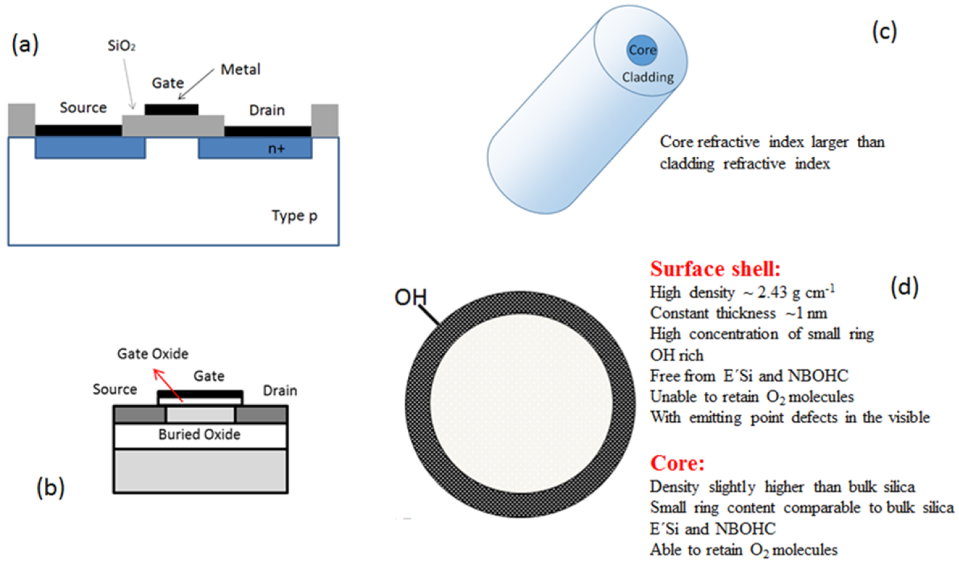
Figure 2.
(a) Model of two SiO2 basic units [6]; (b) Simplified representation of the energy levels of a point defect absorbing (blue arrow) and emitting (red arrow) light at energies lower than the band gap (violet arrow) between valence (VB) and conduction (CB) bands.
Figure 2.
(a) Model of two SiO2 basic units [6]; (b) Simplified representation of the energy levels of a point defect absorbing (blue arrow) and emitting (red arrow) light at energies lower than the band gap (violet arrow) between valence (VB) and conduction (CB) bands.
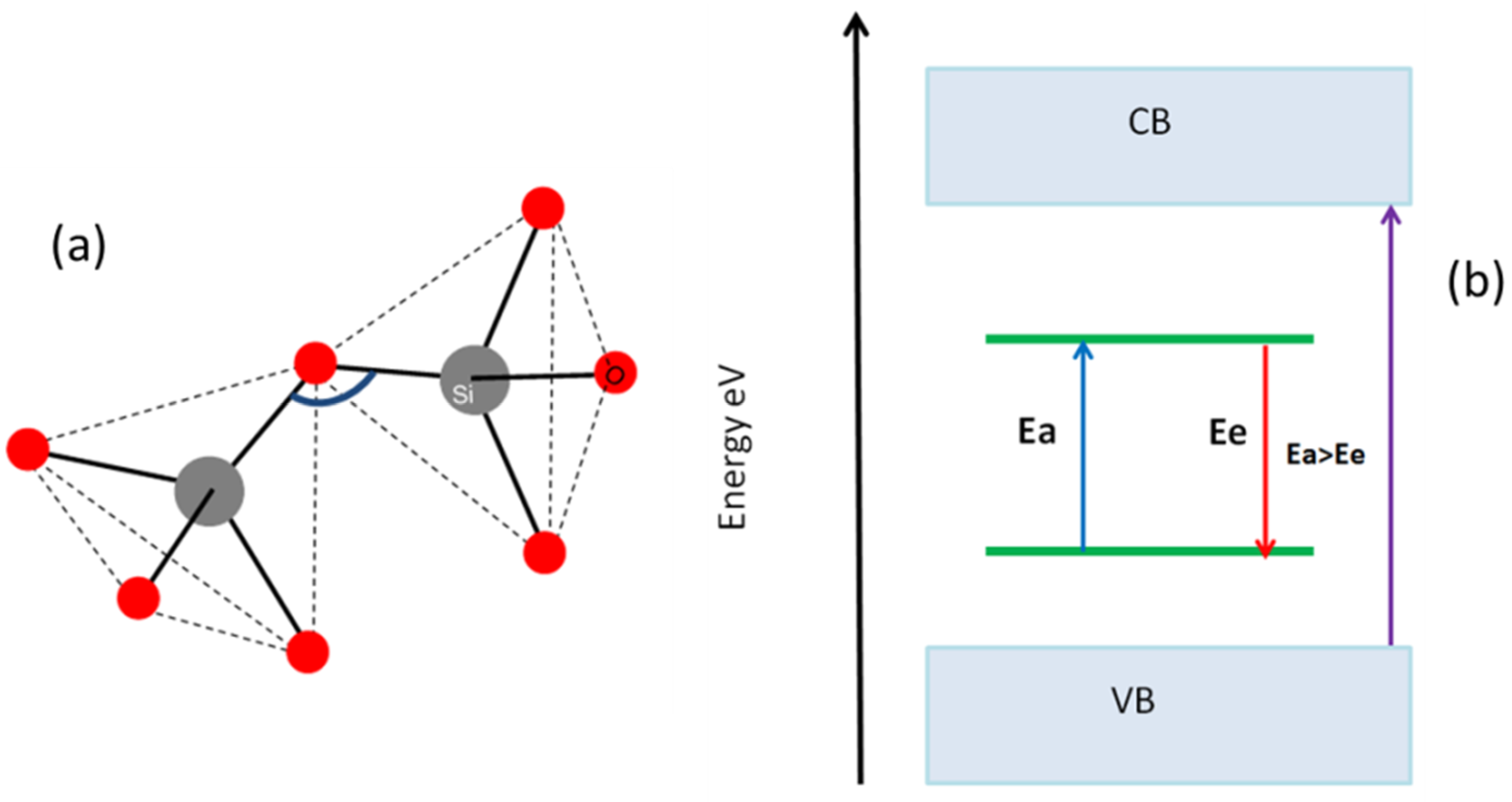
Figure 3.
(a) Structural model of germanium lone pair center (GLPC); (b) Energy levels scheme of GLPC showing the absorptions due to S0–S1 and S0–T1 transitions (black arrows), the emissions due to S1–S0 (violet arrow) and T1–S0 (blue arrow) and the non-radiative transition named intersystem crossing (red dashed arrow); (c) representation of a FBG (fiber Bragg grating), which consists of a periodic alteration of the refractive index.

Figure 4.
(a) Electron trapped in two different sites having different potential wells, which imply different de-trapping behaviors; (b) Dissociation of a molecule following the transition from the ground state to an excited non-bonding state.
Figure 4.
(a) Electron trapped in two different sites having different potential wells, which imply different de-trapping behaviors; (b) Dissociation of a molecule following the transition from the ground state to an excited non-bonding state.
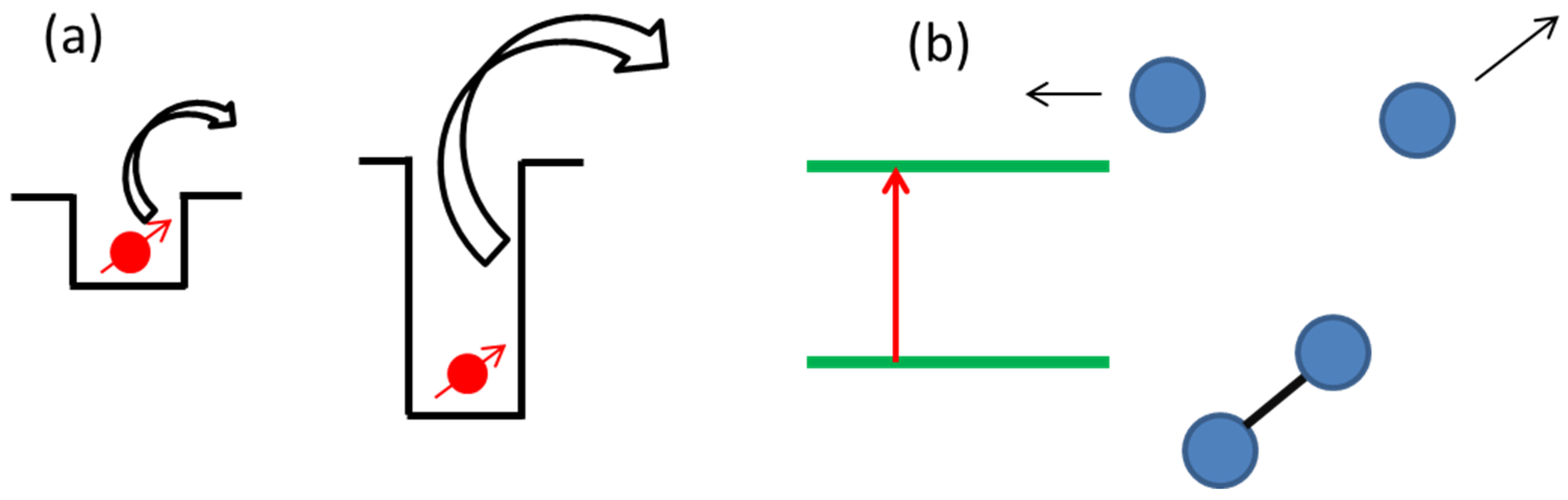
Figure 5.
(a) Optical time domain reflectometry (OTDR) and fiber basic working configuration, the yellow dashed line stands for the pulsed excitation laser injected in the fiber, while the red dashed arrow represents the signal (Rayleigh, Raman, Brillouin) back-scattered by different points of the fiber. Each excitation is followed by back-scattered signals that reach the OTDR with different temporal delays related to the distance from the OTDR allowing the spatially distributed monitoring; (b) Typical OTDR trace recorded in a fiber that features different radiation-induced attenuation (RIA), such as for example as a consequence of a difference in the absorbed dose. The Lambert–Beer law allows evaluating the RIA, and in P-doped fiber, the dose [118].


Table 1.
Defect name, positive and negative effects on silica properties/application and a process that normally implies their generation. MCVD: modified chemical vapor deposition.
Table 1.
Defect name, positive and negative effects on silica properties/application and a process that normally implies their generation. MCVD: modified chemical vapor deposition.
| Defect | Positive | Negative | Generation | Ref |
|---|---|---|---|---|
| SiOH | For nanoparticles functionalization. H2 loading for UV-visible and photosensitivity. | Telecom fiber. They are precursors of NBOHC defects absorbing in the UV-visible. | Usually high content in sol–gel. During nanoparticles production. Low in MCVD, or similar fiber preform manufacturing process. | [27,28,29] [45,50,51,52,53,54,55] |
| Cl related defects | For telecom fiber, Si–Cl helps to reduce the OH content. | For transmission in UV-visible during irradiation. | Some during preform manufacturing. Other absorbing during irradiation. | [7,9,56,57,58,59,60,61] |
| GLPC | FBG and in general photosensitivity. | Transmission in UV-visible during irradiation. | During preform collapse and fiber drawing. | [6,25,65] [72,73,74,75,76,77] [80,81,82,83,84,85,86,87] |
| E’Si | To study density and photo-induced processes. Their absorption is far from transmission windows. | When generated from strained bonds, their generation implies the generation of NBOHC absorbing in UV-visible. | During preform collapse and fiber drawing. During any irradiation. | [6,12,17,18,19,20] [68,70,71] [99,100,101,102,103,104,105] |
| NBOHC | They can be studied with micrometric spatial resolution in fibers to improve fiber characterization. | UV-visible absorption. | During preform collapse and fiber drawing. During any irradiation. | [6,9,17] [45,46,47] [51,52,53,56] [64,65] |
| Strained bonds | Can be used to improve photosensitivity, since they are precursors of absorbing defects, such as, but not only, E’Si and NBOHC. | As defects precursors, their presence implies high RIA, which is a limit for signal transmission from the visible to NIR spectral range and for some distributed sensors. | During preform collapse and fiber drawing. | [7,9,17,18,19,20,21,22,23,24] [69,70] [45,47,48,50] |
| Not fully attributed NIR absorbing defects | Perhaps usable to increase the photosensitivity. | They limit the lengths of employable fiber for transmission and monitoring | During irradiation. | [7,9,69] |
| P1 | Fundamental for fiber-based dosimetry. | Their generation impacts transmission in telecom windows. | Under irradiation. | [108] [113,114,115,116,117,118] |
© 2019 by the authors. Licensee MDPI, Basel, Switzerland. This article is an open access article distributed under the terms and conditions of the Creative Commons Attribution (CC BY) license (http://creativecommons.org/licenses/by/4.0/).
Share and Cite
MDPI and ACS Style
Alessi, A.; Kuhnhenn, J.; Buscarino, G.; Di Francesca, D.; Agnello, S. The Relevance of Point Defects in Studying Silica-Based Materials from Bulk to Nanosystems. Electronics 2019, 8, 1378. https://doi.org/10.3390/electronics8121378
AMA Style
Alessi A, Kuhnhenn J, Buscarino G, Di Francesca D, Agnello S. The Relevance of Point Defects in Studying Silica-Based Materials from Bulk to Nanosystems. Electronics. 2019; 8(12):1378. https://doi.org/10.3390/electronics8121378
Chicago/Turabian StyleAlessi, Antonino, Jochen Kuhnhenn, Gianpiero Buscarino, Diego Di Francesca, and Simonpietro Agnello. 2019. "The Relevance of Point Defects in Studying Silica-Based Materials from Bulk to Nanosystems" Electronics 8, no. 12: 1378. https://doi.org/10.3390/electronics8121378
Note that from the first issue of 2016, this journal uses article numbers instead of page numbers. See further details here.