Electrostatic-Discharge-Immunity Impacts in 300 V nLDMOS by Comprehensive Drift-Region Engineering


Department of Electronic Engineering, National United University, Miaoli City 36003, Taiwan
*
Author to whom correspondence should be addressed.
Electronics 2019, 8(12), 1469; https://doi.org/10.3390/electronics8121469
Submission received: 1 November 2019
/
Revised: 30 November 2019
/
Accepted: 30 November 2019
/
Published: 3 December 2019
(This article belongs to the Special Issue Intelligent Electronic Devices)
Abstract
:Electrostatic discharge (ESD) events are the main factors impacting the reliability of Integrated circuits (ICs); therefore, the ESD immunity level of these ICs is an important index. This paper focuses on comprehensive drift-region engineering for ultra-high-voltage (UHV) circular n-channel lateral diffusion metal-oxide-semiconductor transistor (nLDMOS) devices used to investigate impacts on ESD ability. Under the condition of fixed layout area, there are four kinds of modulation in the drift region. First, by floating a polysilicon stripe above the drift region, the breakdown voltage and secondary breakdown current of this modulation can be increased. Second, adjusting the width of the field-oxide layer in the drift region when the width of the field-oxide layer is 5.8 μm will result in the minimum breakdown voltage (105 V) but the best secondary breakdown current (6.84 A). Third, by adjusting the discrete unit cell and its spacing, the corresponding improved trigger voltage, holding voltage, and secondary breakdown current can be obtained. According to the experimental results, the holding voltage of all devices under test (DUTs) is greater than that of the reference group, so the discrete HV N-Well (HVNW) layer can effectively improve its latch-up immunity. Finally, by embedding different P-Well lengths, the findings suggest that when the embedded P-Well length is 9 μm, it will have the highest ESD ability and latch-up immunity.
1. Introduction
In recent years, the UHV LDMOS has been implemented in power electronics, Microelectromechanical systems (MEMS) domains, power management circuits, and internet of things (IoT) applications [1,2,3,4,5,6,7,8,9,10,11,12,13,14,15,16]. The power management circuit is also an indispensable project of the internet of things. The internet of things is facing the tricky problem of battery endurance, but it can be improved through the power management circuit [14]. However, high-voltage ICs pose serious risks to electrostatic discharge (ESD), and according to the statistics, the ratio of component failure is nearly half due to ESD damage, so ESD protection for the silicon chips is needed to reduce the number of ESD failures. To achieve effective ESD protection, according to the ESD design window shown in Figure 1, there are three important parameters: trigger voltage (Vt1), holding voltage (Vh), and secondary breakdown current (It2). The trigger voltage must be lower than the core circuit breakdown voltage. However, if a high-voltage transient is injected into a circuit, the protection device should be turned on to bypass the heavy current in order to avoid core circuit destruction. Additionally, these protection devices need to be turned on quickly and can sustain a heavy current. The Float Cum Boost Charger (FCBC) architecture [17] itself is susceptible to large current damage, so a contactor is commonly used to discharge its large voltage/current. The ESD protection component in our paper is also the same as the contactor role, so the UHV nLDMOS component response time (Vt1 related) is a key factor. Therefore, we can find out the Vt1 of the component by using the transmission-line pulse (TLP) system to determine whether the protection component can be turned on quickly under a large voltage/current bombardment to prevent the circuit from being damaged by the instantaneous large voltage and current transient. The holding voltage must be higher than positive supply voltage (VDD), otherwise there is a latch-up risk. The secondary breakdown current is as high as possible because it is defined as a device of ESD ability. Additionally, the whole-chip ESD protection design has been proposed to suggest where the chip should be protected to reduce the ESD risk [18]. The protect method is divided into two types—the first is to design ESD protection circuits, which protect chips by using the gate-couple technique [19,20] and the substrate-trigger technique [20,21]; the second is to design ESD protection devices, which use silicon controlled rectifier (SCR) [22,23], Grounded-gate nMOS (GGnMOS) [24], stacked field-oxide device (FOD) [25], and diodes [26] to protect a chip.
The current crowding effect can often reduce the reliability level of UHV LDMOS [27,28,29]. For example, when the n-type heavily doped (N+) junction edge of the drain side is adjacent to the field oxide, as shown in Figure 2a, a large ESD spike will inject into the N+ junction and then crowd at the edge of the field oxide when an ESD event occurs. If the ESD current is too large because the power is equal to the voltage multiplied by the current, the power dissipation will increase when the current is increased. This causes heat generation at the current gathering location and a current crowding effect can occur, which causes device damage.
In this paper, four kinds of novel modulations are proposed for drift-region engineering in order to strengthen the ESD ability of UHV nLDMOSs. (1) By using a floating polysilicon stripe above the field-oxide layer; (2) shortening the width of the field-oxide layer; (3) discrete HV N-Well layer; and (4) the embedded P-Well, the ESD protection ability can be effectively improved.
2. Layout of UHV Circular nLDMOS Devices under Test (DUTs)
2.1. UHV Circular nLDMOS Reference Group
The cross-sectional view and layout top view of an UHV circular nLDMOS are shown in Figure 2a,b, respectively. Due to the process specifications, a field-oxide layer (FOX) is fabricated above the drift region to enhance the breakdown of the electric field. Due to the operational voltage of UHV applications, the n-type lightly doped HVNW layer is used in the drift region. The PBody and the deep P-Well (DPW) form a RESURF structure, which causes the drift region to be completely depleted and increases the breakdown voltage of the device without increasing the length of the drift region [30]. The polysilicon-stripe (poly2) above the drift region is used to reduce the peak value of the electric field. The traditional UHV ESD protection device adopts the elliptical layout type, but the layout area is huge. In this paper, a circular layout type is adopted, which reduces the layout area and makes the voltage distribution more uniform [31,32]. In order to ensure the normal operation of the device characteristics, a semiconductor curve tracer is used to measure the current-voltage (I-V) curve and the breakdown voltage to assure that the DUTs have the correct output characteristics and the correct breakdown voltage value. When the UHV nLDMOS transistor acts as an ESD protection device, its device configuration forms a GGnMOS structure by grounding the gate electrode, which can discharge the ESD current beneath the parasitic Bipolar junction transistor (BJT). In this paper, all the DUTs are fabricated via a TSMC 0.5 μm BCD process. The channel length (L) is 4 μm, the channel width (W) is 394.4 μm, and the drift region length is 29 μm.
2.2. UHV Circular nLDMOS—Polysilicon-Stripe Modulation above the Drift Region
In this structure, the layout of the polysilicon-stripe varies from spiral type to concentric circle type, as shown in Figure 3. The spiral poly2 starts from the drain-side edge, then passes above the field-oxide layer in the drift region, and finally connects to the source electrode. Initially, when an ESD event occurs, the poly2 contact is damaged due to the excessive current density, which reduces the ESD capability. The concentric poly2 type has multiple concentric circles that float above the drift region. The concentric poly2 type reduces the peak value of the electric field below the FOX and increases the breakdown voltage. Additionally, the floating concentric circle poly2 has no contacts, so it avoids the risk of contact damage.
2.3. UHV Circular nLDMOS—Field-Oxide Width Modulation in the Drift Region
A cross-sectional view and layout top view of the field-oxide width modulation in the drift region are shown in Figure 4a,b, respectively. By shortening the width of the field-oxide layer in the drift region, the equivalent series resistance of this device decreases. The purpose of this is to reduce the device impedance, so the breakdown voltage is also reduced. Due to a strong correlation between the breakdown voltage and the trigger voltage, these devices can be applied for the desired operating voltage applications and are fabricated by the same process. The cell names of the modulation parameter are shown in Table 1.
2.4. UHV Circular nLDMOS—Discrete HV N-Well (HVNW) Layer Modulation in the Drift Region
The cross-sectional view and the layout top view of the discrete HVNW layer modulation in the drift region are shown in Figure 5a,b, respectively. In this architecture, the drift region is designed to be discrete and independent by using layout skills. Furthermore, the poly2 layer is changed to a concentric circle form to evaluate the influence of poly2 concentric circles on the discrete HVNW layer. Due to the fact that the parasitic resistance of n-epi is larger than the HVNW layer, the discrete HVNW layer can upgrade the equivalent resistance of the drift region. The DUTs are divided into two modulation types: a unit cell-size modulation (three cell sizes: 1, 2, and 3 μm) and a unit-cell spacing modulation (cell spacings: 1.34, 2.68, and 4.02 μm). Cell names of the discrete HVNW layer modulation are shown in Table 2.
2.5. UHV Circular nLDMOS—Embedded P-Well Length Modulation in the Drift Region
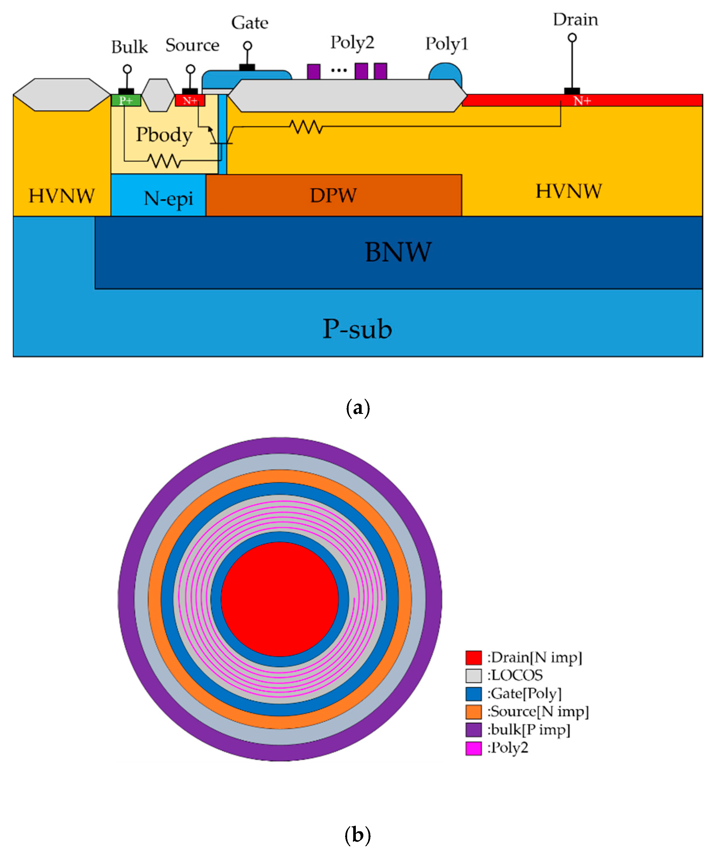
The cross-sectional and layout top views of the embedded P-Well length modulation in the drift region are shown in Figure 6a,b, respectively. Starting from the drain side, the N+ junction edge extends into the local oxidation of silicon (LOCOS) region with an embedded P-Well layer, and the lengths of the extended P-Well (K) are 5, 7, 9, and 11μm. Since the P-Well and N+ regions form a reverse bias junction, when an ESD event occurs, the ESD current flows into the deeper path via the HVNW and BNW layers to avoid device failure due to the current crowding effect at the drain-side LOCOS/N+ edge. The cell names of the embedded P-Well length modulation are shown in Table 3.
3. Testing Machine
The related electronic instruments in a TLP testing system achieve an automated measurement process via the LabVIEW interface. This TLP machine provides a continuous rising square wave to get the I-V curve data of the DUTs. This testing system uses a square wave with 100 ns pulse width and has a short rising/falling time of <10 ns to obtain the voltage and current responses through the DUTs. This short transient pulse is used to simulate the human body model (HBM) waveform of an ESD event. Eventually, the I-V characteristics of the DUTs, such as the trigger voltage, holding voltage, and secondary breakdown current, can be measured.
4. Test Results and Discussion
4.1. UHV Circular nLDMOS—Polysilicon-Stripe Modulation above the Drift Region
The experimental results of the UHV nLDMOS-related DUTs with polysilicon-stripe modulation above the drift region obtained from the breakdown voltage measurement and TLP testing are shown in Table 4. These experiment results demonstrate that the floating poly2 improves the electric field distribution under the field-oxide layer, smoothing the electric field distribution and reducing the peak value of the electric field to enhance the breakdown voltage of a device. The secondary breakdown current is strongly related to the breakdown voltage that a device can withstand. Therefore, in the same device geometries, we find that as the breakdown voltage increases, the secondary breakdown current also increases.
4.2. UHV Circular nLDMOS—Field-Oxide Width Modulation in the Drift Region
The experimental results of the UHV nLDMOS-related DUTs with the field-oxide width modulation in the drift region obtained from the breakdown voltage measurement and TLP testing are shown in Figure 7, Figure 8 and Figure 9. As the field-oxide width decreases, the the equivalent series resistance, the breakdown voltage, and the trigger voltage are significantly reduced, and the holding voltage also lowers. Interestingly, the secondary breakdown currents of the ESD capability were higher than that of the reference group. It appears that the higher the operation voltage is, the lower It2 value it has. The test results of the UHV nLDMOS with field-oxide width modulation in the drift region are shown in Table 5.
4.3. UHV Circular nLDMOS—Discrete HVNW Layer Modulation in the Drift Region
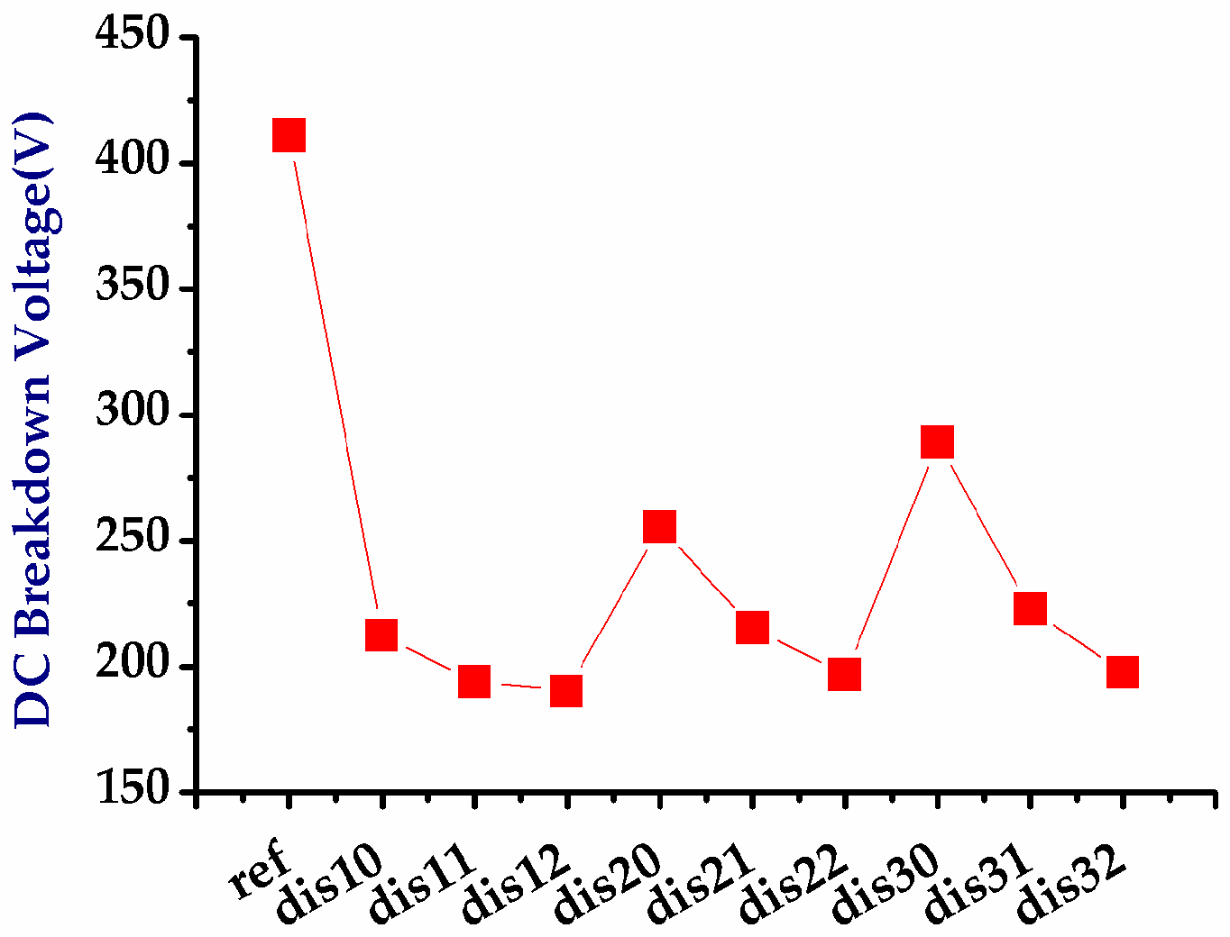
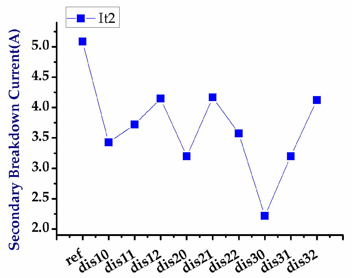
Similarly, the experimental results of the UHV nLDMOS-related DUTs with discrete HVNW layer modulation in the drift region obtained from using the breakdown voltage measurement and TLP testing are shown in Figure 10, Figure 11 and Figure 12. In Figure 10, the breakdown voltage decreases when the HVNW layer is discrete (or experiences an increase in unit cell spacing). Due to the continuous depletion region formed by HVNW/PBody/DPW in the reference device, it can withstand a breakdown voltage of more than 400 V. However, when the HVNW layer was discrete, the breakdown voltage decreased due to the discontinuous depletion layer, which cause the maximum electric breakdown decreased. Figure 11 and Figure 12 demonstrate that since the concentration of the n-epi layer is lower than the HVNW layer, the holding voltages of these HVNW discrete devices are higher than the reference group voltages, because the concentration is inversely proportional to resistivity, which means that the equivalent resistance of the n-epi is indeed higher than that of the HVNW layer. The test results of the UHV nLDMOS with discrete HVNW layer modulation in the drift region are shown in Table 6.
4.4. UHV Circular nLDMOS—Embedded P-Well Length Modulation in the Drift Region
Finally, the experimental results of the UHV nLDMOS-related DUTs with embedded P-Well length modulation in the drift region obtained from the breakdown voltage measurement and TLP testing are shown in Figure 13, Figure 14 and Figure 15. The trigger voltage and the holding voltage increase when the current flow path is blocked by the P-Well, due to the N+/P-Well reverse bias junction, which results in an increase in the turn-on resistance. Nevertheless, even when the trigger voltage slightly decreases, the holding voltage increases related to the increase in P-Well length. When the P-Well length is 9 μm, the trigger voltage is the lowest and the holding voltage (65.5 V) is the highest. Meanwhile, its secondary breakdown current can be reached at 2.47 A, which is the best among the modulation samples. The test results of the modulations of UHV nLDMOS with embedded P-Well in the drift region are shown in Table 7.
5. TCAD Simulation
To verify the differences, the impact generation rate profiles of the UHV nLDMOS transistors with (a) a reference device and (b) an embedded 9 μm P-Well in the drift region structures under the VG = VS= VBulk = 0 V and VD = 310 V conditions are shown in Figure 16a,b. According to these three-dimensional (3-D) TCAD simulations, the general impact ionization process is described by Equation (1) [33]. Here, G represents the generation rate of the electron-hole pairs, and a device will fail if the G value is too high as in the reference DUT in Figure 16a The ionization coefficients for electrons and holes are αn,p, and these coefficients describe the number of electron-hole pairs generated per unit distance traveled by a solitary carrier between two collisions. Their current densities are represented by Jn,p. The impact generation rate profile of the reference device is higher than that of the embedded P-Well modulation. The minority carriers contribute to the drain current, and the majority of carriers are attracted and collected by the bulk electrode, thereby generating the bulk current. As the bulk current continues to increase, the additional carriers increase the forward currents in the transistors. Increasing the currents leads to massive growth heat generation that can lead to a device failure. Therefore, for ESD, latch-up immunities, and breakdown voltage performance, the embedded 9 μm P-Well in the drift region is the most suitable structure for drain-end modulated engineering.
6. Conclusions
Four kinds of modulations are used in circular UHV nLDMOS drift-region engineering: (1) changing the layout of the poly2 layer, (2) field-oxide width modulation, (3) discrete HVNW layer, and (4) embedded P-Well in the drift region. In the first type of modulation, the breakdown voltage increased more than 400 V due to the reduction of the peak electric field and an increase in the secondary breakdown current up to 5 A also occurred. In the second modulation, the breakdown voltage of the drain region reached 105 V, which meant that the operating voltage of the high-voltage circuits could be adjusted by the modulation length of the drift region. For the third modulation, the trigger voltage, holding voltage, and breakdown voltage were adjusted for different application voltages by adjusting the discrete unit cell size and spacing. Finally, for the embedded P-Well of different lengths in the drift region, when the embedded P-Well length was 9 μm, it had the best ESD ability due to the reduction of the impact ionization.
Author Contributions
Conceptualization, P.-L.L.; Formal analysis, P.-L.L.; Investigation, S.-K.F.; Project administration, S.-L.C.; Supervision, S.-L.C.; Validation, P.-L.L.; Writing—original draft, P.-L.L.; Writing—review and editing, S.-L.C.
Funding
This research was no external funding.
Acknowledgments
In this work, authors would like to thank the Taiwan Semiconductor Research Institute in Taiwan for providing the process information and fabrication platform.
Conflicts of Interest
The authors declare no conflict of interest.
References
- Qiao, M.; Zhang, K.; Zhou, X.; Zou, J.; Zhang, B.; Li, Z. 250 V Thin-Layer SOI Technology with Field pLDMOS for High-Voltage Switching IC. IEEE Trans. Electron Devices 2015, 62, 1970–1976. [Google Scholar] [CrossRef]
- Chen, Y.; Chang, C.; Yang, P. A Novel Primary-Side Controlled Universal-Input AC–DC LED Driver Based on a Source-Driving Control Scheme. IEEE Trans. Power Electron. 2015, 30, 4327–4335. [Google Scholar] [CrossRef]
- Chen, Z.; Salman, A.; Mathur, G.; Boselli, G. Design and Optimization on ESD Self-Protection Schemes for 700V LDMOS in High Voltage Power IC. In Proceedings of the in 37th Electrical Overstress/Electrostatic Discharge Symposium, Reno, NV, USA, 27 September–2 October 2015. [Google Scholar]
- Cong, L.; Lee, H. A 110-250V 2MHz Isolated DC-DC Converter with Integrated High-Speed Synchronous Three-Level Gate Drive. In Proceedings of the IEEE Energy Conversion Congress and Exposition, Montreal, QC, Canada, 20–24 September 2015; pp. 1479–1484. [Google Scholar]
- Dai, S.; Knepper, R.; Horenstein, M. A 300 LDMOS analog-multiplexed drive for MEMS devices. IEEE Trans. Circuits Syst. I. Reg. Pap. 2015, 62, 2806–2815. [Google Scholar] [CrossRef]
- Yi, B.; Chen, X. A 300-V Ultra-Low-Specific On-Resistance High-Side p-LDMOS With Auto-Biased n-LDMOS for SPIC. IEEE Trans. Power Electron. 2017, 32, 551–560. [Google Scholar] [CrossRef]
- Chang, C.; Jiang, T.; Yang, P.; Xu, Y.; Xu, C.; Chen, Y. Adaptive line voltage compensation scheme for a source-driving controlled AC–DC LED driver. IET Circuits Devices Syst. 2017, 11, 21–28. [Google Scholar] [CrossRef]
- Kim, S.; LaFonteese, D.; Zhu, D.; Sridhar, D.S.; Pendharkar, S.; Endoh, H.; Boku, K. A new ESD self-protection structure for 700V high side gate drive IC. In Proceedings of the 29th International Symposium on Power Semiconductor Devices and IC’s, Sapporo, Japan, 28 May–1 June 2017; pp. 467–470. [Google Scholar]
- Ker, M.; Lin, C.; Wu, Y.; Wang, W. ESD Protection Design with Low-Leakage Consideration for Silicon Chips of loT Applications. In Proceedings of the 7th Annual IEEE International Conference on Cyber Technology in Automation, Control and Intelligent Systems, Honolulu, HI, USA, 31 July–4 August 2017; pp. 1496–1499. [Google Scholar]
- Wu, J.; Lyu, X.; Kong, M.; Yi, B.; Chen, X. A novel level-shifter integrated on the edge termination region of the high voltage device. In Proceedings of the TENCON 2017 IEEE Region 10 Conference, Penang, Malaysia, 5–8 November 2017; pp. 2683–2686. [Google Scholar]
- Li, W.; Makuuchi, M.; Chujo, N. Design of High-Voltage and High-Speed Driver. In Proceedings of the IEEE 12th International Conference on Power Electronics and Drive Systems, Honolulu, HI, USA, 12–15 December 2017; pp. 448–452. [Google Scholar]
- Sun, W.; Ye, R.; Liu, S.; Wei, J.; Su, W.; Lin, F.; Sun, G.; Lin, Z. Layout Arrangement Concern for Lateral DMOS With Large Geometric Array Used as Output Device. IEEE Trans. Device Mater. Reliab. 2017, 17, 450–457. [Google Scholar] [CrossRef]
- Yi, B.; Cheng, J.; Chen, X. A High-Voltage Quasi-p-LDMOS Using Electrons as Carriers in Drift Region Applied for SPIC. IEEE Trans. Power Electron. 2018, 33, 3363–3374. [Google Scholar] [CrossRef]
- Adila, A.; Husam, A.; Husi, G. Towards the Self-Powered Internet of Things (IoT) by Energy Harvesting: Trends and Technologies for Green IoT. In Proceedings of the 2nd International Symposium on Small-scale Intelligent Manufacturing Systems, Cavan, Ireland, 16–18 April 2018. [Google Scholar]
- Wang, H.; Qiao, M.; Jin, F.; Yu, Y.; Yuan, Z.Y.; Miao, B.; Yang, W.; Wu, J.; Qian, W.; Deng, T.; et al. A 0.35 μm 600 V Ultra-Thin Epitaxial BCD Technology for High Voltage Gate Driver IC. In Proceedings of the 30th International Symposium on Power Semiconductor Devices and ICs, Chicago, IL, USA, 13–17 May 2018; pp. 311–314. [Google Scholar]
- Guo, S.; Chen, X. A Novel p-LDMOS Additionally Conducting Electrons by Control ICs. IEEE J. Electron Devices Soc. 2019, 7, 710–716. [Google Scholar] [CrossRef]
- Mohammadi, F. Operation and Analysis of Float Cum Boost Charger in High-Voltage Switchgear Backup System. In Proceedings of the 1st International Conference on Modern Approaches in Engineering Science (ICMAES), Tbilisi, Georgia, 21 November 2018. [Google Scholar]
- Ker, M. Whole-Chip ESD Protection Design with Efficient VDD-to-VSS ESD Clamp Circuits for Submicron CMOS VLSI. IEEE Trans. Electron Devices 1999, 46, 173–183. [Google Scholar]
- Ker, M.; Chang, H.; Wu, C. A gate-coupled PTLSCR/NTLSCR ESD protection circuit for deep-submicron low-voltage CMOS ICs. IEEE J. Solid-State Circuits 1997, 32, 38–51. [Google Scholar]
- Chen, T.; Ker, M. Investigation of the Gate-Driven Effect and Substrate-Triggered Effect on ESD Robustness of CMOS Devices. IEEE Trans. Device Mater. Reliab. 2001, 1, 190–203. [Google Scholar] [CrossRef]
- Wang, C.; Ker, M. ESD Protection Design with Lateral DMOS Transistor in 40-V BCD Technology. IEEE Trans. Electron Devices 2010, 57, 3395–3404. [Google Scholar] [CrossRef]
- Ker, M.; Hsu, K. Latchup-Free ESD Protection Design with Complementary Substrate-Triggered SCR Devices. IEEE J. Solid-State Circuits 2003, 38, 1380–1392. [Google Scholar]
- Ker, M.; Hsu, K. Overview of On-Chip Electrostatic Discharge Protection Design With SCR-Based Devices in CMOS Integrated Circuits. IEEE Trans. Device Mater. Reliab. 2005, 5, 235–249. [Google Scholar]
- Keppens, B.; Mergens, M.P.J.; Trinh, C.S.; Russ, C.C.; Camp, B.V.; Verhaege, K.G. ESD protection solutions for high voltage technologies. In Proceedings of the Electrical Overstress/Electrostatic Discharge Symposium, Grapevine, TX, USA, 19–23 September 2004; pp. 289–298. [Google Scholar]
- Ker, M.; Lin, K. The Impact of Low-Holding-Voltage Issue in High-Voltage CMOS Technology and the Design of Latchup-Free Power-Rail ESD Clamp Circuit for LCD Driver ICs. IEEE J. Solid-State Circuits 2005, 40, 1751–1759. [Google Scholar]
- Lin, C.; Wu, P.; Ker, M. Area-Efficient and Low-Leakage Diode String for On-Chip ESD Protection. IEEE Trans. Electron Devices 2016, 63, 531–536. [Google Scholar] [CrossRef]
- Jiang, L.; Fan, H.; He, C.; Zhang, B. A reduced surface current LDMOS with stronger ESD robustness. In Proceedings of the 11th IEEE International Conference on Solid-State and Integrated Circuit Technology, Xi’an, China, 29 October–1 November 2012. [Google Scholar]
- Wu, C.; Lee, J.; Lien, C. A Novel Drain Design for ESD Improvement of UHV-LDMOS. IEEE Trans. Electron Devices 2015, 62, 4135–4138. [Google Scholar] [CrossRef]
- Yang, F.; Chen, H.; Tian, X.; Bai, Y.; Zhu, Y. Investigation on Current Crowding Effect in IGBTs. IEEE Trans. Electron Devices 2018, 65, 636–640. [Google Scholar] [CrossRef]
- Parpia, Z.; Salama, C.A.T. Optimization of RESURF LDMOS Transistors: An Analytical Approach. IEEE Trans. Electron Devices 1990, 37, 789–796. [Google Scholar] [CrossRef]
- Yang, K.; Guo, Y.; Pan, D.; Zhang, J.; Li, M.; Tong, Y.; He, L.; Yao, J. A Novel Variation of Lateral Doping Technique in SOI LDMOS With Circular Layout. IEEE Trans. Electron Devices 2018, 65, 1447–1452. [Google Scholar] [CrossRef]
- Pjenčák, J.; Agam, M.; Šeliga, L.; Yao, T.; Suwhanov, A. Novel Approach for NLDMOS Performance Enhancement by Critical Electric Field Engineering. In Proceedings of the 30th International Symposium on Power Semiconductor Devices & ICs, Chicago, IL, USA, 13–17 May 2018; pp. 307–310. [Google Scholar]
- Atlas User’s Manual; Silvaco Group Inc.: Santa Clara, CA, USA, 2018.
Figure 1.
Electrostatic discharge (ESD) protection window of a LDMOS.
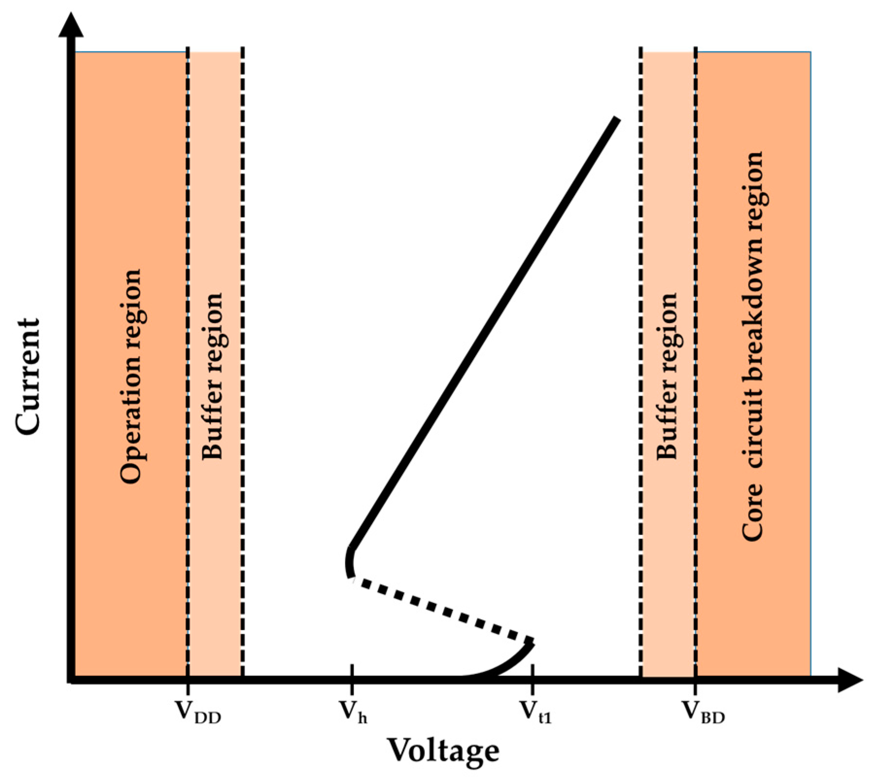
Figure 2.
(a) Cross-sectional view and (b) layout top view of a circular lateral diffusion MOS (nLDMOS).
Figure 2.
(a) Cross-sectional view and (b) layout top view of a circular lateral diffusion MOS (nLDMOS).

Figure 3.
Layout top view of a circular nLDMOS with concentric polysilicon-stripe (poly2) circles.
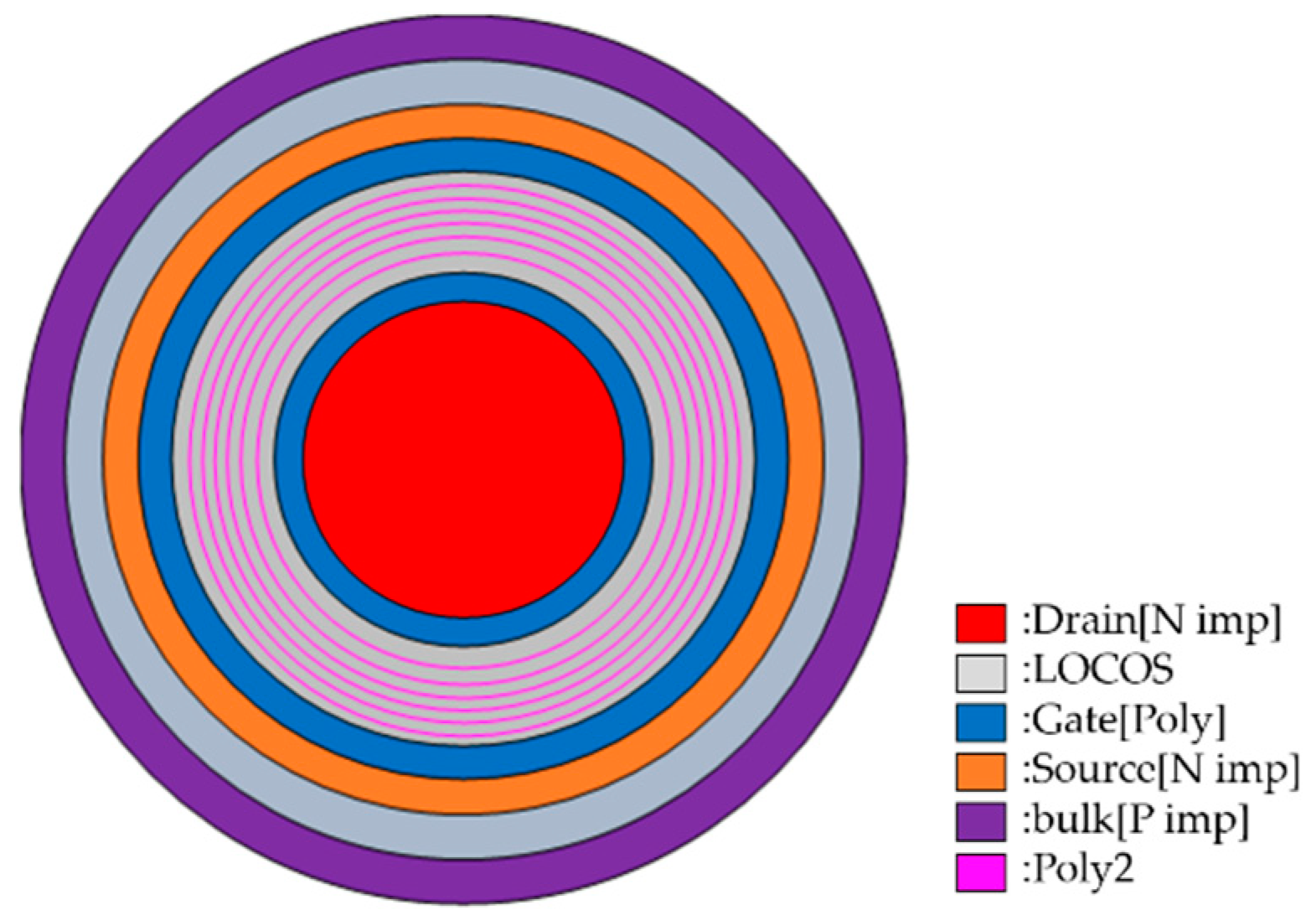
Figure 4.
(a) Cross-sectional view and (b) layout top view of a circular nLDMOS with a field-oxide width modulation in the drift region.
Figure 4.
(a) Cross-sectional view and (b) layout top view of a circular nLDMOS with a field-oxide width modulation in the drift region.
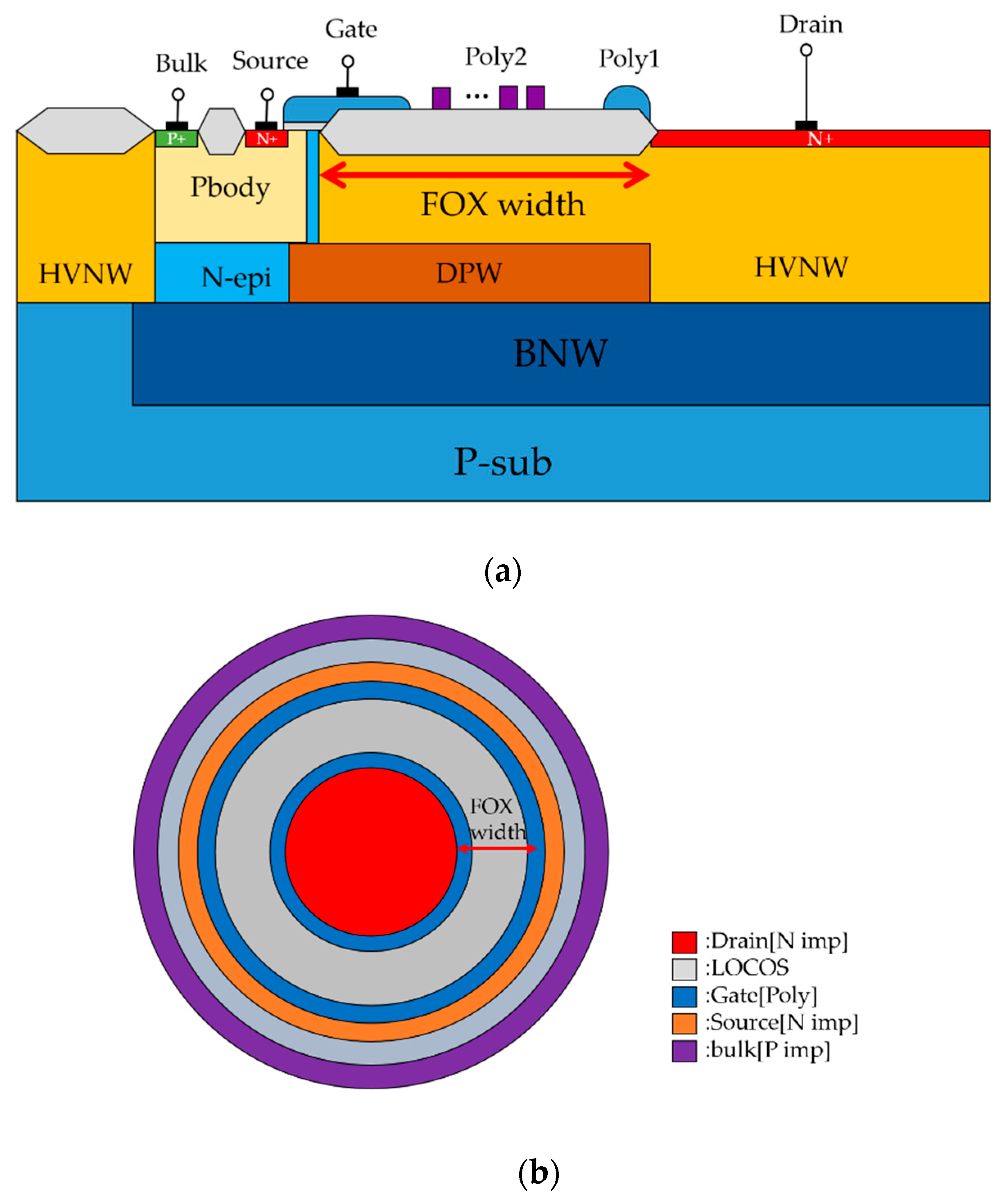
Figure 5.
(a) Cross-sectional view and (b) layout top view of a circular nLDMOS with discrete HV N-Well (HVNW) layer modulation.
Figure 5.
(a) Cross-sectional view and (b) layout top view of a circular nLDMOS with discrete HV N-Well (HVNW) layer modulation.
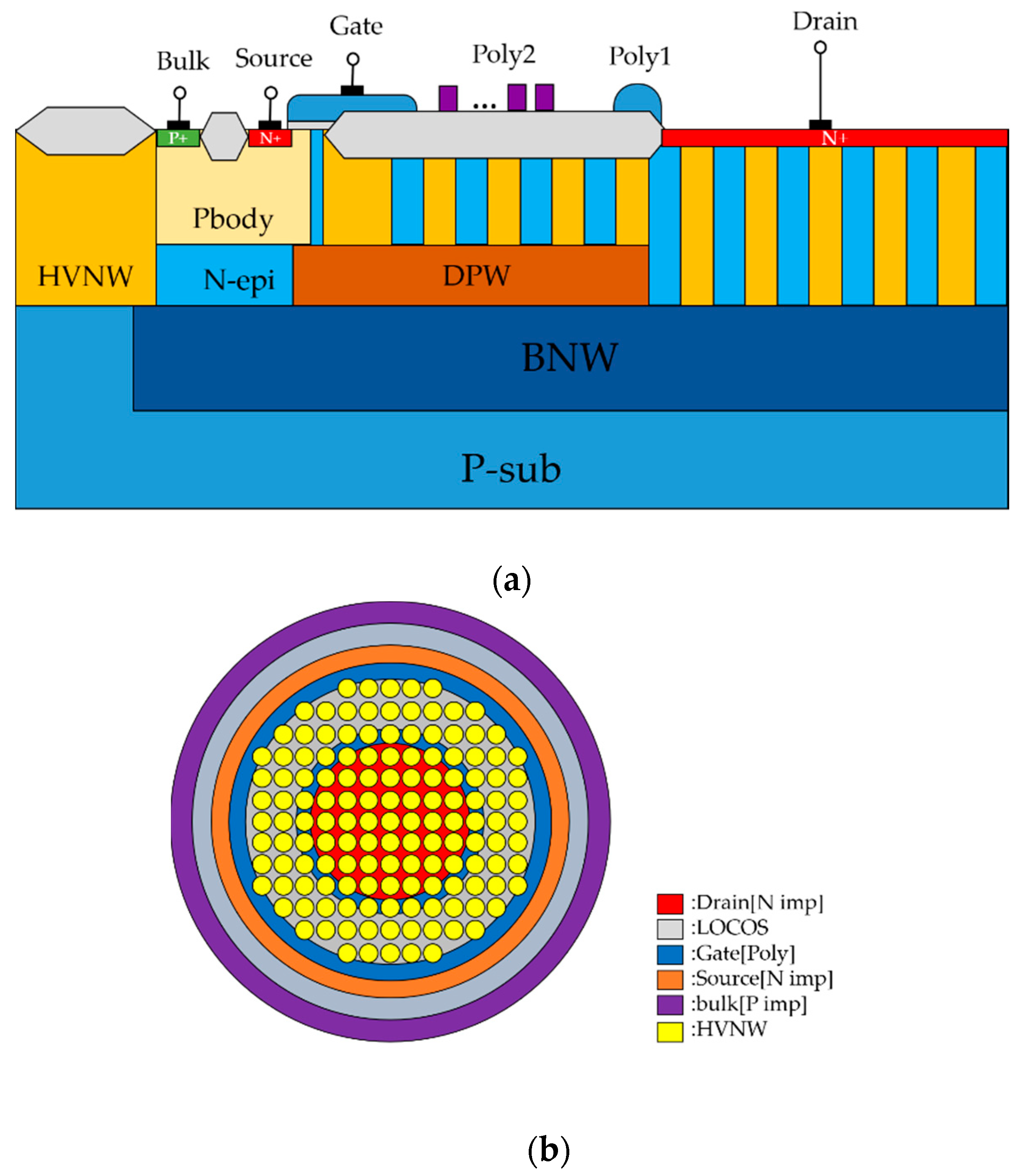
Figure 6.
(a) Cross-sectional view and (b) layout top view of a circular nLDMOS with an embedded P-Well length modulation in the drift region.
Figure 6.
(a) Cross-sectional view and (b) layout top view of a circular nLDMOS with an embedded P-Well length modulation in the drift region.
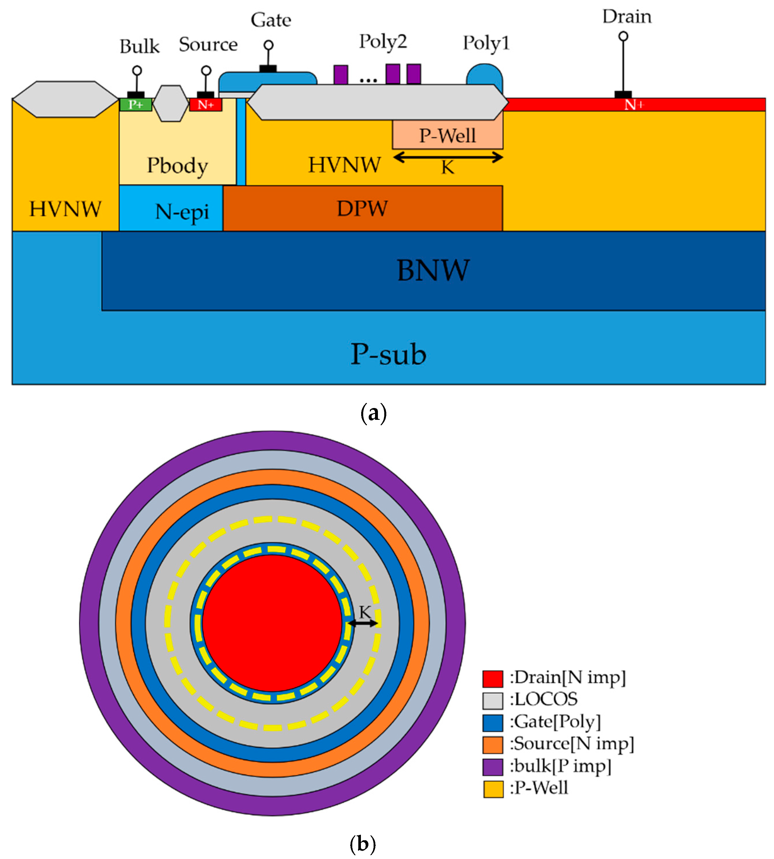
Figure 7.
Breakdown voltage trend chart of nLDMOSs with the field-oxide width modulation in the drift region.
Figure 7.
Breakdown voltage trend chart of nLDMOSs with the field-oxide width modulation in the drift region.

Figure 8.
Secondary breakdown current trend chart of nLDMOSs with the field-oxide width modulation in the drift region.
Figure 8.
Secondary breakdown current trend chart of nLDMOSs with the field-oxide width modulation in the drift region.

Figure 9.
Trigger voltage and holding voltage trend charts of nLDMOSs with the field-oxide width modulation in the drift region.
Figure 9.
Trigger voltage and holding voltage trend charts of nLDMOSs with the field-oxide width modulation in the drift region.
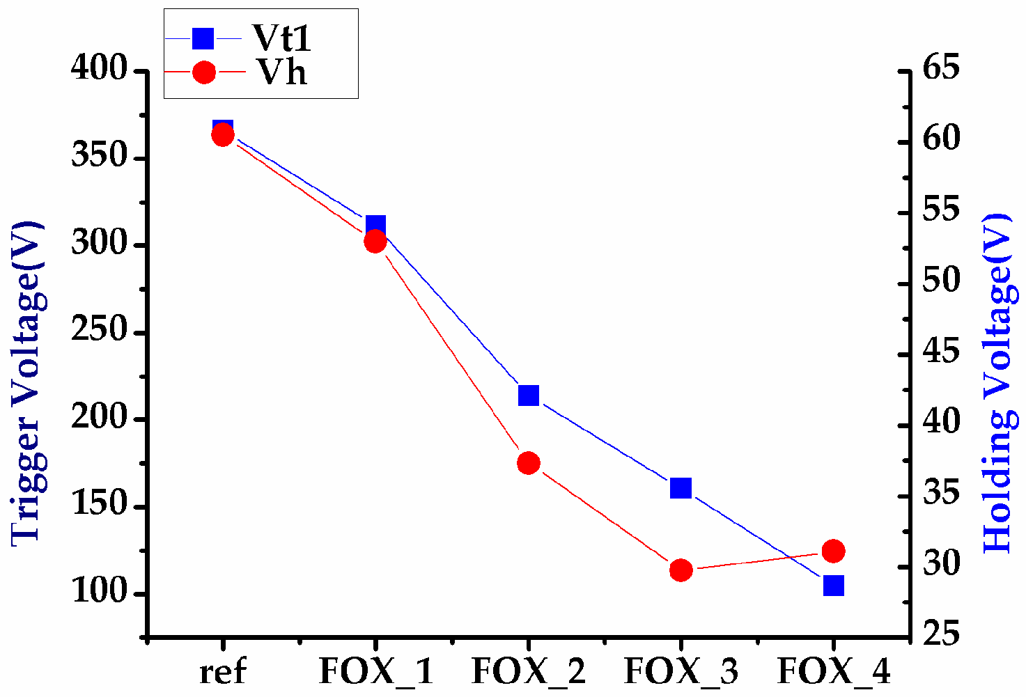
Figure 10.
Breakdown voltage trend chart of nLDMOSs with the discrete HVNW layer modulation in the drift region.
Figure 10.
Breakdown voltage trend chart of nLDMOSs with the discrete HVNW layer modulation in the drift region.

Figure 11.
Secondary breakdown current trend chart of nLDMOSs with the discrete HVNW layer modulation in the drift region.
Figure 11.
Secondary breakdown current trend chart of nLDMOSs with the discrete HVNW layer modulation in the drift region.

Figure 12.
Trigger voltage and holding voltage trend charts of nLDMOSs with the discrete HVNW layer modulation in the drift region.
Figure 12.
Trigger voltage and holding voltage trend charts of nLDMOSs with the discrete HVNW layer modulation in the drift region.
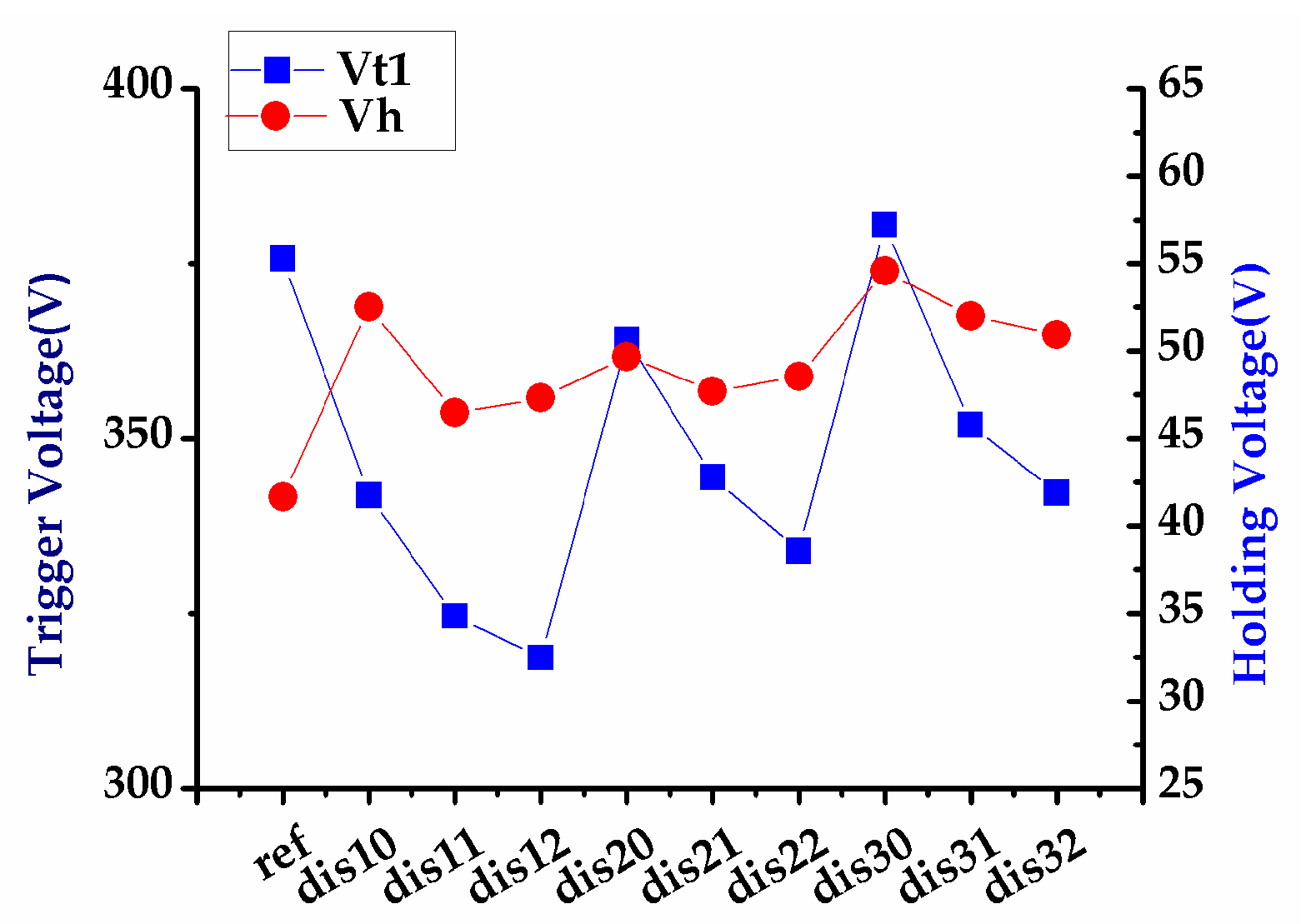
Figure 13.
Breakdown voltage trend chart of nLDMOSs with the embedded P-Well length modulation in the drift region.
Figure 13.
Breakdown voltage trend chart of nLDMOSs with the embedded P-Well length modulation in the drift region.
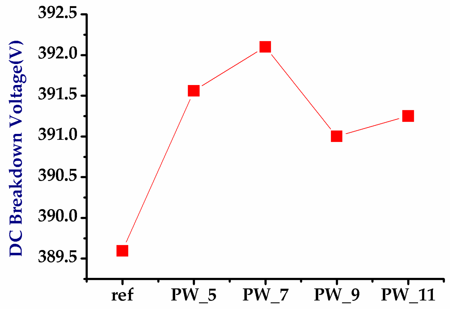
Figure 14.
Secondary breakdown current trend chart of nLDMOSs with the embedded P-Well length modulation in the drift region.
Figure 14.
Secondary breakdown current trend chart of nLDMOSs with the embedded P-Well length modulation in the drift region.
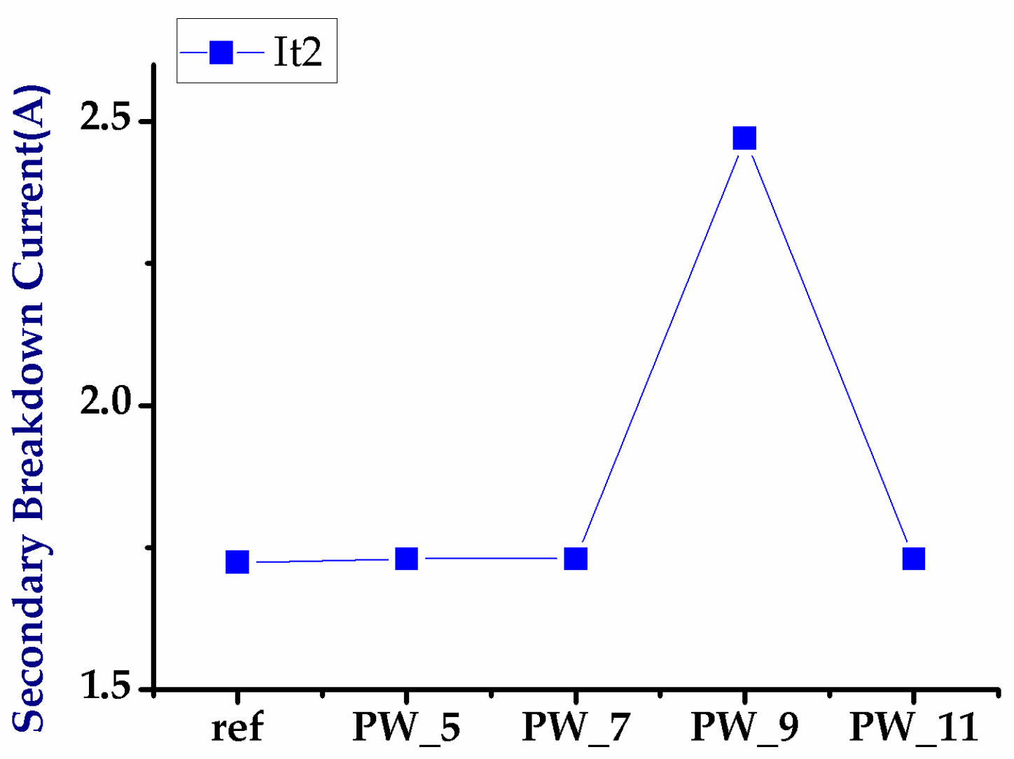
Figure 15.
Trigger voltage and holding voltage trend chart of nLDMOSs with the embedded P-Well length modulation in the drift region.
Figure 15.
Trigger voltage and holding voltage trend chart of nLDMOSs with the embedded P-Well length modulation in the drift region.
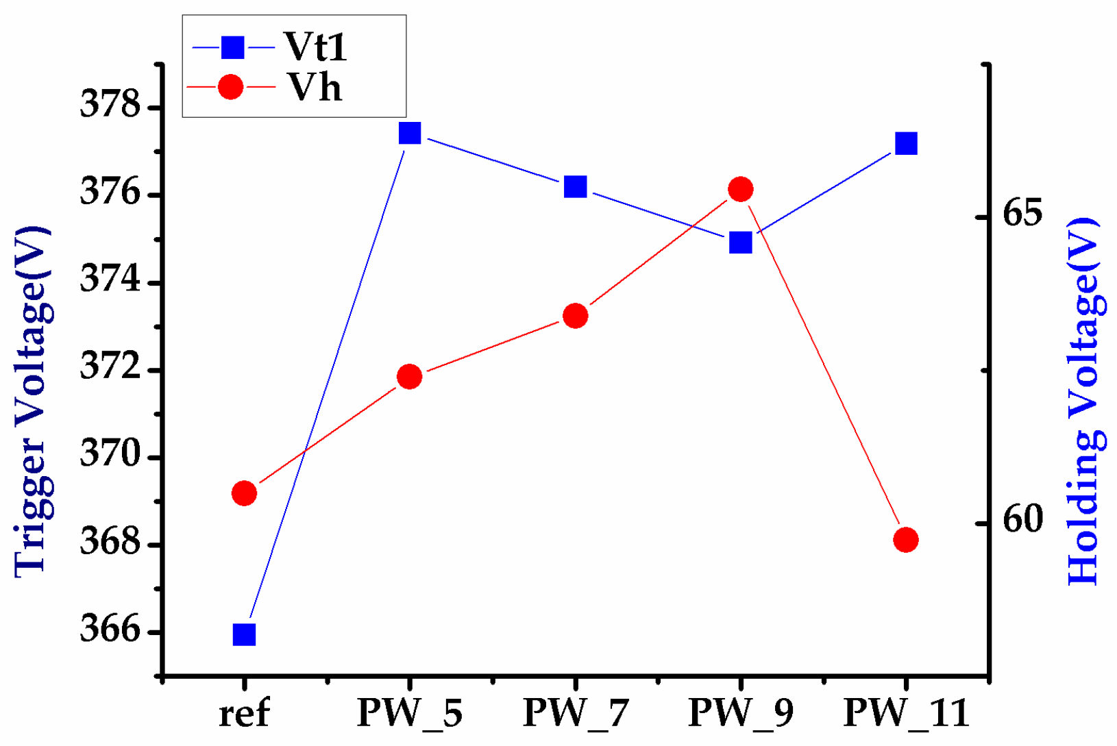
Figure 16.
Impact generation rate diagrams of (a) reference device and (b) embedded 9 μm P-Well in the drift region (full scale: 1 × 10⁻⁷ A/cm2) as the VG = VS= Vbulk = 0 V, VD = 310 V bias condition.
Figure 16.
Impact generation rate diagrams of (a) reference device and (b) embedded 9 μm P-Well in the drift region (full scale: 1 × 10⁻⁷ A/cm2) as the VG = VS= Vbulk = 0 V, VD = 310 V bias condition.


Table 1.
Cell names of the field-oxide width modulation.
| Samples Name | Field-Oxide Width (μm) |
|---|---|
| Ref. | 29 |
| FOX_1 | 23.2 |
| FOX_2 | 17.4 |
| FOX_3 | 11.6 |
| FOX_4 | 5.8 |
Table 2.
Cell names of the discrete HVNW layer modulation.
| Size | 1 μm | 2 μm | 3 μm | |
|---|---|---|---|---|
| Space | ||||
| 1.34 μm | dis10 | dis20 | dis30 | |
| 2.68 μm | dis11 | dis21 | dis31 | |
| 4.02 μm | dis12 | dis22 | dis32 | |
Table 3.
Cell names of the embedded P-Well length modulation.
| Samples Name | P-Well Length (μm) |
|---|---|
| Ref. | 0 |
| PW_5 | 5 |
| PW_7 | 7 |
| PW_9 | 9 |
| PW_11 | 11 |
Table 4.
Snapback parameters of ultra-high-voltage (UHV) nLDMOS-related devices under test (DUTs).
| Samples | Vt1(V) | Vh(V) | It2(A) | VBK(V) |
|---|---|---|---|---|
| Spiral type | 375.13 | 58.69 | 3.20 | 395.12 |
| Concentric circle type | 375.71 | 41.66 | 5.09 | 411.20 |
Table 5.
Snapback parameters of field-oxide width modulation in the drift region.
| Samples | Vt1(V) | Vh(V) | It2(A) | VBK(V) | |
|---|---|---|---|---|---|
| Ref. nLDMOS | 364.44 | 60.49 | 2.46 | 389.59 | |
| FOX width | FOX_1 | 311.40 | 52.97 | 3.65 | 269.85 |
| FOX_2 | 213.88 | 37.34 | 2.99 | 142.25 | |
| FOX_3 | 160.61 | 29.74 | 2.43 | 130.34 | |
| FOX_4 | 104.89 | 31.09 | 6.84 | 105.43 | |
Table 6.
Snapback parameters of discrete HVNW layer modulation in the drift region.
| Samples | Vt1(V) | Vh(V) | It2(A) | VBK(V) | |
|---|---|---|---|---|---|
| Ref. nLDMOS | 375.71 | 41.66 | 5.09 | 411.20 | |
| HVNW discrete | dis 10 | 341.94 | 52.52 | 3.43 | 212.32 |
| dis 11 | 324.67 | 46.48 | 3.72 | 193.79 | |
| dis 12 | 318.69 | 47.31 | 4.15 | 190.29 | |
| dis 20 | 364.15 | 49.65 | 3.20 | 255.48 | |
| dis 21 | 344.48 | 47.72 | 4.17 | 215.27 | |
| dis 22 | 333.98 | 48.52 | 3.57 | 196.76 | |
| dis 30 | 380.50 | 54.60 | 2.22 | 289.29 | |
| dis 31 | 351.92 | 51.99 | 3.20 | 222.75 | |
| dis 32 | 342.27 | 50.95 | 4.12 | 197.62 | |
Table 7.
Snapback parameters of embedded P-Well length modulation in the drift region.
| Samples | Vt1(V) | Vh(V) | It2(A) | VBK(V) | |
|---|---|---|---|---|---|
| Ref. nLDMOS | 364.44 | 60.49 | 1.72 | 389.59 | |
| P-Well | PW_5 | 377.42 | 62.39 | 1.73 | 391.56 |
| PW_7 | 376.195 | 63.39 | 1.73 | 392.10 | |
| PW_9 | 374.92 | 65.46 | 2.47 | 391.00 | |
| PW_11 | 377.19 | 59.72 | 1.73 | 391.25 | |
© 2019 by the authors. Licensee MDPI, Basel, Switzerland. This article is an open access article distributed under the terms and conditions of the Creative Commons Attribution (CC BY) license (http://creativecommons.org/licenses/by/4.0/).
Share and Cite
MDPI and ACS Style
Lin, P.-L.; Chen, S.-L.; Fan, S.-K. Electrostatic-Discharge-Immunity Impacts in 300 V nLDMOS by Comprehensive Drift-Region Engineering. Electronics 2019, 8, 1469. https://doi.org/10.3390/electronics8121469
AMA Style
Lin P-L, Chen S-L, Fan S-K. Electrostatic-Discharge-Immunity Impacts in 300 V nLDMOS by Comprehensive Drift-Region Engineering. Electronics. 2019; 8(12):1469. https://doi.org/10.3390/electronics8121469
Chicago/Turabian StyleLin, Po-Lin, Shen-Li Chen, and Sheng-Kai Fan. 2019. "Electrostatic-Discharge-Immunity Impacts in 300 V nLDMOS by Comprehensive Drift-Region Engineering" Electronics 8, no. 12: 1469. https://doi.org/10.3390/electronics8121469
Note that from the first issue of 2016, this journal uses article numbers instead of page numbers. See further details here.