Electron Affinity and Bandgap Optimization of Zinc Oxide for Improved Performance of ZnO/Si Heterojunction Solar Cell Using PC1D Simulations

Abstract
:
1. Introduction
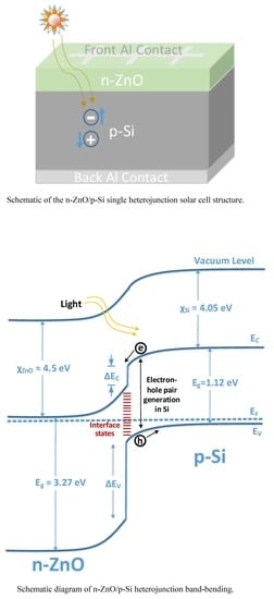
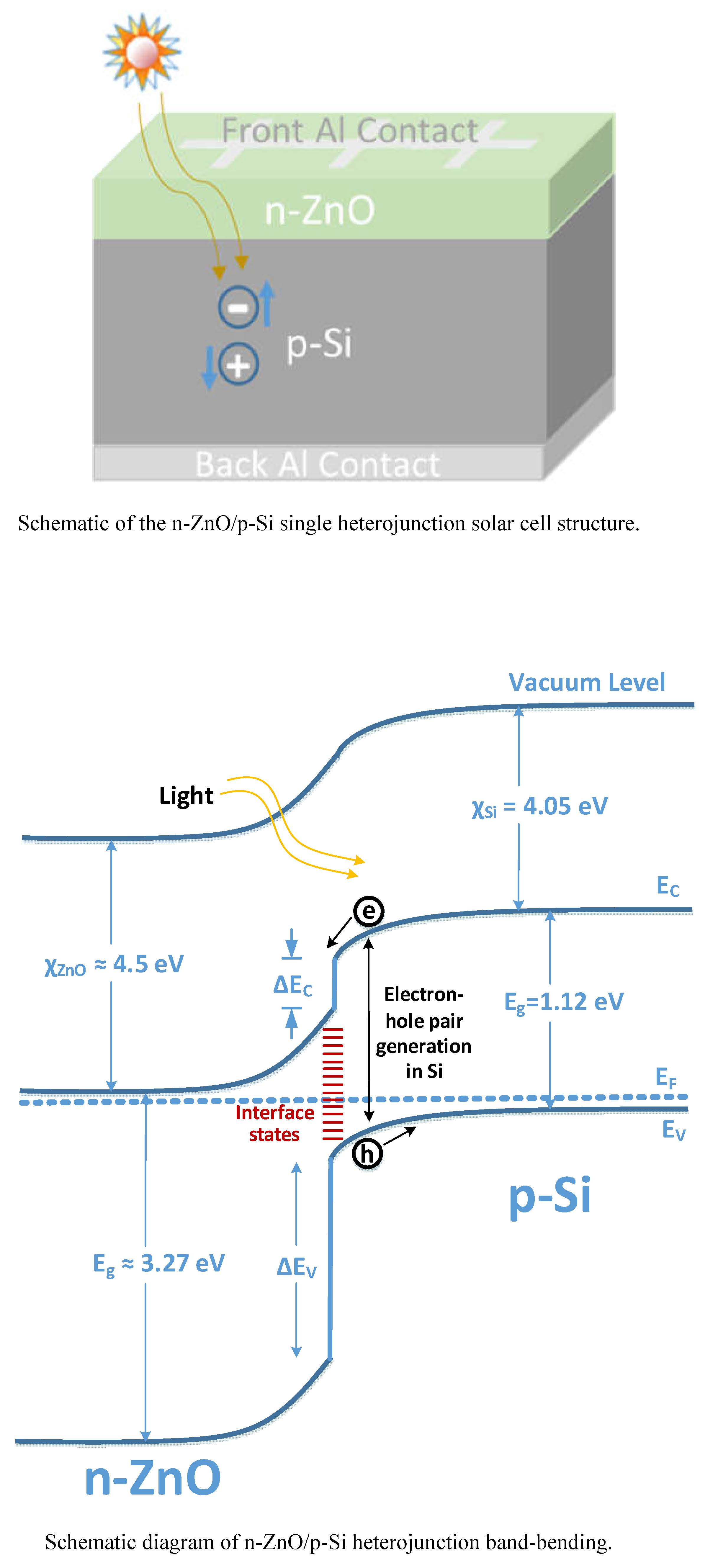
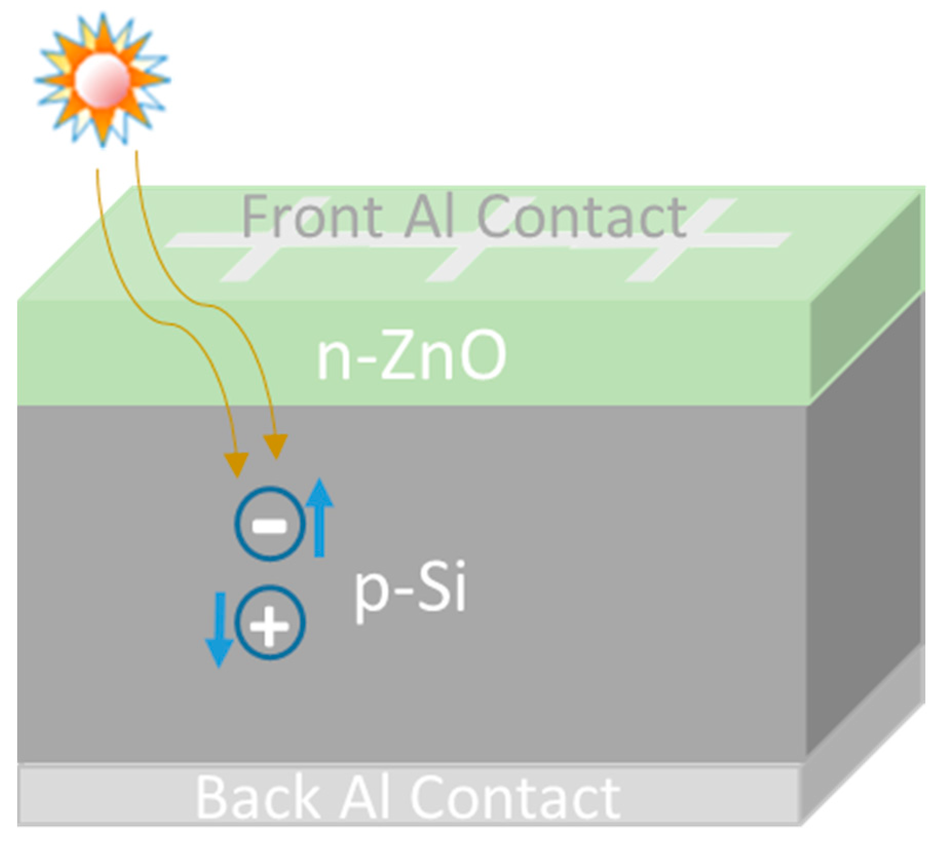
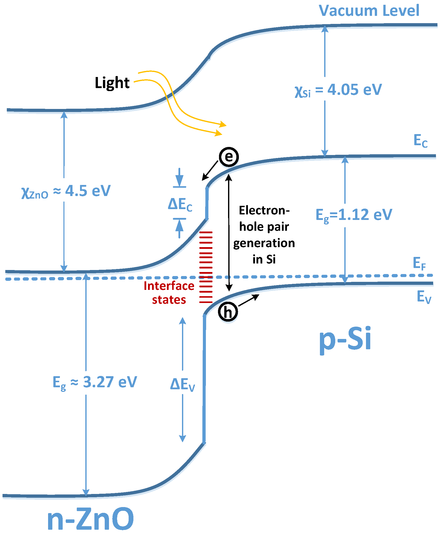
2. Background
3. Results and Analysis
3.1. Personal Computer One Dimensional (PC1D) Simulations
4. Conclusions
Author Contributions
Funding
Acknowledgments
Conflicts of Interest
References
- Hussain, B.; Ebong, A.; Ferguson, I. Zinc oxide as an active n-layer and antireflection coating for silicon based heterojunction solar cell. Sol. Energy Mater. Sol. Cells 2015, 139, 95–100. [Google Scholar] [CrossRef]
- Baturay, S.; Ocak, Y.S.; Kaya, D. The effect of Gd doping on the electrical and photoelectrical properties of Gd:ZnO/p-Si heterojunctions. J. Alloys Compd. 2015, 645, 29–33. [Google Scholar] [CrossRef]
- Ren, X.; Zi, W.; Ma, Q.; Xiao, F.; Gao, F.; Hu, S.; Zhou, Y.; Liu, S.F. Topology and texture controlled ZnO thin film electrodeposition for superior solar cell efficiency. Sol. Energy Mater. Sol. Cells 2015, 134, 54–59. [Google Scholar] [CrossRef]
- Zeng, X.; Wen, X.; Sun, X.; Liao, W.; Wen, Y. Boron-doped zinc oxide thin films grown by metal organic chemical vapor deposition for bifacial a-Si:H/c-Si heterojunction solar cells. Thin Solid Films 2016, 605, 257–262. [Google Scholar] [CrossRef]
- Das, S.C.; Green, R.J.; Podder, J.; Regier, T.Z.; Chang, G.S.; Moewes, A. Band Gap Tuning in ZnO Through Ni Doping via Spray Pyrolysis. J. Phys. Chem. C 2013, 117, 12745–12753. [Google Scholar] [CrossRef]
- Mayer, M.A.; Speaks, D.T.; Yu, K.M.; Mao, S.S.; Haller, E.E.; Walukiewicz, W. Band structure engineering of ZnO1-xSex alloys. In Proceedings of SPIE Volume 7770, Solar Hydrogen and Nanotechnology V, San Diego, CA, USA, 24 August 2010; SPIE: Bellingham, WA, USA. [CrossRef]
- Mayer, M.A.; Yu, K.M.; Haller, E.E.; Walukiewicz, W. Tuning structural, electrical, and optical properties of oxide alloys: ZnO1−xSex. J. Appl. Phys. 2012, 111, 113505. [Google Scholar] [CrossRef]
- Untila, G.; Kost, T.; Chebotareva, A. Bifacial 8.3%/5.4% front/rear efficiency ZnO:Al/n-Si heterojunction solar cell produced by spray pyrolysis. Sol. Energy 2016, 127, 184–197. [Google Scholar] [CrossRef]
- Ahmmed, S.; Aktar, A.; Kuddus, A.; Ismail, A.B.M. Fabrication of Thin-Film Solar Cell using Spin Coated Zinc Oxide and Silicon Nanoparticles Doped Cupric Oxide Heterojunction. In Proceedings of the 2018 International Conference on Computer, Communication, Chemical, Material and Electronic Engineering (IC4ME2), Rajshahi, Bangladesh, 8–9 February 2018; pp. 1–4. [Google Scholar]
- Chen, L.; Chen, X.; Liu, Y.; Zhao, Y.; Zhang, X. Research on ZnO/Si heterojunction solar cells. J. Semicond. 2017, 38, 054005. [Google Scholar] [CrossRef]
- Shokeen, P.; Jain, A.; Kapoor, A. Embedded vertical dual of silver nanoparticles for improved ZnO/Si heterojunction solar cells. J. Nanophoton 2017, 11, 1. [Google Scholar] [CrossRef]
- Hussain, B. Improvement in open circuit voltage of n-ZnO/p-Si solar cell by using amorphous-ZnO at the interface. Prog. Photovolt: Res. Appl. 2017, 25, 919–927. [Google Scholar] [CrossRef]
- Pietruszka, R.; Witkowski, B.; Zielony, E.; Placzek-Popko, E.; Godlewski, M.; Gwozdz, K. ZnO/Si heterojunction solar cell fabricated by atomic layer deposition and hydrothermal methods. Sol. Energy 2017, 155, 1282–1288. [Google Scholar] [CrossRef]
- Ziani, N.; Belkaid, M.S. Computer modeling zinc oxide/silicon heterojunction solar cells. J. Nano Electron. Phys. 2018, 10, 06002. [Google Scholar] [CrossRef]
- Vallisree, S.; Thangavel, R.; Lenka, T.R. Modelling, simulation, optimization of Si/ZnO and Si/ZnMgO heterojunction solar cells. Adv. Mater. Express 2019, 6, 1–20. [Google Scholar] [CrossRef]
- Askari, S.S.A.; Kumar, M.; Das, M.K. Numerical study on the interface properties of a ZnO/c-Si heterojunction solar cell. Semicond. Sci. Technol. 2018, 33, 1–8. [Google Scholar] [CrossRef]
- Sundaram, K.B. Work function determination of zinc oxide films. J. Vac. Sci. Technol. A: Vac. Surf. Films 1997, 15, 428–430. [Google Scholar] [CrossRef]
- Jiang, X.; Jia, C.L.; Szyszka, B. Manufacture of specific structure of aluminum-doped zinc oxide films by patterning the substrate surface. Appl. Phys. Lett. 2002, 80, 3090–3092. [Google Scholar] [CrossRef]
- Lee, J.; Choi, Y.; Kim, J.; Park, M.; Im, S. Optimizing n-ZnO/p-Si heterojunctions for photodiode applications. Thin Solid Films 2002, 403, 553–557. [Google Scholar] [CrossRef]
- Lee, J.; Choi, Y.; Choi, W.; Yeom, H.; Yoon, Y.; Kim, J.; Im, S. Characterization of films and interfaces in n-ZnO/p-Si photodiodes. Thin Solid Films 2002, 420, 112–116. [Google Scholar] [CrossRef]
- Shih, J.-L. Zinc oxide-silicon heterojunction solar cells by sputtering. Master’s Thesis, McGill University, Montreal, QC, Canada, November 2007; p. 118. [Google Scholar]
- Ruan, Y.-C.; Ruan, Y.; Ching, W.Y. An effective dipole theory for band lineups in semiconductor heterojunctions. J. Appl. Phys. 1987, 62, 2885–2897. [Google Scholar] [CrossRef]
- Gopal, V.; Singh, S.; Mehra, R. Analysis of dark current contributions in mercury cadmium telluride junction diodes. Infrared Phys. Technol. 2002, 43, 317–326. [Google Scholar] [CrossRef]
- Kraut, E.A. The effect of a valence-band offset on potential and current distributions in HgCdTe heterostructures. J. Vac. Sci. Technol. A: Vac. Surf. Films 1989, 7, 420–423. [Google Scholar] [CrossRef]
- Hussain, B.; Ali, A.; Unsur, V.; Ebong, A. On structural and electrical characterization of n-ZnO/p-Si single heterojunction solar cell. In Proceedings of the 2016 IEEE 43rd Photovoltaic Specialists Conference (PVSC), Portland, OR, USA, 5–10 June 2016; pp. 1898–1901. [Google Scholar]
- Hussain, B. Development of n-ZnO/p-Si single heterojunction solar cell with and without interfacial layer. Ph.D. Thesis, The University of North Carolina at Charlotte, Charlotte, NC, USA, 2017; p. 154. [Google Scholar]
- Basore, P. Numerical modeling of textured silicon solar cells using PC-1D. IEEE Trans. Electron Devices 1990, 37, 337–343. [Google Scholar] [CrossRef]
- Clugston, D.; Basore, P. PC1D version 5: 32-bit solar cell modeling on personal computers. In Proceedings of the Conference Record of the Twenty Sixth IEEE Photovoltaic Specialists Conference – 1997, Anaheim, CA, USA, 29 September–3 October 1997. [Google Scholar] [CrossRef]
- Zhao, J.; Sun, X.W.; Tan, S.T. Bandgap-Engineered Ga-Rich GaZnO Thin Films for UV Transparent Electronics. IEEE Trans. Electron Devices 2009, 56, 2995–2999. [Google Scholar] [CrossRef]


© 2019 by the authors. Licensee MDPI, Basel, Switzerland. This article is an open access article distributed under the terms and conditions of the Creative Commons Attribution (CC BY) license (http://creativecommons.org/licenses/by/4.0/).
Share and Cite
Hussain, B.; Aslam, A.; Khan, T.M.; Creighton, M.; Zohuri, B. Electron Affinity and Bandgap Optimization of Zinc Oxide for Improved Performance of ZnO/Si Heterojunction Solar Cell Using PC1D Simulations. Electronics 2019, 8, 238. https://doi.org/10.3390/electronics8020238
Hussain B, Aslam A, Khan TM, Creighton M, Zohuri B. Electron Affinity and Bandgap Optimization of Zinc Oxide for Improved Performance of ZnO/Si Heterojunction Solar Cell Using PC1D Simulations. Electronics. 2019; 8(2):238. https://doi.org/10.3390/electronics8020238
Chicago/Turabian StyleHussain, Babar, Aasma Aslam, Taj M Khan, Michael Creighton, and Bahman Zohuri. 2019. "Electron Affinity and Bandgap Optimization of Zinc Oxide for Improved Performance of ZnO/Si Heterojunction Solar Cell Using PC1D Simulations" Electronics 8, no. 2: 238. https://doi.org/10.3390/electronics8020238