Nano-Particle VO2 Insulator-Metal Transition Field-Effect Switch with 42 mV/decade Sub-Threshold Slope


Electrical and Computer Engineering Department, University of Utah, Salt Lake City, UT 84112, USA
*
Author to whom correspondence should be addressed.
Electronics 2019, 8(2), 151; https://doi.org/10.3390/electronics8020151
Submission received: 25 October 2018
/
Revised: 14 January 2019
/
Accepted: 17 January 2019
/
Published: 1 February 2019
(This article belongs to the Special Issue Nanoelectronic Materials, Devices and Modeling)
Abstract
:The possibility of controlling the insulator-to-metal transition (IMT) in nano-particle VO2 (NP-VO2) using the electric field effect in a metal-oxide-VO2 field-effect transistor (MOVFET) at room temperature was investigated for the first time. The IMT induced by current in NP-VO2 is a function of nano-particle size and was studied first using the conducting atomic force microscope (cAFM) current-voltage (I-V) measurements. NP-VO2 switching threshold voltage (VT), leakage current (Ileakage), and the sub-threshold slope of their conductivity (Sc) were all determined. The cAFM data had a large scatter. However, VT increased as a function of particle height (h) approximately as VT(V) = 0.034 h, while Ileakage decreased as a function of h approximately as Ileakage (A) = 3.4 × 10⁻⁸e−h/9.1. Thus, an asymptotic leakage current of 34 nA at zero particle size and a tunneling (carrier) decay constant of ~9.1 nm were determined. Sc increased as a function of h approximately as Sc (mV/decade) = 2.1 × 10⁻³eh/6 and was around 0.6 mV/decade at h~34 nm. MOVFETs composed of Pt drain, source and gate electrodes, HfO2 gate oxide, and NP-VO2 channels were then fabricated and showed gate voltage dependent drain-source switching voltage and current (IDS). The subthreshold slope (St) of drain-source current (IDS) varied from 42 mV/decade at VG = −5 V to 54 mV/decade at VG = +5 V.
1. Introduction
Vanadium dioxide (VO2) is a model insulator–metal transition (IMT) material that displays a first-order transition from a monoclinic insulating phase to a tetragonal metallic phase at a critical temperature (TC) of 341 K in its bulk form [1]. This transition in addition to the semiconductor field-effect in VO2 provides an opportunity to potentially realize switches with steep subthreshold slope of better than 60 mV/decade of silicon for energy efficient devices and applications.
In addition to heat (temperature), the IMT in VO2 can be induced by charge injection, light, mechanical stress, terahertz signals, and many other stimuli. In early reports, the charge-induced IMT was ascribed to local heating of the VO2 material over the critical temperature (TIMT) by the current flowing through the device [2]. Recently, however, other non-thermal mechanisms of the voltage-triggered IMT were proposed [3,4,5]. Specifically, the electric field, rather than local dissipated power due to Joule heating, was suggested to be the origin of the IMT in some cases [2,4,5,6]. Charge injection induced IMT in VO2 was reported in the past and was used to realize negative differential gate capacitance to improve the subthreshold current slope (St) [4]. Additionally, the investigation of electric field effect on the IMT has gained importance as a field-controlled IMT effect in fast and reliable electronic devices.
Our main motivation in this study is to develop field-effect transistor (FET) devices with very steep sub-threshold current slopes for energy efficient switches. In crystalline VO2 the insulating phase carrier concentration is quite high on the order of 1021 cm−3. Therefore, the effect of gate electric field in modulating the IDS is small since the channel has large conductivity to begin with. In VO2 nano-particles and polycrystalline films, small crystalline regions are separated by grain boundary regions that have lower conductivity (n~ 1017–1018 cm−3) [7]. In these materials, the electric field-effect in the boundary regions appears to control the channel turn-on voltage and the sub-threshold current slope as discussed here. The electric field effect and the transition temperature can be related to each other. We have recently shown that the transition temperature in VO2 reduces at higher applied gate voltages, and the relationship is approximately given by: Ttransition = 1.2 VG + 63.8 °C where VG < 0 [7].
Recently, there has been an increased interest in developing high energy efficiency electronic switches using transition metal dichalcogenides [8] and IMT materials [9,10]. The grain size in polycrystalline VO2 affects the IMT temperature as discussed in [11]. We note that to realize efficient transistors, IMT materials are great candidates, since in addition to providing the usual semiconducting carrier control mechanism, they also provide very steep IMT transitions. VO2 has a transition temperature of 63 °C and is used here to demonstrate the feasibility of metal-oxide-VO2 field-effect transistor (MOVFET). A better channel material is Cr-doped V2O3 with possible transition temperature of above 150 °C [12].
2. Nano-Particle Studies
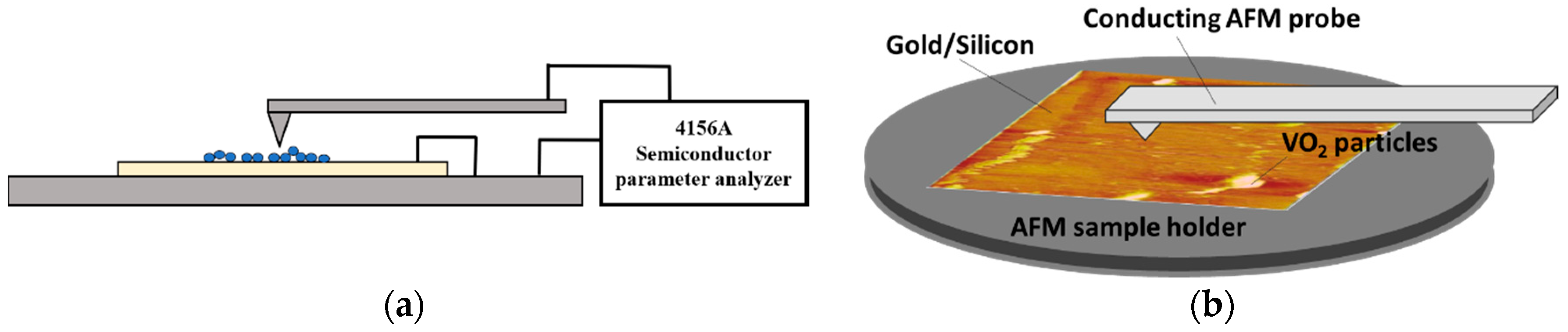
VO2 nano-particles, obtained from Strem Chemicals (Newburyport, MA, USA) [13], were deposited on a gold covered oxidized silicon chip for atomic force microscope (cAFM) studies. To fabricate the chips, we started with a p-type silicon wafer that was cleaned using piranha and buffered oxide etches. Subsequently, the silicon was oxidized (~90 nm) using wet thermal oxidation and then it was coated with 100 nm of Au on 20 nm of Ti adhesion layer. Finally, the wafer was diced into 1 cm2 square chips suitable for cAFM scans and measurements (Figure 1). The VO2 powder was mixed with ethanol and ultra-sonicated for 3 min to prevent agglomeration. The mixture was poured over the central region of the gold-covered silicon chip (Figure 1b) and allowed to dry to obtain evenly spread VO2 particles over the sample. Conductive atomic force microscopy (cAFM) measurements were then carried out on a Multimode AFM using a Pt conducting tip connected to a semiconductor parameter analyzer for I-V measurements (Figure 1a). To measure the thickness of each particle, we used the metrology capability of the AFM system that provided a numerical value for particle height. We assumed that the particles are spherical and used the particle height as its diameter. The I-V measurements were carried out by locating a VO2 particle using the cAFM probe, which also acted as the top contact to the particle with the gold substrate as the bottom contact. All experiments were done at room temperature.
Figure 1c shows a representative AFM scan performed over the Au substrate containing VO2 particles. A wide distribution of particle heights was obtained during a single scan. Particle heights were determined using AFM line scans shown by dashed lines in Figure 1c and displayed with numerical values by the AFM software in Figure 1d.
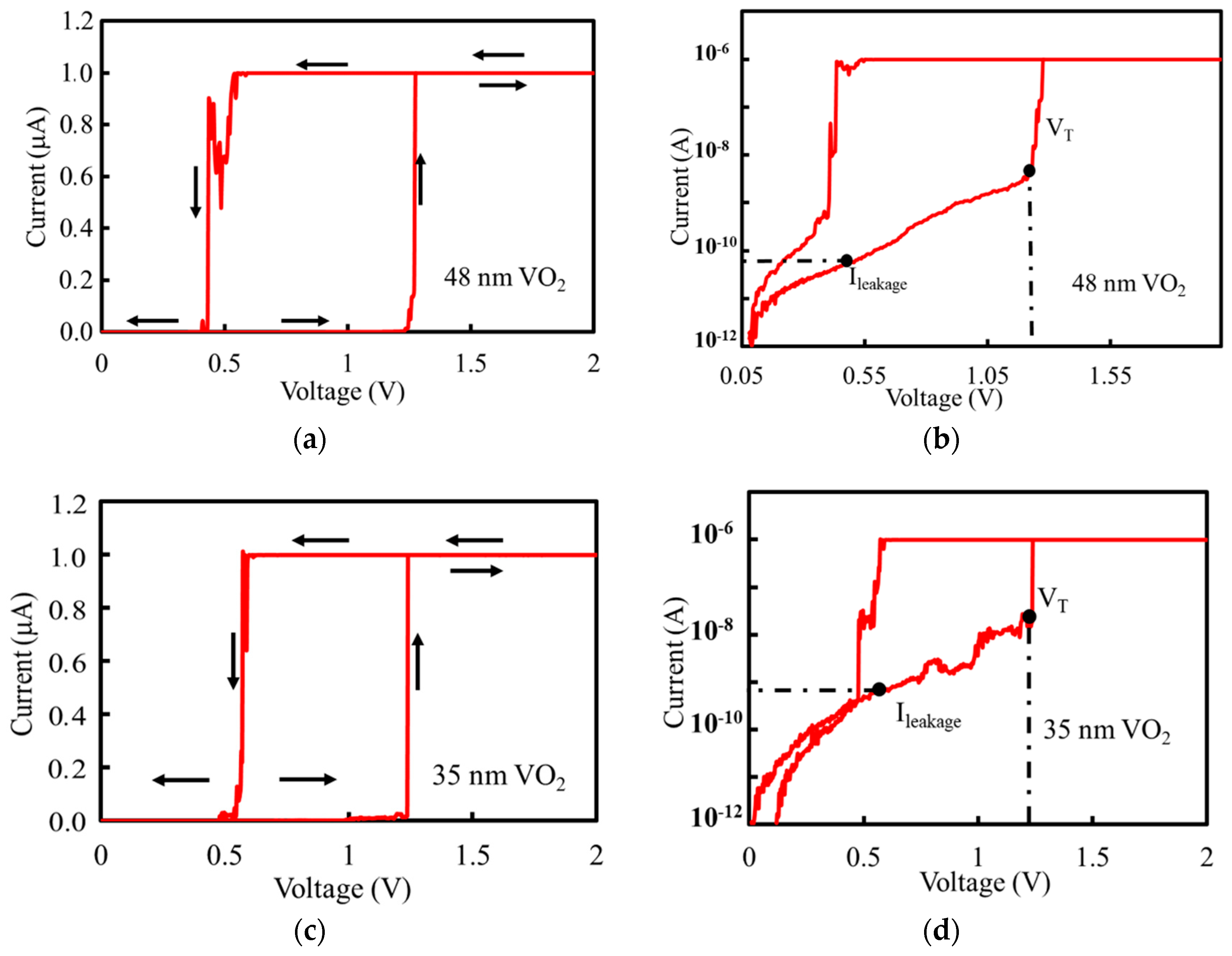
Figure 2 shows I-V measurement results obtained for 48 nm and 35 nm particles. Sharp transitions in I-Vs were observed in the NP-VO2 ranging in size from 13 nm to 53 nm with turn-on voltages (VT) ranging from 0.5–2.0 V. The leakage current and the sub-threshold slopes were calculated for each nano-particle at V = VT/2 and V = VT, respectively, as shown in Figure 2b,d.
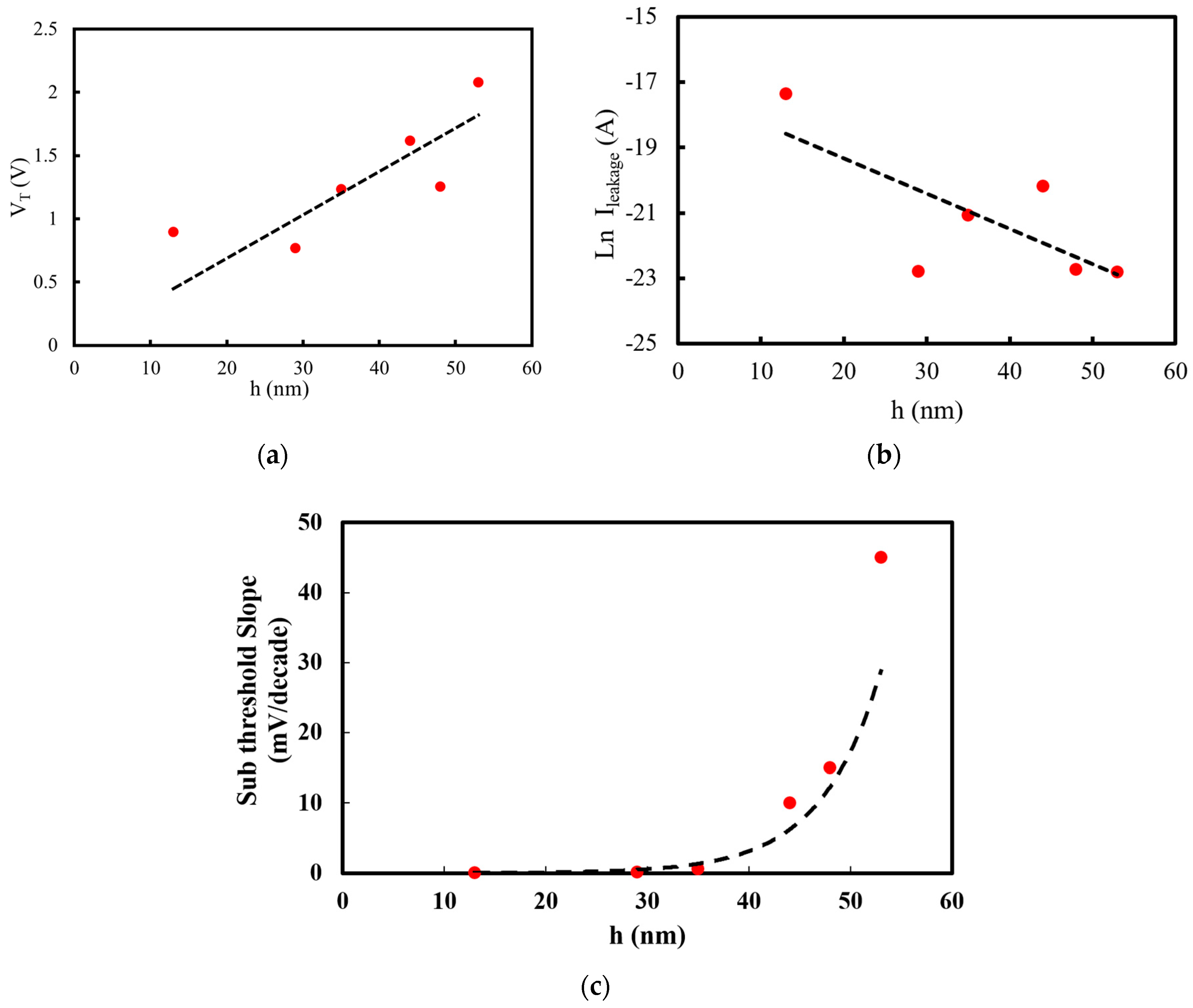
Figure 3a shows VT (defined in Figure 2) as a function of the particle size. Assuming that VT = 0 V for h = 0 nm, the scattered data tentatively fits a line given by VT (V) = 0.034 h with “h” in nm. Therefore, the critical transition field (Ec = VT/h) is Ec ~ 3.44 × 10⁵ V/cm. The leakage current as a function of particle size is shown in Figure 3b and has an approximate dependence given by Ileakage(A) = 3.4 × 10⁻⁸e−h/9.1. This indicates an asymptotic leakage current of 34 nA at zero particle size and tunneling (carrier) decay constant of 9.1 nm inside the NP-VO2.
Next, we examined the slope of the I-V at VT/2 (see Figure 2b). This slope can be viewed as the switching current slope denoted by Sc. Sc increased as a function of particle size and was approximately given by Sc (mV/decade) = 2.1 × 10⁻³eh/6 as shown in Figure 3c and was around 0.6 mV/decade for particle size of 34 nm. The slope of I-V curve indicated by Sc is different than the slope of the MOVFET IDS versus VG curve indicated by St. The exponential dependence of Sc on particle size indicates that as the particle size becomes larger, the conduction tunnel paths and energies through the particle become more numerous leading to shallower I-V switching curve.
3. Device Studies
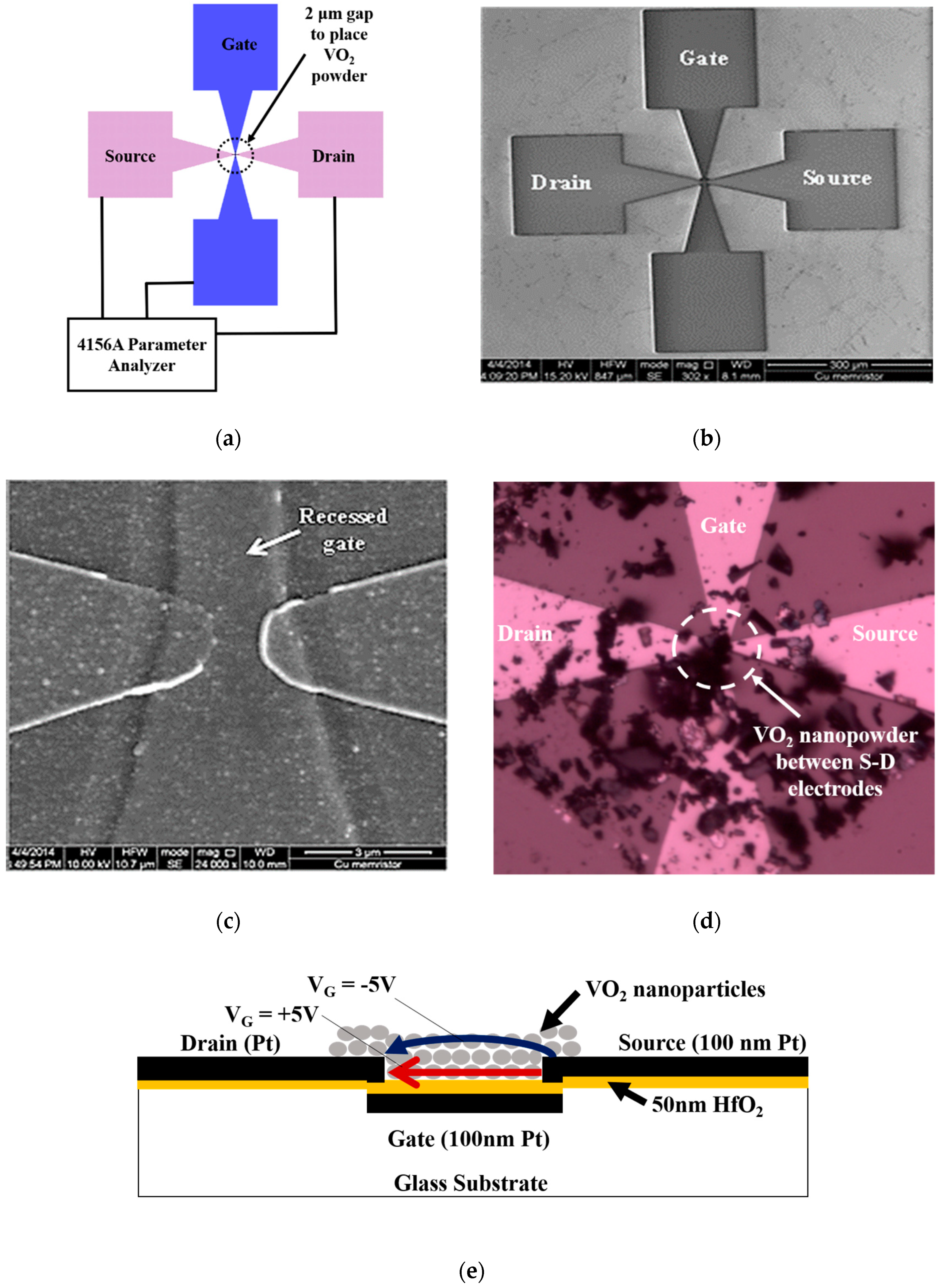
We next incorporated the NP-VO2 in the channel of an FET that were fabricated on a glass substrate with a 100 nm Pt gate covered by a 50 nm atomic layer deposited (ALD) HfO2 dielectric and a 100 nm Pt drain and source electrodes, as shown in Figure 4a,b. The fabrication process is discussed in [14] and was started with etching a 4” glass substrate by immersing it in buffered oxide etch (BOE) for 1 min to create 100 nm deep trenches for the gate metallization regions. After 100 nm Pt gate metal deposition and patterning, 50 nm-thick HfO2 was deposited using atomic layer deposition technique as gate oxide. 100 nm of Pt was then sputter deposited and patterned to create the source-drain regions. Figure 4b,c show the SEM image of the fabricated open-channel FET device.
The open-channel device geometry enables any material to be deposited in the channel region of the FET. To form the NP-VO2 channel, we mixed the VO2 powder with n-butyl-acetate and a small amount of silver paint (1% to 10% in weight) and then ultrasonicated the mixture that was subsequently deposited using a fine brush in the MOVFET’s channel region, as shown in Figure 4d.
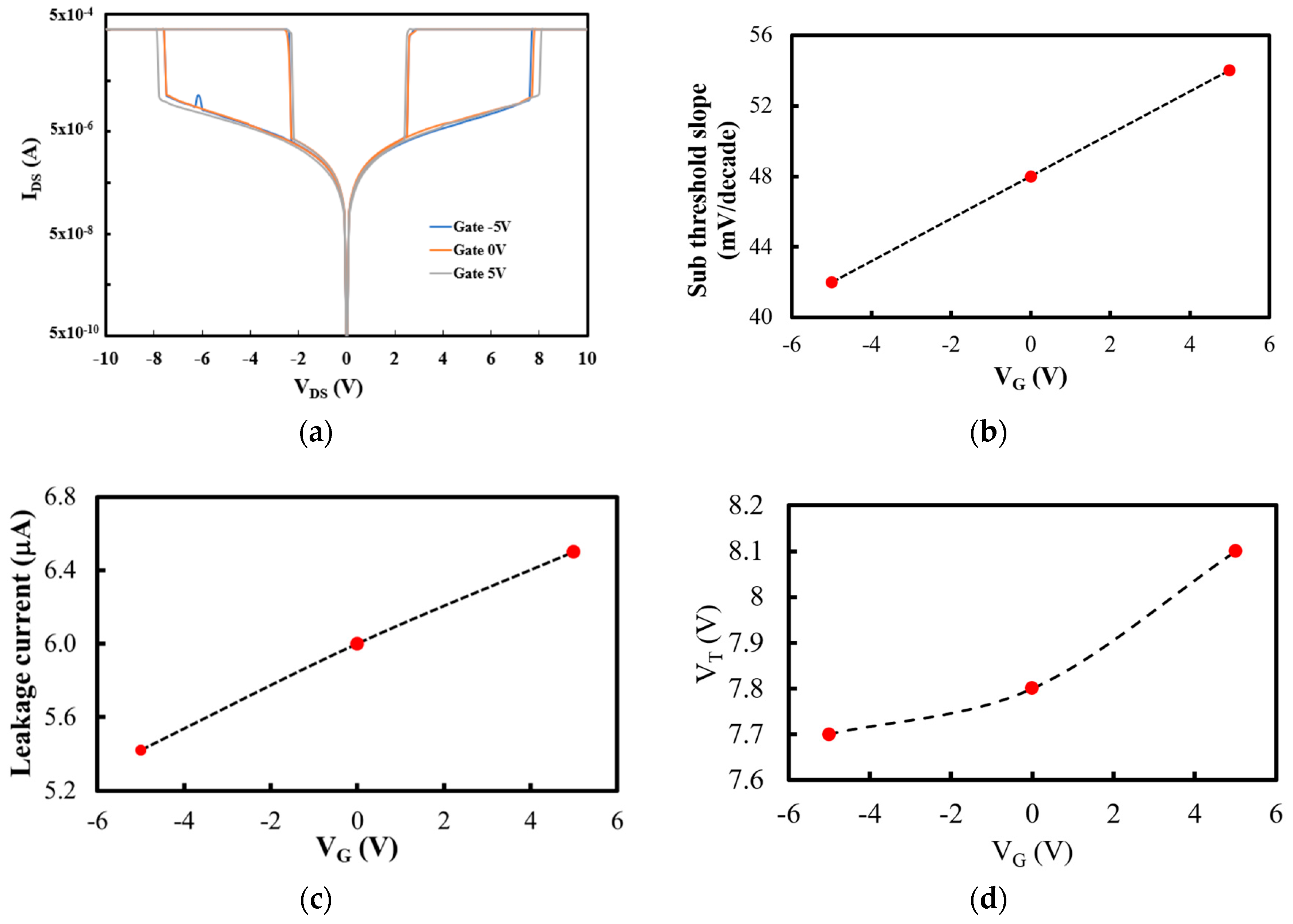
Figure 5a shows a typical IDS-VDS characteristic of the MOVFET. The transition from insulator to metal results in the very sharp increase in the IDS as a function of increasing VDS. IDS transitions for decreasing VDS are also very sharp. In these experiments the IDS was limited to 0.5 mA by the instrument to prevent device breakdown. The IDS-ON/IDS-OFF in these devices, measured using pulsed voltages, were higher than 1000, but we limited the current in static measurements. Figure 5b shows the sub-threshold current as a function of VG. The sub-threshold slope increased as a function of gate voltage. Figure 5c shows the IDS at VT/2 (= Ileakage) as a function of VG, clearly indicating that the leakage current is lower at the negative gate voltages compared to zero and positive gate voltages. We also note that positive gate voltages increased the VT (Figure 5d), while the negative gate voltage reduced it. The VDS voltage step in these experiments was 100 mV.
4. Discussion
The main charge carriers in VO2 are believed to be electrons [2,15]. It is also assumed that the IMT is triggered by the onset of a critical density of electrons in the channel [2,16]. Thus, one expects the threshold voltage in the MOVFET to become smaller at more positive gate voltages. However, we note that just the opposite is observed in Figure 5c. We also note in Figure 3a that in nano-particles, the transition voltage became smaller in smaller particles. Putting these two observations together, we conclude that the gate electric field in our MOVFET changes the current path between the drain and source, as schematically shown by the white and gray (red) arrows in Figure 4e. When the gate voltage is positive, the conduction path is much wider than when the gate voltage is negative. A negative gate voltage “pushes” the conduction path away from the channel‒gate interface region and confines it to a thinner layer at the top. Thus, the conduction occurs over the smaller channel cross section. The VG dependence of all other parameters (St, Sc and Ileakage) agree with this observation.
We also note that other groups working with single crystal thin-film VO2 reported difficulty demonstrating gate field effect [17]. This is attributed to the presence of high carrier (electron) concentration ~1018–1021 cm−3 [7] in the insulator phase of the VO2 that is difficult to modulate and requires very high breakdown gate insulator material. In our devices, we used NP-VO2 that also show the same levels of electron concentrations as calculated from the leakage currents of Figure 2. However, nano-particles couple to each other through their outer boundary layers with lower electron concentrations. The relatively weak coupling between NP-VO2 enables the gate field effect to modulate the current path that gives rise to the modulation of the VT, Ileakage, and St.
While the exact origin of the field-effect induced IMT is still under investigation, it is believed to be non-thermal. Very fast switching (10 ns) in optimized two-terminal devices with thin-film VO2 active regions is also reported [18] indicating the possibility of non-thermal switching mechanisms in these materials.
5. Conclusions
The current-induced IMT in NP-VO2 was investigated using cAFM measurements. The transition voltage in NP-VO2 decreased while the leakage current increased as a function of the particle size. These measurements were followed by construction of NP-VO2 FET devices and the related IDS-VDS/VG measurements. We used open-channel FET devices and drop-casted NP-VO2 to form their channels and measured the resulting MOVFET characteristics that showed gate voltage dependent IDS-VDS.
Author Contributions
Investigation, R.L.; Original Idea and Supervision, M.T.-A.
Funding
This research was funded by the Utah Science and Technology and Research Program.
Conflicts of Interest
The authors declare no conflict of interest.
References
- Tan, X.; Yao, T.; Long, R.; Sun, Z.; Feng, Y.; Cheng, H.; Wei, S. Unraveling metal-insulator transition mechanism of VO2 triggered by tungsten doping. Sci. Rep. 2012, 2, 466. [Google Scholar] [CrossRef] [PubMed]
- Stefanovich, G.; Pergament, A.; Stefanovich, D. Electrical switching and Mott transition in VO2. J. Phys. Condens. Matter 2000, 12, 8837. [Google Scholar] [CrossRef]
- Zylbersztejn, A.; Mott, N.F. Metal-insulator transition in vanadium dioxide. Phys. Rev. B 1975, 11, 4383. [Google Scholar] [CrossRef]
- Lee, S.H.; Kim, M.K.; Lee, J.W.; Yang, Z.; Ramanathan, S.; Tiwari, S. Vanadium dioxide (VO2) is also a ferroelectric: Properties from memory structures. In Proceedings of the 11th IEEE Conference on Nanotechnology (IEEE-NANO), Portland, OR, USA, 15–18 August 2011; pp. 735–739. [Google Scholar]
- Nakano, M.; Shibuya, K.; Okuyama, D.; Hatano, T.; Ono, S.; Kawasaki, M.; Iwasa, Y.; Tokura, Y. Collective bulk carrier delocalization driven by electrostatic surface charge accumulation. Nature 2012, 487, 459–462. [Google Scholar] [CrossRef] [PubMed]
- Wei, J.; Wang, Z.; Chen, W.; Cobden, D.H. New aspects of the metal–insulator transition in single-domain vanadium dioxide nanobeams. Nat. Nanotechnol. 2009, 4, 420–424. [Google Scholar] [CrossRef] [PubMed] [Green Version]
- Jin, F.; Tabib-Azar, M. Optical Tweezer Assembled VO2 Particles Aligned by Drain-Source Bowtie Antenna MOSFET with 10 mV/dec Sub-Threshold Slopes. Electron Devices Lett. 2019. under review. [Google Scholar]
- Oliva, N.; Casu, E.A.; Yan, C.; Krammer, A.; Magrez, A.; Schueler, A.; Martin, O.; Ionescu, M.A. MoS2/VO2 vdW Heterojunction Devices: Tunable Rectifiers, Photodiodes and Field Effect Transistors. Available online: https://infoscience.epfl.ch/record/253434 (accessed on 12 December 2018).
- Chen, C.-K.; Lin, C.-Y.; Chen, P.-H.; Chang, T.-C.; Shih, C.-C.; Tseng, Y.-T.; Zheng, H.-X.; Chen, Y.-C.; Chang, Y.-F.; Lin, C.-C.; et al. The Demonstration of Increased Selectivity during Experimental Measurement in Filament-Type Vanadium Oxide-Based Selector. IEEE Trans. Electron Devices 2018, 99, 1–6. [Google Scholar] [CrossRef]
- Vitale, A.; Casu, E.A.; Biswas, A.; Rosca, T.; Alper, C.; Krammer, A.; Luong, G.V.; Zhao, Q.-T.; Mantl, S.; Schuler, A.; et al. A Steep-Slope Transistor Combining Phase Change and Band-to-Band Tunneling to Achieve a sub-Unity Body Factor. Sci. Rep. 2017, 7, 355. [Google Scholar] [CrossRef] [PubMed]
- Wang, C.Q.; Shao, J.; Liu, X.L.; Chen, Y.; Xiong, W.M.; Zhang, X.Y.; Zheng, Y. Phase Transition Characteristics in the Conductivity of VO2(A) nanowires: Size and Surface Effects. Phys. Chem. C 2016, 18, 10262. [Google Scholar] [CrossRef] [PubMed]
- Yethiraj, M.; Werner, S.A.; Yelon, W.B.; Honig, J.M. Phase transitions in pure and Cr-doped V2O3. Phys. B+C 1986, 136, 458–460. [Google Scholar] [CrossRef]
- Strem Chemicals. Available online: http://www.strem.com/catalog/v/93-2309/80/vanadium_12036-21-4 (accessed on 12 December 2018).
- Mou, N.I.; Zhang, Y.; Pai, P.; Tabib-Azar, M. Steep Sub-threshold Current Slope (~2mV/dec) Pt/Cu2S/Pt Gated Memristor with lon/Ioff>100. Solid-State Electron. 2017, 127, 20–25. [Google Scholar] [CrossRef]
- Duchene, J.; Terraillon, M.; Pailly, P.; Adam, G. Filamentary Conduction in VO2 Coplanar Thin-Film Devices. Appl. Phys. Lett. 1971, 19, 115. [Google Scholar] [CrossRef]
- Okimura, K.; Ezreena, N.; Sasakawa, Y.; Sakai, J. Electric Field-Induced Multi-Step Resistance Switching Phenomena in a Planer VO2/c-Al2O3 Structure. Jpn. J. Appl. Phys. 2009, 48, 065003. [Google Scholar] [CrossRef]
- Kim, H.T.; Chae, B.G.; Youn, D.H.; Kim, G.; Kang, K.Y.; Lee, S.J.; Kim, K.; Lim, Y.S. Raman study of electric-field-induced first-order metal-insulator transition in VO2-based devices. Appl. Phys. Lett. 2005, 86, 242101. [Google Scholar] [CrossRef] [Green Version]
- Kim, H.T.; Lee, Y.W.; Kim, B.J.; Chae, B.G.; Yun, S.J.; Kang, K.Y.; Lim, Y.S. Monoclinic and correlated metal phase in VO2 as evidence of the Mott transition: Coherent phonon analysis. Phys. Rev. Lett. 2006, 97, 266401. [Google Scholar] [CrossRef] [PubMed]
Figure 1.
Schematic of AFM setup for scanning NP-VO2 over gold covered silicon substrate. (a) AFM setup modified for imaging as well as current-voltage (I-V) measurement using Pt tip. (b) AFM scan showing some of the NP-VO2 where I-V relationships were calculated. (c) Different particle heights ranging from 29 nm–44 nm are seen in the above image. (d) Section scan showing the lateral profile of NP-VO2 with a height of 44nm.


Figure 2.
Representative current versus voltage (I-V) measurement results between the Pt AFM probe tip and NP-VO2 on gold. (a) I-V of a 48 nm VO2 particle and (b) the same I-V in log scale clearly showing VT and Ileakage at VT/2. (c) I-V of a 35 nm VO2 particle and (d) its log scale.
Figure 2.
Representative current versus voltage (I-V) measurement results between the Pt AFM probe tip and NP-VO2 on gold. (a) I-V of a 48 nm VO2 particle and (b) the same I-V in log scale clearly showing VT and Ileakage at VT/2. (c) I-V of a 35 nm VO2 particle and (d) its log scale.

Figure 3.
(a) VT, (b) Ileakage and (c) switching current slope (Sc) as a function of VO2 nanoparticle size. The values of VT and leakage currents were taken from the I-V curves of Figure 2.
Figure 3.
(a) VT, (b) Ileakage and (c) switching current slope (Sc) as a function of VO2 nanoparticle size. The values of VT and leakage currents were taken from the I-V curves of Figure 2.

Figure 4.
(a) VO2 MOSFET was connected to a semiconductor parameter analyzer to obtain its electrical characteristics. (b) and (c) SEM images of the open-face MOSFET used in our experiments [14]. (d) Optical image of the open-face MOSFET with drop-cast NP-VO2. Schematic cross-section view of the VO2 MOSFET device architecture with gate embedded inside a glass wafer. (e) Schematic of the cross section of the open-face MOSFET with VO2 channel showing the control of the conduction path using the gate field effect.

Figure 5.
(a) NP-VO2 MOSFET characteristics at room temperature. The current was limited to 0.5 mA, and the VDS voltage steps was 100 mV. (b) Sub-threshold slope (St) of the IDS versus VG. (c) Leakage current as a function of VG. (d) Threshold voltage as a function of gate voltage.
Figure 5.
(a) NP-VO2 MOSFET characteristics at room temperature. The current was limited to 0.5 mA, and the VDS voltage steps was 100 mV. (b) Sub-threshold slope (St) of the IDS versus VG. (c) Leakage current as a function of VG. (d) Threshold voltage as a function of gate voltage.

© 2019 by the authors. Licensee MDPI, Basel, Switzerland. This article is an open access article distributed under the terms and conditions of the Creative Commons Attribution (CC BY) license (http://creativecommons.org/licenses/by/4.0/).
Share and Cite
MDPI and ACS Style
Tabib-Azar, M.; Likhite, R. Nano-Particle VO2 Insulator-Metal Transition Field-Effect Switch with 42 mV/decade Sub-Threshold Slope. Electronics 2019, 8, 151. https://doi.org/10.3390/electronics8020151
AMA Style
Tabib-Azar M, Likhite R. Nano-Particle VO2 Insulator-Metal Transition Field-Effect Switch with 42 mV/decade Sub-Threshold Slope. Electronics. 2019; 8(2):151. https://doi.org/10.3390/electronics8020151
Chicago/Turabian StyleTabib-Azar, Massood, and Rugved Likhite. 2019. "Nano-Particle VO2 Insulator-Metal Transition Field-Effect Switch with 42 mV/decade Sub-Threshold Slope" Electronics 8, no. 2: 151. https://doi.org/10.3390/electronics8020151
Note that from the first issue of 2016, this journal uses article numbers instead of page numbers. See further details here.