Optimal Physical Implementation of Radiation Tolerant High-Speed Digital Integrated Circuits in Deep-Submicron Technologies

Abstract
:1. Introduction
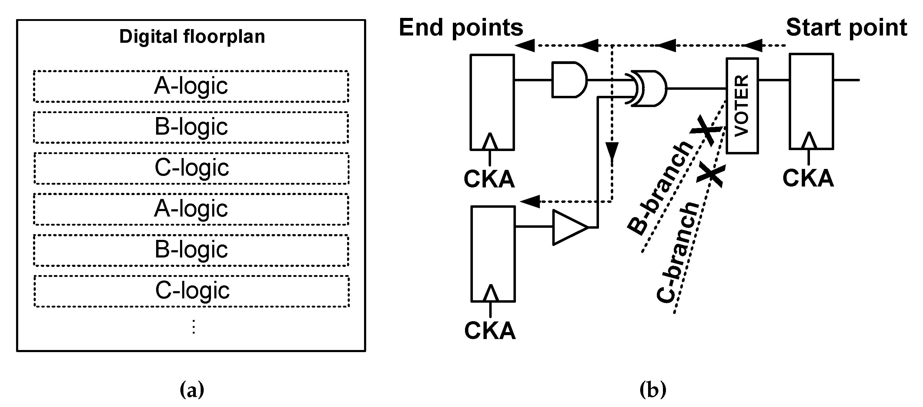
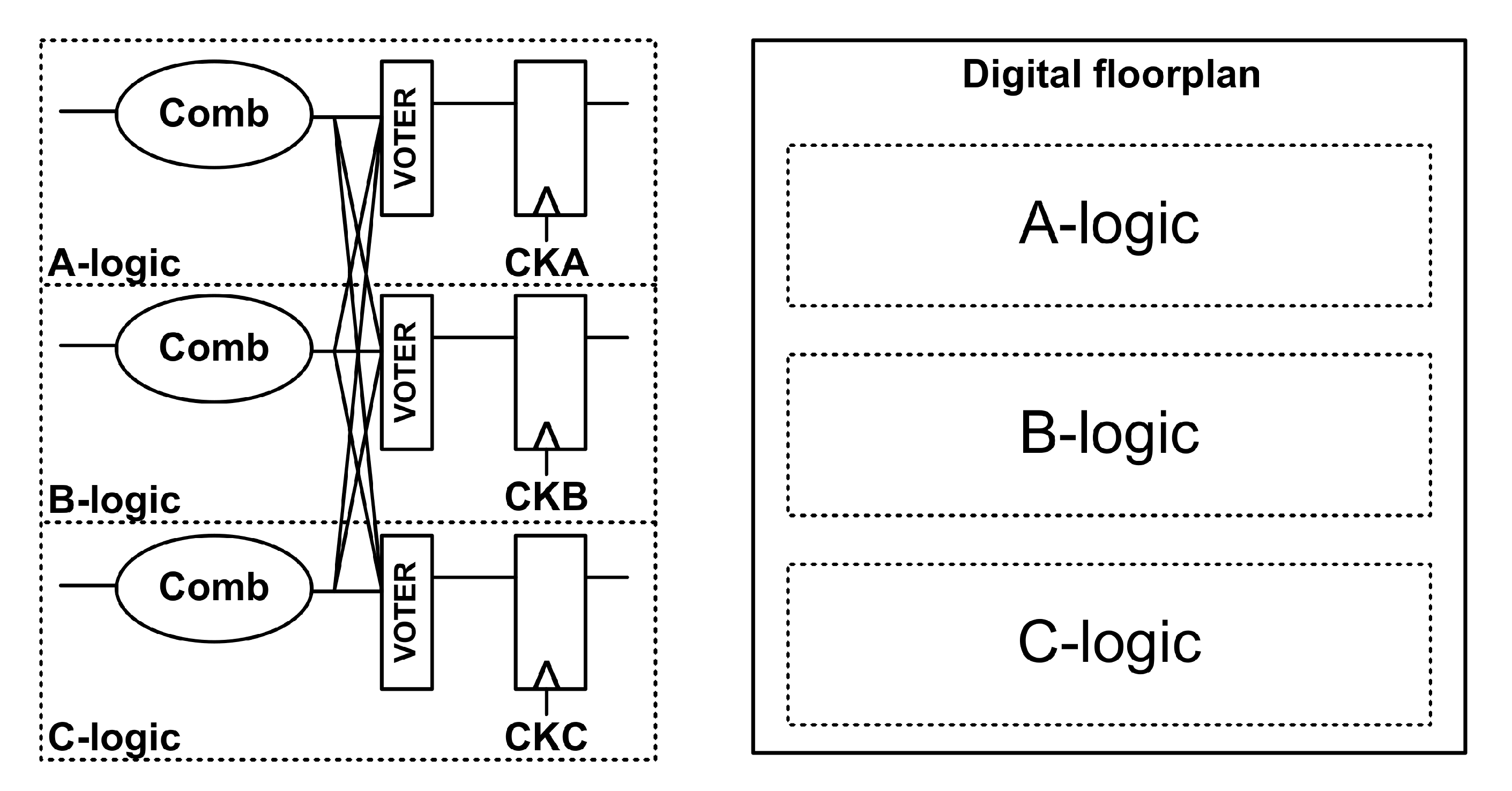
2. Physical Implementation for TMR Circuits
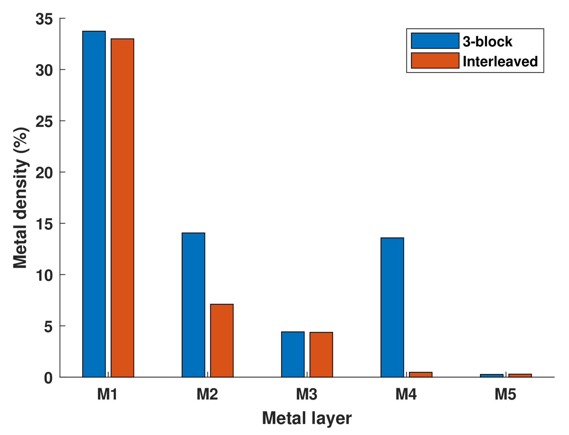
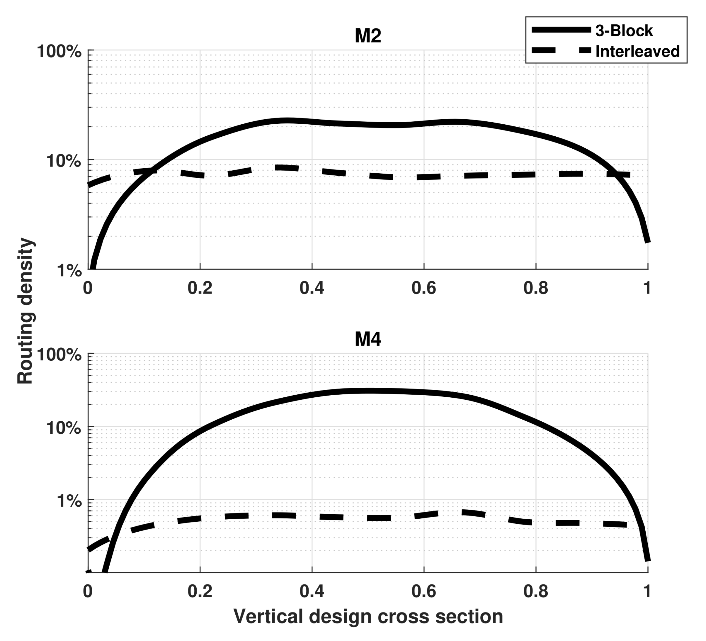
2.1. Conventional 3-Block Approach
2.2. Novel Interleaved Approach
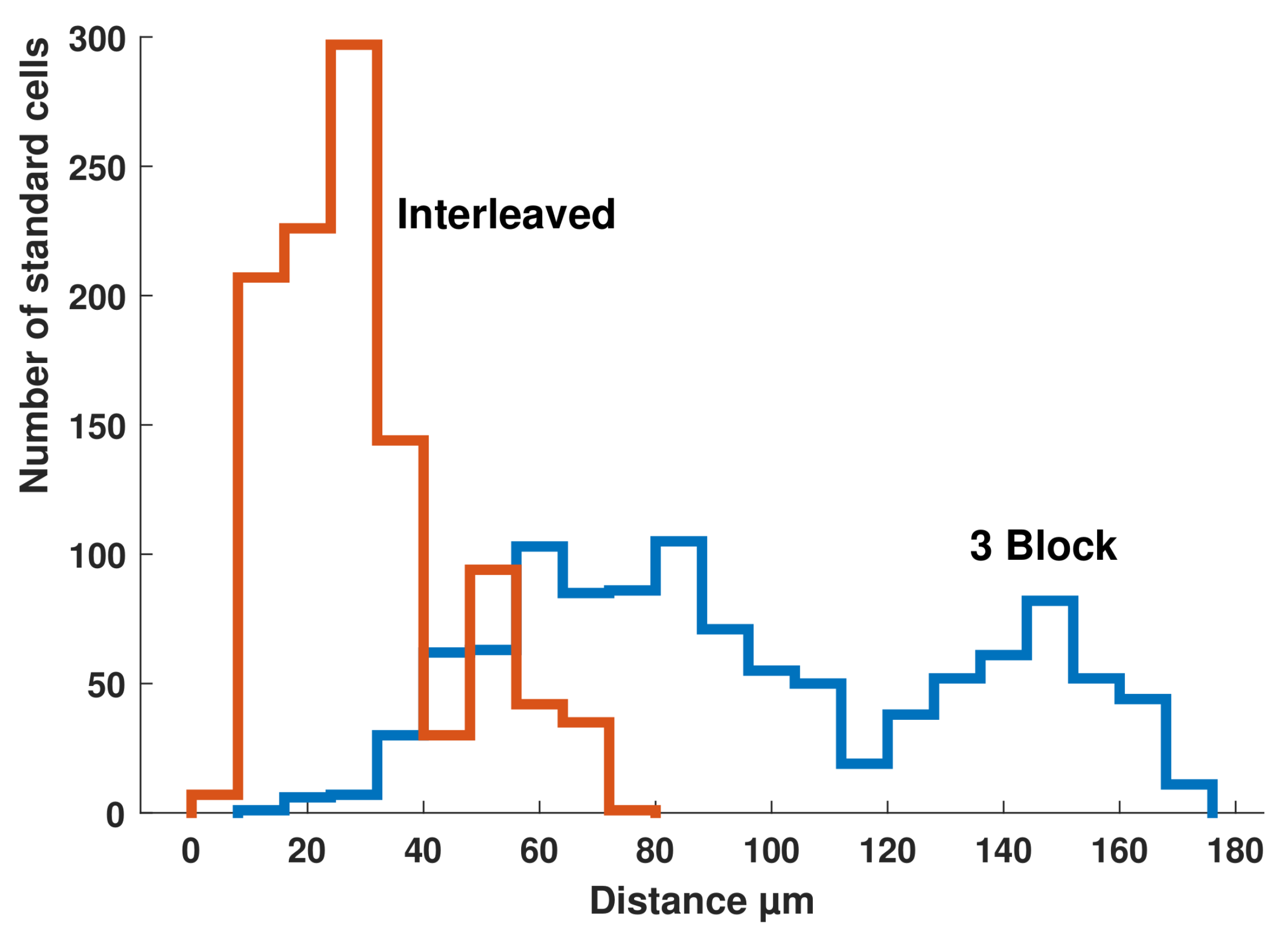
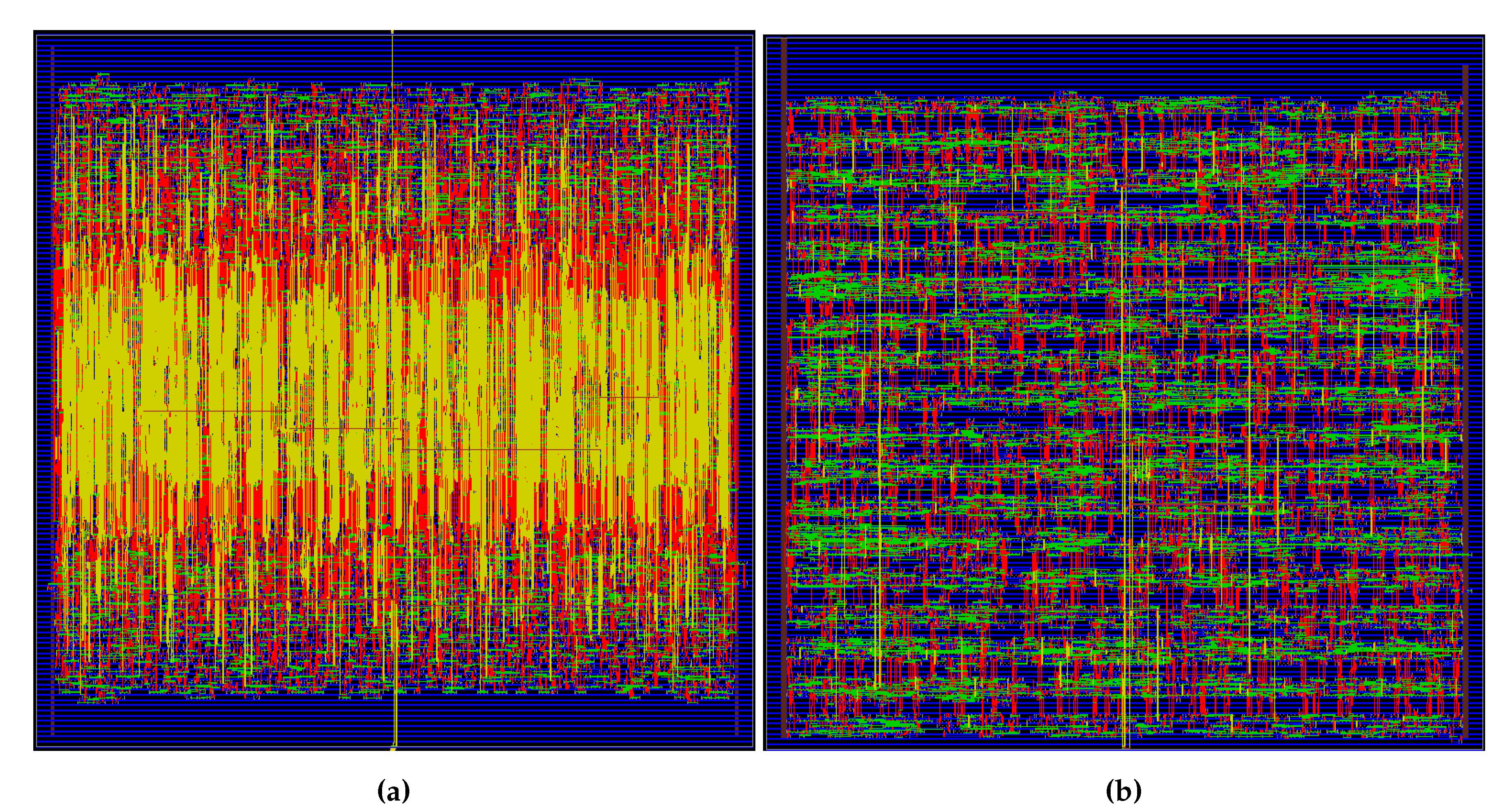
3. Simulated Performance Analysis
4. Conclusions
Author Contributions
Funding
Conflicts of Interest
References
- Harrington, R.C.; Kauppila, J.S.; Warren, K.M.; Chen, Y.P.; Maharrey, J.A.; Haeffner, T.D.; Loveless, T.D.; Bhuva, B.L.; Bounasser, M.; Lilja, K.; et al. Estimating Single-Event Logic Cross Sections in Advanced Technologie. IEEE Trans. Nucl. Sci. 2017, 64, 2115–2121. [Google Scholar]
- Nsengiyumva, P.; Ball, D.R.; Kauppila, J.S.; Tam, N.; McCurdy, M.; Holman, W.T.; Alles, M.L.; Bhuva, B.L.; Massengill, L.W. A Comparison of the SEU Response of Planar and FinFET D Flip-Flops at Advanced Technology Nodes. IEEE Trans. Nucl. Sci. 2016, 63, 266–272. [Google Scholar] [CrossRef]
- Chen, C.-H.; Knag, P.; Zhang, Z. Characterization of Heavy-Ion-Induced Single-Event Effects in 65 Nm Bulk CMOS ASIC Test Chips. IEEE Trans. Nucl. Sci. 2014, 61, 2694–2701. [Google Scholar] [CrossRef]
- Benedetto, J.; Eaton, P.; Avery, K.; Mavis, D.; Gadlage, M.; Turflinger, T.; Dodd, P.E.; Vizkelethyd, G. Heavy ion-induced digital single-event transients in deep submicron Processes. IEEE Trans. Nucl. Sci. 2004, 51, 3480–3485. [Google Scholar] [CrossRef]
- Benedetto, J.M.; Eaton, P.H.; Mavis, D.G.; Gadlage, M.; Turflinger, T. Digital Single Event Transient Trends With Technology Node Scaling. IEEE Trans. Nucl. Sci. 2006, 53, 3462–3465. [Google Scholar] [CrossRef]
- Dodd, P.E.; Shaneyfelt, M.R.; Felix, J.A.; Schwank, J.R. Production and propagation of single-event transients in high-speed digital logic ICs. IEEE Trans. Nucl. Sci. 2004, 51, 3278–3284. [Google Scholar] [CrossRef]
- Chen, R.M.; Diggins, Z.J.; Mahatme, N.N.; Wang, L.; Zhang, E.X.; Chen, Y.P.; Liu, Y.N.; Narasimham, B.; Witulski, A.F.; Bhuva, B.L. Analysis of temporal masking effect on single-event upset rates for sequential circuits. In Proceedings of the 2016 16th European Conference on Radiation and Its Effects on Components and Systems (RADECS), Bremen, Germany, 19–23 September 2016. [Google Scholar] [CrossRef]
- Reed, R.A.; Carts, M.A.; Marshall, P.W.; Marshall, C.J.; Buchner, S.; La Macchia, M.; Mathes, B.; McMorrow, D. Single Event Upset cross sections at various data rates. IEEE Trans. Nucl. Sci. 1996, 43, 2862–2867. [Google Scholar] [CrossRef]
- Ruano, O.; Reviriego, P.; Maestro, J.A. Automatic insertion of selective TMR for SEU mitigation. In Proceedings of the RADECS, Gothenburg, Sweden, 16–21 September 2018; pp. 284–287. [Google Scholar]
- Evans, A.; Glorieux, M.; Alexandrescu, D.; Polo, C.B.; Ferlet-Cavrois, V. Single event multiple transient (SEMT) measurements in 65 nm bulk technology. In Proceedings of the 2016 16th European Conference on Radiation and Its Effects on Components and Systems (RADECS), Bremen, Germany, 19–23 September 2016. [Google Scholar] [CrossRef]
- Zhang, H.; Jiang, H.; Assis, T.R.; Ball, D.R.; Narasimham, B.; Anvar, A.; Massengill, L.W.; Bhuva, B.L. Angular Effects of Heavy-Ion Strikes on Single-Event Upset Response of Flip-Flop Designs in 16-nm Bulk FinFET Technology. IEEE Trans. Nucl. Sci. 2017, 64, 491–496. [Google Scholar] [CrossRef]
- Bhuva, B.L.; Tam, N.; Massengill, L.W.; Ball, D.; Chatterjee, I.; McCurdy, M.; Alles, M.L. Multi-Cell Soft Errors at Advanced Technology Nodes. IEEE Trans. Nucl. Sci. 2015, 62, 2585–2591. [Google Scholar] [CrossRef]
- Ulloa, G.; Lucena, V.; Meinhardt, C. Comparing 32nm full adder TMR and DTMR architectures. In Proceedings of the 2017 24th IEEE International Conference on Electronics, Circuits and Systems (ICECS), Batumi, Georgia, 5–8 December 2017; pp. 294–297. [Google Scholar]
- Balasubramanian, P.; Prasad, K. A Fault Tolerance Improved Majority Voter for TMR System Architecture. WSEAS Trans. Circuits Syst. 2016, 15, 108–122. [Google Scholar]
- Shinohara, K.; Watanabe, M. A double or triple module redundancy model exploiting dynamic reconfigurations. In Proceedings of the 2008 NASA/ESA Conference on Adaptive Hardware and Systems, Noordwijk, The Netherlands, 22–25 June 2008; pp. 114–121. [Google Scholar]
- Hasanbegovic, A.; Aunet, S. Heavy Ion Characterization of Temporal-, Dual- and Triple Redundant Flip-Flops Across a Wide Supply Voltage Range in a 65 nm Bulk CMOS Process. IEEE Trans. Nucl. Sci. 2016, 63, 2962–2970. [Google Scholar] [CrossRef]
- Schmidt, R.; García-Ortiz, A.; Fey, G. Temporal redundancy latch-based architecture for soft error mitigation. In Proceedings of the 2017 IEEE 23rd International Symposium on On-Line Testing and Robust System Design (IOLTS), Thessaloniki, Greece, 3–5 July 2017; pp. 240–243. [Google Scholar]
- She, X.; McElvain, K.S. Time multiplexed triple modular redundancy for single event upset mitigation. IEEE Trans. Nucl. Sci. 2009, 56, 2443–2449. [Google Scholar] [CrossRef]
- Tooba, A.; Abdus Sami, H.; Hossein, M.; Jeong, A.L. Input vulnerability-aware approximate triple modular redundancy: Higher fault coverage, improved search space, and reduced area overhead. Electron. Lett. 2018, 54, 934–936. [Google Scholar]
- She, X.; Li, N. Reducing Critical Configuration Bits via Partial TMR for SEU Mitigation in FPGAs. IEEE Trans. Nucl. Sci. 2017, 64, 2626–2632. [Google Scholar] [CrossRef]
- Matush, B.I.; Mozdzen, T.J.; Clark, L.T.; Knudsen, J.E. Area-Efficient Temporally Hardened by Design Flip-Flop Circuits. IEEE Trans. Nucl. Sci. 2010, 57, 3588–3595. [Google Scholar] [CrossRef]
- Nagpal, C.; Garg, R.; Khatri, S.P. A delay-efficient radiation-hard digital design approach using CSWP elements. In Proceedings of the 2008 Design, Automation and Test in Europe, Munich, Germany, 10–14 March 2008; pp. 345–359. [Google Scholar]
- Kulis, S. Single Event Effects Mitigation with TMRG Tool. J. Instrum. 2017, 12. [Google Scholar] [CrossRef]


| Counter Size | Clock Constraint | Inst. Count | Design Width | |
|---|---|---|---|---|
| Design 1 | 8 × 8 bit | 1.2 ns | 2808 | 175 m |
| Design 2 | 8 × 16 bit | 1.7 ns | 4560 | 250 m |
| Design 3 | 8 × 32 bit | 1.9 ns | 9120 | 350 m |
| (a) 8 × 8 bit | |||
| 3-Block | Interleaved | Difference | |
| Internal power | 20.59 mW | 19.46 mW | −5.4% |
| Switching power | 10.55 mW | 8.712 mW | −17.42% |
| Total Power | 31.14 mW | 28.18 mW | −9.51% |
| Total capacitance | 32 pF | 26 pF | −14.8% |
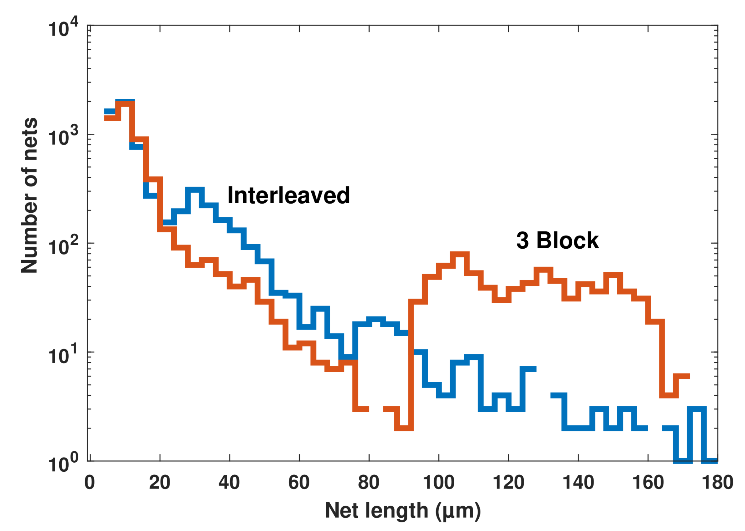
| Total net length | 74,425 m | 47,436 m | −36.26% |
| Average net length | 17 m | 11 m | −35.46% |
| (b) 8 × 16 bit | |||
| 3-Block | Interleaved | Difference | |
| Internal power | 21.95 mW | 22.58 mW | +2.8% |
| Switching power | 11.67 mW | 9.224 mW | −20.95% |
| Total Power | 33.62 mW | 31.8 mW | −5.41% |
| Total capacitance | 45 pF | 38 pF | −15.3% |
| Total net length | 142,468 m | 89,096 m | −37.46% |
| Average net length | 23.9 m | 14.2 m | −40.47% |
| (c) 8 × 32 bit | |||
| 3-Block | Interleaved | Difference | |
| Internal power | 55.17 mW | 51.96 mW | −5.82% |
| Switching power | 34.82 mW | 18.26 mW | −47.55% |
| Total Power | 89.99 mW | 70.22 mW | −21.96% |
| Total capacitance | 108 pF | 60 pF | −44.28% |
| Total net length | 368,032 m | 128,320 m | −65.13% |
| Average net length | 26.8 m | 9.1 m | −65.89% |
© 2019 by the authors. Licensee MDPI, Basel, Switzerland. This article is an open access article distributed under the terms and conditions of the Creative Commons Attribution (CC BY) license (http://creativecommons.org/licenses/by/4.0/).
Share and Cite
Prinzie, J.; Appels, K.; Kulis, S. Optimal Physical Implementation of Radiation Tolerant High-Speed Digital Integrated Circuits in Deep-Submicron Technologies. Electronics 2019, 8, 432. https://doi.org/10.3390/electronics8040432
Prinzie J, Appels K, Kulis S. Optimal Physical Implementation of Radiation Tolerant High-Speed Digital Integrated Circuits in Deep-Submicron Technologies. Electronics. 2019; 8(4):432. https://doi.org/10.3390/electronics8040432
Chicago/Turabian StylePrinzie, Jeffrey, Karel Appels, and Szymon Kulis. 2019. "Optimal Physical Implementation of Radiation Tolerant High-Speed Digital Integrated Circuits in Deep-Submicron Technologies" Electronics 8, no. 4: 432. https://doi.org/10.3390/electronics8040432
APA StylePrinzie, J., Appels, K., & Kulis, S. (2019). Optimal Physical Implementation of Radiation Tolerant High-Speed Digital Integrated Circuits in Deep-Submicron Technologies. Electronics, 8(4), 432. https://doi.org/10.3390/electronics8040432