Article

A Novel Modular Radiation Hardening Approach Applied to a Synchronous Buck Converter

1
Department of Electrical and Computer Engineering, Addis Ababa Institute of Technology, Addis Ababa University, Addis Ababa P.O. Box 385, Ethiopia
2
Department of Electrical and Computer Engineering, Institute of Technology, Hawassa University, Hawassa P.O. Box 05, Ethiopia
3
Department of Electrical Engineering (ESAT)–ADVISE, KU Leuven, 3000 Leuven, Belgium
*
Author to whom correspondence should be addressed.
Electronics 2019, 8(5), 513; https://doi.org/10.3390/electronics8050513
Submission received: 15 April 2019 / Revised: 30 April 2019 / Accepted: 4 May 2019 / Published: 8 May 2019
(This article belongs to the Special Issue Radiation Tolerant Electronics)

Abstract

:
Radiation and extreme temperature are the main inhibitors for the use of electronic devices in space applications. Radiation challenges the normal and stable operation of DC-DC converters, used as power supply for onboard systems in satellites and spacecrafts. In this situation, special design techniques known as radiation hardening or radiation tolerant designs have to be employed. In this work, a module level design approach for radiation hardening is addressed. A module in this sense is a constituent of a digital controller, which includes an analog to digital converter (ADC), a digital proportional-integral-derivative (PID) controller, and a digital pulse width modulator (DPWM). As a new Radiation Hardening by Design technique (RHBD), a four module redundancy technique is proposed and applied to the digital voltage mode controller driving a synchronous buck converter, which has been implemented as hardware-in-the-loop (HIL) simulation block in MATLAB/Simulink using Xilinx system generator based on the Zynq-7000 development board (ZYBO). The technique is compared, for reliability and hardware resources requirement, with triple modular redundancy (TMR), five modular redundancy (FMR) and the modified triplex–duplex architecture. Furthermore, radiation induced failures are emulated by switching all duplicated modules inputs to different signals, or to ground during simulation. The simulation results show that the proposed technique has 25% and 30%longer expected life compared to TMR and FMR techniques, respectively, and has the lowest hardware resource requirement compared to FMR and the modified triplex–duplex techniques.

1. Introduction

Outer space is full of radiation sources that include solar wind, solar flares, coronal mass ejections, galactic cosmic rays, Van Allen radiation belts, solar particle events, etc. This radiation environment consists of particles such as protons, electrons, neutrons, and heavy ions, [1]. The strike of any of these particles may compromise the normal operation of electronic circuits on board of space systems in this environment. Depending on the type and characteristics of the impinging radiation, different effects, either irreversible or (partially or totally) reversible, may arise. There are two major effects of radiation i.e., total ionizing dose (TID) and single event effect (SEE). TID also called cumulative effect, produce gradual changes in the operational parameters of the devices, which tends to degrade the characteristics of the devices overtime. SEE cause abrupt changes or transient behavior in circuits. Such effects, interfere with space systems’ electronics operation, and, in some cases, threaten the survival of such systems. While TID effects reveal themselves gradually often after years of operation before a complete failure, SEEs don’t. This work considers alleviating the effects of SEE on electronic circuits used for space applications.
Currently, the study of techniques to keep electronic circuits operational in such hostile environment has increased [2], driven by the increasing number of applications of radiation tolerant circuits, such as space missions, satellites, high-energy physics experiments, etc. [3,4]. This paper considers a module level approach for radiation hardening using fault tolerant method.
Fault tolerant methods use redundancy to mask or get around faults in electronic circuits. Redundancy is one of the most important methods to obtain highly reliable systems. Redundancy techniques have the ability to deliver continuous service in the presence of hardware faults by providing redundant hardware components. Redundancy techniques in general are adopting additional hardware components or additional computation time, which are used for fault detection or for fault masking so that the effect of faults is not reflected on the output signal [5]. The most common radiation mitigation techniques are TMR and FMR methods [6,7]. They are highly-efficient but very costly and are used for situations where high reliability is targeted. Reliability is an important quality measure of a fault tolerant system.
Reliability is defined as the probability of not failing in a particular environment for a particular mission time. Suppose a system consists of N identical components. Let S(t) be the number of surviving components at time t, and Q(t) the number of components that failed up to time t. Then the probability of survival of the components also known as the reliability R(t), which is given by:
R ( t ) = S ( t ) N
A measure of failure F(t) is defined as the conditional probability that the system fails by time t referred to us unreliability or failure time distribution:
F ( t ) = Q ( t ) N
Since S(t) + Q(t) = N, therefore:
R ( t ) + F ( t ) = 1         o r       F ( t ) = 1 R ( t )
Since F(t) is a probability, its derivative is a probability distribution function and defined as,
f ( t ) = d F ( t ) d t = d R ( t ) d t
where f(t) shows the probability of failures per unit time.
Now, the failure rate λ is defined as the number of failures per unit time, compared with the number of surviving components.
F a i l u r e   r a t e = T h e   n u m b e r   o f   f a i l u r e   p e r   u n i t   t i m e T h e   n u m b e r   o f   s u r v i v i n g   c o m p o n e n t s                   o r              
λ = 1 R ( t )   × d F ( t ) d t
Using Equation (3), the failure rate can be written as,
λ = 1 R ( t ) × d R ( t ) d t
The expression may be integrated from 0 to time t, by considering at time t = 0, R(t) = 1, and at time t the reliability is R(t), then,
0 t λ d t =   1 R ( t ) d R ( t ) R ( t )
Often λ is assumed to be constant during the useful life of the system. Thus,
λ t = l o g R ( t )               o r                 λ t = l o g R ( t )
This gives,
R ( t ) = e λ t
The mean time to failure (MTTF) for the system is obtained as,
M T T F = 0 R ( t ) d t =   1 λ
Assuming independent and identical modules having reliability of Rm and with λ constant failure rate each, and then using the binomial theorem
B ( r : n , R m ) = ( n r ) R m r ( 1 R m ) n r
The reliability of TMR is given as,
R T M R = P r o b a b i l i t y   o f   a l l   t h r e e   m o d u l e s   a r e   f u n c t i o n i n g        + P r o b a b i l i t y   o f   a n y   t w o   m o d l u e s   a r e   f u n c t i o n i n g
R T M R = B ( 3 : 3 ) + B ( 2 : 3 ) = ( 3 3 ) R m 3 ( 1 R m ) 0 +   ( 3 2 ) R m 2 ( 1 R m ) 1
R T M R = 3 R m 2 2 R m 3 = 3 e 2 λ t       2 e 3 λ t
M T T F T M R = 0 R ( t ) d t =   0 ( 3 e 2 λ t       2 e 3 λ t ) d t = 3 2 λ 2 3 λ =     5 6 λ
For the FMR method:
R 5 M R = B ( 5 : 5 ) + B ( 4 : 5 ) +   B ( 3 : 5 )
R 5 M R = ( 5 5 ) R m 5 ( 1 R m ) 0 +   ( 5 4 ) R m 4 ( 1 R m ) 1 + ( 5 3 ) R m 3 ( 1 R m ) 2
R 5 M R = 10 R m 3 15 R m 4 + 6 R m 5 = 10 e 3 λ t       15 e 4 λ t   + 6 e 5 λ t
M T T F 5 M R = 0 R ( t ) d t =   0 ( 10 e 3 λ t 15 e 4 λ t + 6 e 5 λ t ) d t = 10 3 λ 15 4 λ + 6 5 λ = 47 60 λ

2. Motivation

2.1. The Base Architecture

The proposed method is derived from the architecture presented in [5], which is called triplex–duplex redundancy. In this arrangement there are three primary modules using two duplicate modules each. Thus, a total of six identical modules are computing in parallel, which are grouped in three pairs. The computation result of each pair is compared using a comparator. If the results agree, the output of the comparator participates in the voting. If not, the pair of modules is declared faulty and the switch removes the pair from the system.
The hardware resource requirement is 500% more compared to the simplex system and twice compared to that of TMR technique.

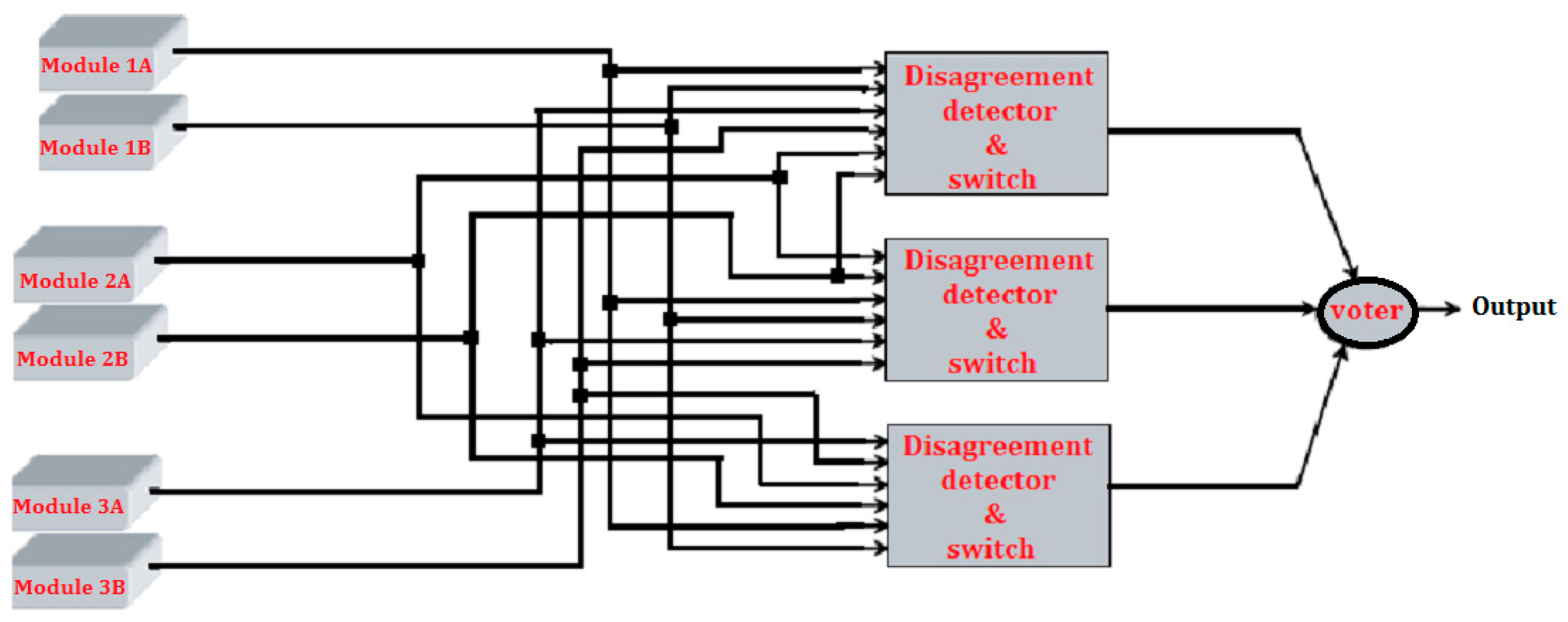
2.2. Modified Triplex–Duplex Architecture

The disadvantage of the triplex–duplex architecture is that it requires two times more hardware resources compared to the TMR method and has the one more module than the FMR method. Both modules in the duplex are removed from the voting as soon as one of the two modules in the duplex fails. This reduces the overall system mean time to failure (MTTF), if no repair is used. Therefore, except for faulty duplex detection, it is similar in operation to TMR.
To increase the reliability of this method, a modified architecture shown in Figure 1 was developed, where the comparator and switch parts are combined and modified in such a way that all duplexes are connected to all disagreement detectors and switch blocks, which allows for any module in the three duplex systems to act as an active spare for any other module in the three duplex systems. Therefore, the overall system will continue to work even if one module in all the three duplexes is failed, or even if only one duplex is left, or two duplexes with one good module each are left. This significantly increases the MTTF of the overall system and helps, if any repair or reconfiguration is used, to reduce the frequency of such repair or reconfiguration compared to TMR or FMR only methods.
This method uses 500% more hardware compared to the simplex system, the same as its base architecture, but with tremendous increase in reliability.
Assuming independent and identical modules having reliability of Rm and with λ constant failure rate each:
R ( t r i p l e x d u p l e x ) m o d   = B ( 6 : 6 ) + B ( 5 : 6 ) +   B ( 4 : 6 ) + B ( 3 : 6 ) +   B ( 2 : 6 )
R ( t r i p l e x d u p l e x ) m o d = ( 6 6 ) R m 6 ( 1 R m ) 0 +   ( 6 5 ) R m 5 ( 1 R m ) 1 + ( 6 4 ) R m 4 ( 1 R m ) 2 +     ( 6 3 ) R m 3 ( 1   R m ) 3 +   ( 6 2 ) R m 2 ( 1 R m ) 4
                    R ( t r i p l e x d u p l e x ) m o d = 15 R m 2 40 R m 3 + 45 R m 4 24 R m 5 + 5 R m 6
                                    = 15 e 2 λ t   40 e 3 λ t   + 45 e 4 λ t 24 e 5 λ t + 5 e 6 λ t
M T T F ( t r i p l e x d u p l e x ) m o d = 0 R ( t ) d t
=   0 ( 15 e 2 λ t 40 e 3 λ t + 45 e 4 λ t 24 e 5 λ t + 5 e 6 λ t ) d t
= 15 2 λ 40 3 λ + 45 4 λ 24 5 λ + 5 6 λ =     87 60 λ
There is 61% and 66% improvement in MTTF compared to TMR and FMR methods, respectively.

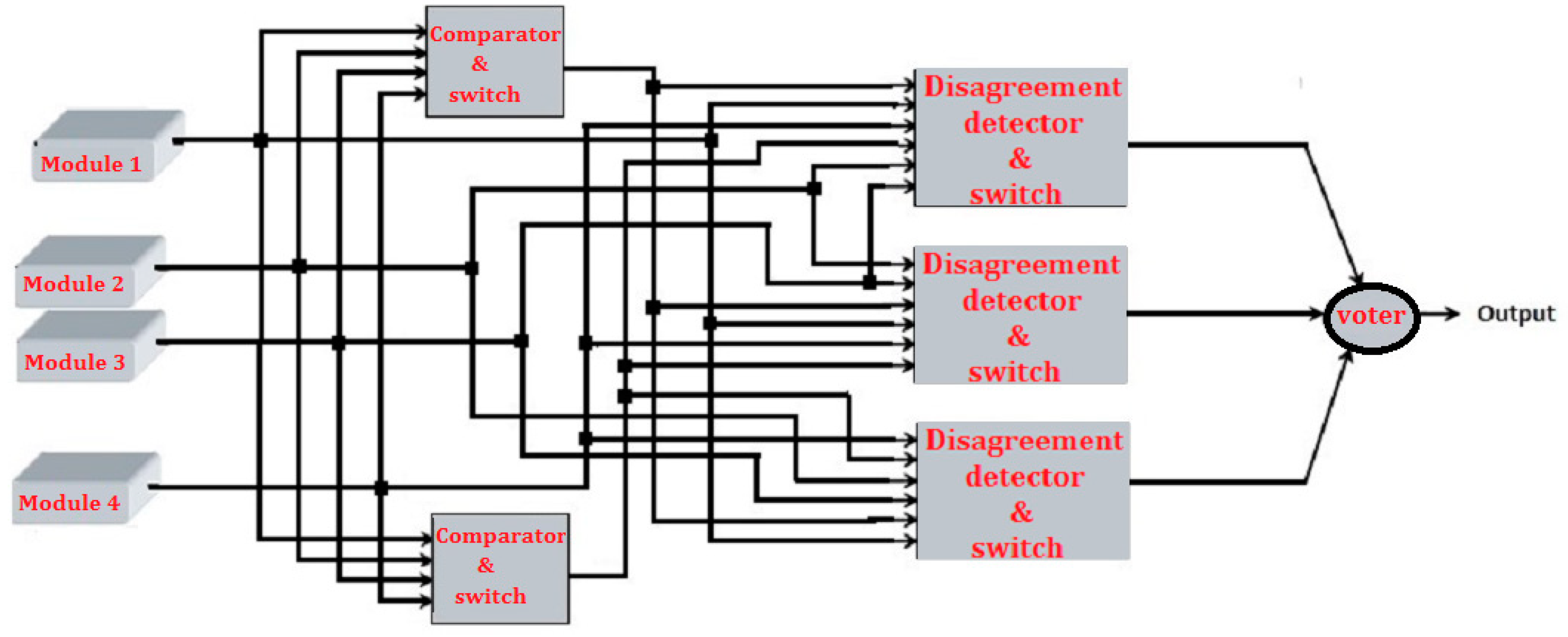
3. Proposed Four Modules Architecture

Besides having the best reliability and consequently MTTF, the disadvantage of the modified triplex–duplex architecture is its high hardware resource utilization. In effort to come up with high reliability and lower resource requirement redundancy, a four module architecture was developed as shown in the Figure 2, which has the highest reliability compared to both TMR and FMR methods and lowest hardware resource requirement compared to FMR and the modified triplex–duplex methods.
The operation of this architecture is similar to the modified triplex–duplex architecture above, except that, there are four physical modules and two clone modules reducing the total number of actual duplicated modules to four instead of six. The clone modules were created as long as at least two of the physical modules were fault free, which in effect significantly reduces hardware resource utilization compared to the FMR and the modified triplex–duplex methods. The architecture masks the failure of two physical modules out of four.
The proposed four modules architecture is comparable, in terms of reliability, to the four modules highly reliable self-purging redundancy, [8,9]. Self-purging redundancy uses a threshold voter instead of a majority voter. A threshold voter outputs a 1, if the number of its inputs that are 1 is greater than or equal to the threshold value; otherwise it outputs a 0. The idea of self-purging redundancy is that if only one module fails, then its output will be different from the others. A switch checks if a module’s output differs from the output of a threshold voter. If it does differ, then the module is assumed to be faulty and its control flip-flop is reset to 0. This permanently masks the output of the module so that its input to the threshold voter will always be 0.
As pointed out in [8], the self-purging method is not so much popular due to its complex threshold voter architecture. In case of the self-purging technique, faulty module detection is performed by comparing each module’s output with the voted output. However, the detection of the faulty module is carried out before voting. In the case of the developed four modules method, it reduces the complexity encountered with a faulty voter especially when using multiple voters in the case of self-purging redundancy. Moreover, the proposed four-module redundancy technique can tolerate the simultaneous failure of two modules, whereas, a four module self-purging redundancy with a threshold of 2 cannot. Self-purging redundancy with a threshold of T can tolerate up-to T-1 simultaneous failures.
Assuming the same conditions as in previous cases for reliability calculation,
R F o u r m o d = B ( 4 : 4 ) + B ( 3 : 4 ) +   B ( 2 : 4 )
R F o u r m o d = ( 4 4 ) R m 4 ( 1 R m ) 0 +   ( 4 3 ) R m 3 ( 1 R m ) 1 + ( 4 2 ) R m 2 ( 1 R m ) 2
R F o u r m o d = 3 R m 4 8 R m 3 + 6 R m 2 = 3 e 4 λ t   8 e 3 λ t   + 6 e 2 λ t
M T T F F o u r m o d = 0 R ( t ) d t =   0 ( 3 e 4 λ t 8 e 3 λ t + 6 e 2 λ t ) d t = 3 4 λ   8 3 λ + 3 λ =     13 12 λ
There is 25% and 30% improvement in MTTF compared to TMR and FMR methods, respectively.
The contributions of the developed methods are as follows:
  • Authors proposed a highly reliability redundancy technique called the modified triplex–duplex redundancy, which has 61% and 66% longer expected life than TMR and FMR techniques, respectively, although its hardware utilization is the highest compared to both methods.
  • To rectify the hardware consumption drawback of the modified triplex–duplex technique, authors proposed a novel four module redundancy technique derived from the modified triplex–duplex method with the following advantages:
    It is comparable in reliability to the four modules self-purging redundancy with threshold of 2 and to TMR with one spare with the additional advantages of tolerating simultaneous failure of two modules and reducing complexity, which both of the above two techniques lack.
    It gives 30% higher MTTF compared to FMR while utilizing lower hardware resources.
    It gives 25%higher MTTF compared to TMR method.
    Unlike self-purging redundancy that requires a specialized threshold voter, the proposed method is used with both single and triplicated majority voter architectures, since it is based on the modified triplex–duplex architecture.

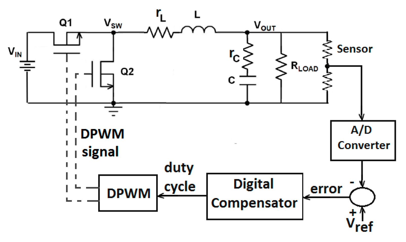
4. Synchronous Buck Converter Controller Design

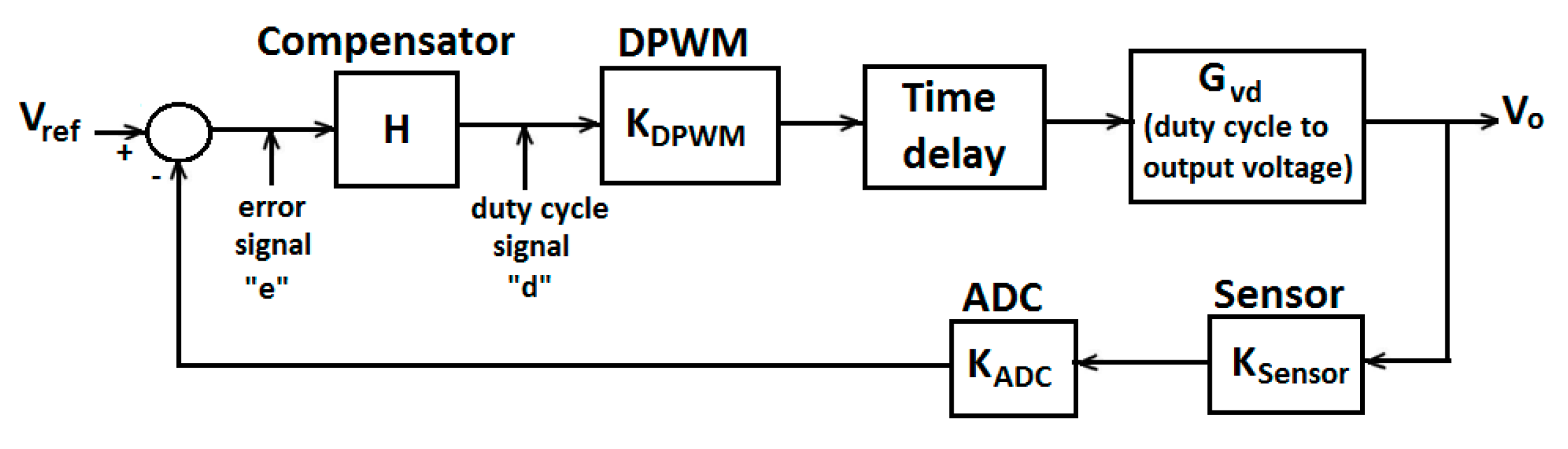
4.1. Closed-loop Control System

Figure 3 below shows a synchronous buck converter with its digital control feedback. It consists of four functional blocks: an ADC (analog-to-digital conversion), a compensator (error compensation), a DPWM (digital pulse-width modulation), and a synchronous buck converter power stage.
In this circuit, the goal is to minimize the difference between Vref and Vo. Therefore, authors need to design a digital PID compensator to track the error and bring it down to as small as possible.

4.2. Digital PID Compensator Design

For control purposes, the block diagram of the buck converter, which is used in this work, is shown in Figure 4.
The main blocks are the duty cycle-to-output transfer function of the power stage or plant (Gvd), the compensator (H), the total time delay of the control loop, the DPWM gain (Kdpwm), the ADC gain (Kadc) and the output voltage sensor gain (Ksensor).
For a buck converter, the small signal control to output transfer function is given by [10].
G v d ( s ) = V i ( s r c C + 1 ) s 2 L C ( R + r c R ) + s ( r c C ( R + r L R ) + L R + r L C ) + ( R + r L R )
The design parameters considered are shown in Table 1.
With the above design parameters, G v d ( s ) is given by:
G v d ( s )         = 1.48 e 07 s + 12 1.131 e 11 s 2 + 2.325 e 06 s + 1.005
The plant transfer function, including the effects of the ADC, DPWM and sensor is given by:
G v d s y s ( s ) = K s e n s o r K A D C K D P W M G v d e s ( t a d c + d T s + t d p w m )
where tadc is the ADC conversion time and tdpwm is the DPWM delay time.
In Equation (34), the exponent term represents the total time delay, which is usually taken equal to the switching period. That is, T s = ( t a d c + d T s + t d p w m ) . Then, the plant transfer function is given by:
G v d s y s ( s ) = K s e n s o r K A D C K D P W M G v d e s T s
The above transfer function presented in Equation (35) is used in the MATLAB control system toolbox to design the compensator in the analog domain. The designed compensator has a gain margin of 12.9 dB and a phase margin of 66.7 degrees. Note that, the phase margin is intentionally made higher to compensate for phase margin loss when converting to the digital form. The compensator so designed is then converted to its equivalent digital form using the bilinear transformation. The final digital PID compensator transfer function is given by:
G c ( z ) = 1.304 e 02 2.032 e 02 z 1 + 7.916 e 03 z 2 1 z 1

5. FPGA Implementation and Results Obtained

The digital PID compensator, an 8-bit sigma delta ADC and an 8-bit 1.5 MHz DPWM, as well as, all redundancy techniques have been implemented in MATLAB and Xilinx system generator. The overall objective is to properly regulate the output voltage towards the desired output voltage irrespective of the input voltage and any load variations within the given ranges and irrespective of radiation induced failure of any number of the duplicated modules based on the masking ability of the redundancy technique being used.

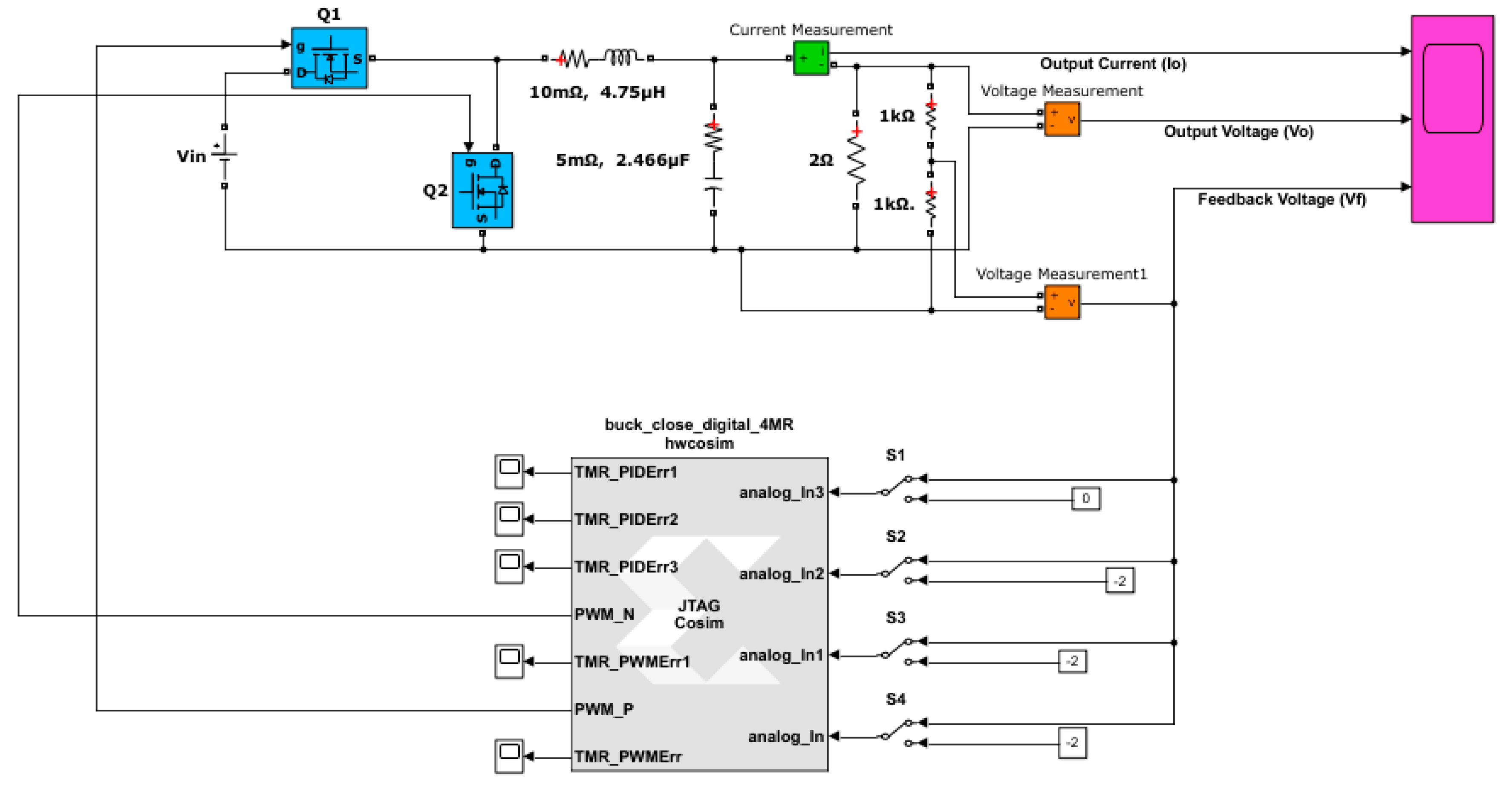
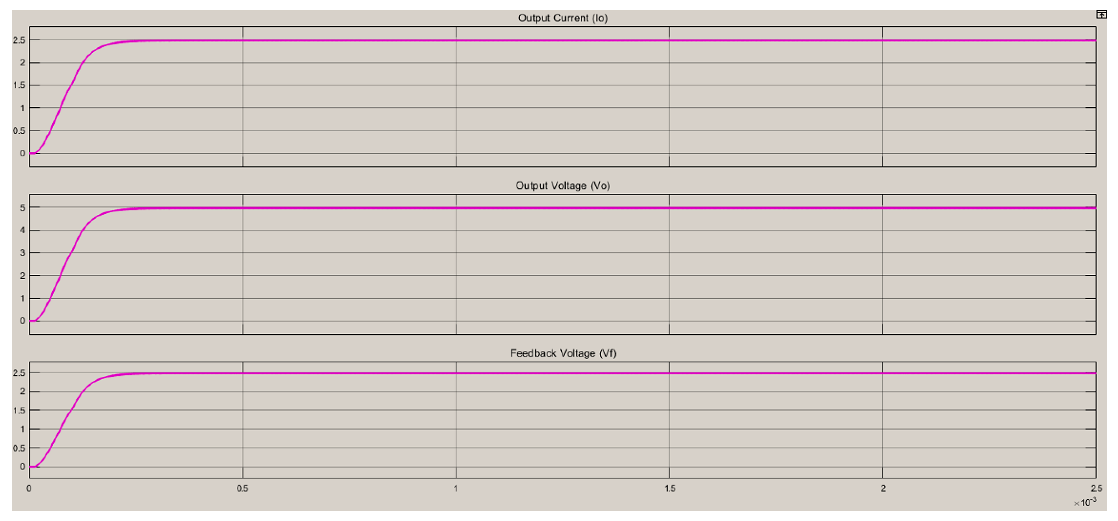
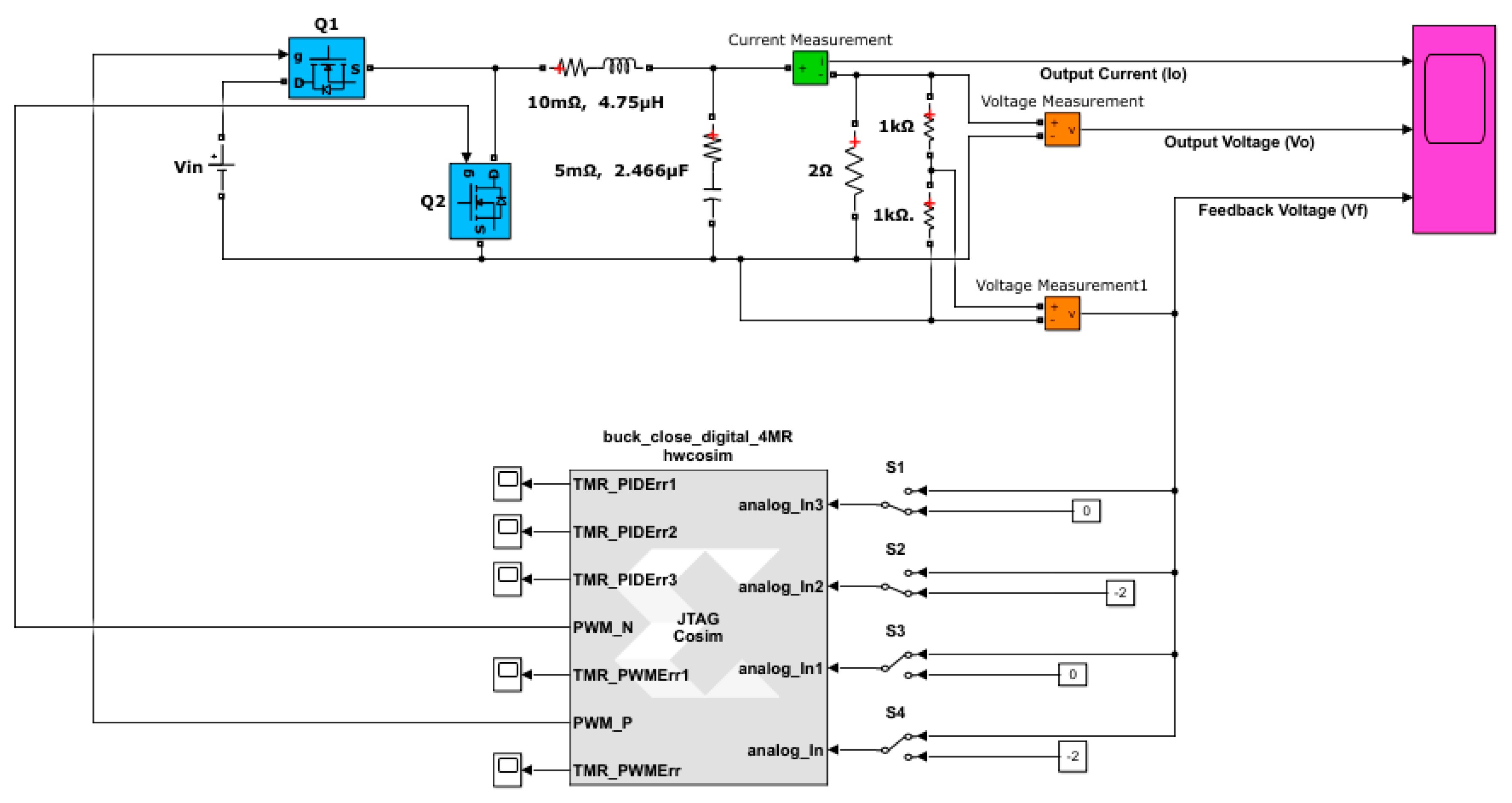
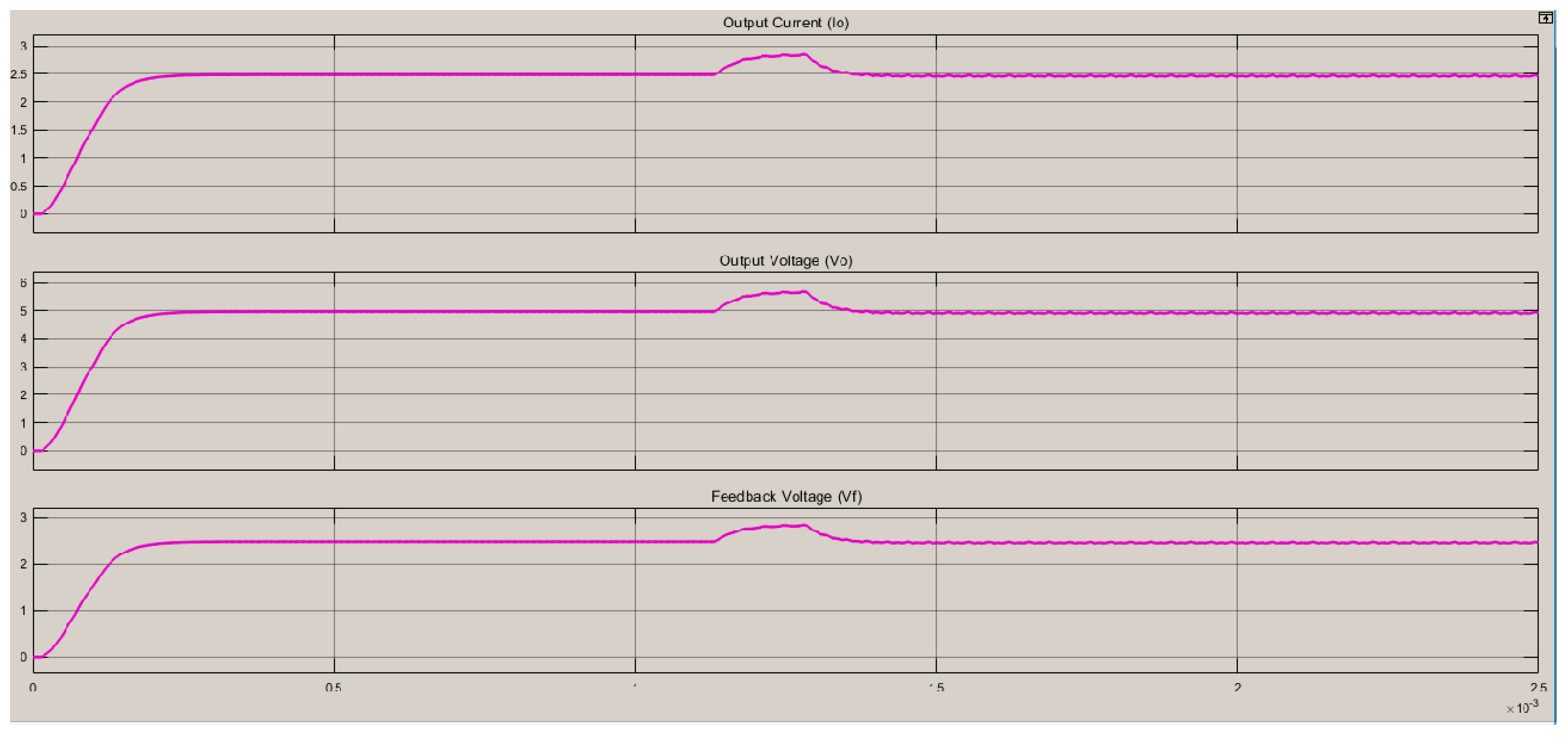
5.1. Hardware-in-the-Loop Simulation

It is practical to test the embedded controller more efficiently with a powerful method of hardware-in-the-loop (HIL) simulation. By thoroughly testing the controller in a virtual environment before proceeding to real-world tests of the complete system, one can maintain reliability and time requirements in a cost-effective manner. HIL simulation can also allow verifying whether the vendor specific FPGA synthesis tool actually retains the module level design, which is often not the case. Therefore, the HIL block is generated representing the radiation tolerant digital voltage mode controller for the synchronous buck converter.
The manual switches (S1, S2, S3, and S4), shown at the input of the controller HIL block diagram in Figure 5 are used to emulate the radiation faults during simulation; this is accomplished by switching the controller inputs to signals other than expected signals from the feedback system, or switching the inputs to ground (or, switch to zero). The duplicated voter’s, Ref [11] error detectors (PIDErr1, PIDErr2, and PIDErr3) and the DPWM signals voter’s error detectors (PWMErr1 and PWMErr2), shown at the output of the controller HIL block diagram in the Figure 5 can be used for repair/reconfiguration process initiation [12,13,14], when radiation faults occur in the respective voters, if such systems are used.
Figure 6 provides the converter output voltage and current without applying radiation fault emulation.
Figure 7 shows the HIL simulation block during fault emulation of modules 1 and 2.
Figure 8 presents the output voltage and current of converter under fault emulation of modules 1 and 2. Module 1 is switched to different signal at 0.5 m-second and then module 2 is switched to a different signal at 1 m-second to emulate the radiation fault. As it is clear from the Figure 8, there is a rise in voltage output of converter for short interval when switching the second module. This is due to switching transients.
There are five other different fault emulation cases available. All the other possible fault emulation combinations provided the same output voltages and currents as the case portrayed in the Figure 8.

5.2. Comparison of FPGA Resource Utilization and Reliability

As can be seen from Table 2, the proposed four modules redundancy uses the lowest hardware resources compared to FMR and the modified triplex–duplex redundancies while having the highest reliability compared to TMR and FMR techniques as explained earlier.

6. Conclusions

This paper presents a module level design approach to an FPGA based radiation tolerant digital voltage mode controller for a synchronous buck converter. A four-module high-reliability redundancy technique is proposed and implemented on zynq-7000 development board (Zybo). The technique has been compared with three other more common utilized redundancy techniques for reliability and FPGA resource utilization. It is observed that, the developed method has25% and 30% longer expected life than TMR and FMR techniques, respectively and requires lower FPGA resources compared to FMR and the modified triplex–duplex techniques.
It is shown that the proposed method can be used for radiation tolerant synchronous buck converter design for applications requiring relatively longer mission time, compared to TMR and FMR techniques. The work can be utilized in such applications where fault-masking ability of a system is required. For example space applications, power electronic converters applications, computers, satellites, high-energy physics experiments, etc.

Author Contributions

Conceptualization, S.B.; methodology, S.B.; software, S.B.; validation, S.B., B.K. and P.L.; formal analysis, S.B.; investigation, S.B.; resources, P.L.; writing–original draft preparation, S.B.; writing–review and editing, S.B. and P.L.; visualization, S.B.; supervision, P.L., V.D.S. and B.K.; project administration, P.L. and S.B.

Funding

This research was supported by the Home Grown PhD Program (HGPP) funded by the Ethiopian ministry of Education.

Conflicts of Interest

The authors declare no conflict of interest.

References

  1. Maurer, R.H.; Freeman, M.E.; Martin, M.N.; Roth, D.R. Harsh Environments: Space Radiation Environment, Effects, and Mitigation; John Hopkins University: Baltimore, MD, USA, 2008. [Google Scholar]
  2. Leonard, C. Challenges for Electronic Circuits in Space Applications. Analog Devices, Inc. Available online: https://www.analog.com/media/en/technical-documentation/tech-articles/Challenges-for-Electronic-Circuits-in-Space-Applications.pdf (accessed on 1 July 2018).
  3. Jagannathan, S.; Herbison, D.R.; Holman, W.T.; Massengill, L.W. Behavioral Modeling Technique for TID Degradation of Complex Analog Circuits. IEEE Trans. Nucl. Sci. 2010, 57, 3708–3715. [Google Scholar] [CrossRef]
  4. Schmidt, F.H., Jr. Fault Tolerant Design Implementation on Radiation Hardened by Design SRAM-Based FPGAs. Master’s Thesis, Massachusetts Institute of Technology, Boston, MA, USA, 2013. [Google Scholar]
  5. Jain, M.; Gupta, R. Redundancy Issues in Software and Hardware Systems—An Overview. Int. J. Reliab. Qual. Saf. Eng. 2011, 18, 61–98. [Google Scholar] [CrossRef]
  6. Kolte, P.P.; Maheshwari, R.; Ajankar, S. Triple modular redundacny using fault tolerant technique—A review. In Proceedings of the International Conference on Emanations in Modern Technology and Engineering ICEMTE-2017, Maharashtra, India, 4–5 March 2017; Volume 5. [Google Scholar]
  7. Istiyanto, J.E.; Harjoko, A.; Putra, A.E. Five modular redundancy with mitigation technique to recover the error module. Int. J. Adv. Stud. Comput. Sci. Eng. 2014, 3, 1–6. [Google Scholar]
  8. Quintana, J.M.; Avedillo, J.M.; Huertas, J.L. Efficient Realization of a Threshhold voter for Self-purging Redundancy. J. Electron. Test. 2001, 17, 69–73. [Google Scholar] [CrossRef]
  9. Losq, J. A highly Efficient Redundancy Scheme: Self-purging Redundancy. IEEE Trans. Comput. 1976, C-25, 569–578. [Google Scholar] [CrossRef]
  10. Choudhury, S. Designing the Digital Compensator for a UCD91XX-Based Digital Power Supply; Texas Instruments Application Notes; Texas Instruments: Dallas, TX, USA, 2007. [Google Scholar]
  11. Carcheri, J.C. N-Modular Redundancy Techniques for Fault Tolerance in Reconfigurable Logic Devices; Master’s Project Report; UCF: Orlando, FL, USA, 2007. [Google Scholar]
  12. Uznanski, S.; Brugger, M.; Schramm, V.; Thurel, Y.; Todd, B. Radiation Tolerant Power Converter Design for the LHC; CERN CH-1211: Genève, Switzerland, 2012. [Google Scholar]
  13. Van Vonno, N.W.; Pearce, L.G. Total dose and single event effect testing of hardened point of load regulator. In Proceedings of the Radiation Effects Workshop (REDW), Denver, CO, USA, 20–23 July 2010; pp. 80–88. [Google Scholar]
  14. Wang, J.J. Radiation Effects in FPGAs; Actel Corporation: Mountain View, CA, USA, 2008. [Google Scholar]
Figure 1. Modified triplex–duplex Redundancy.
Electronics 08 00513 g001
Figure 2. Proposed four modules redundancy.
Electronics 08 00513 g002
Figure 3. A synchronous buck converters with closed-loop digital control.
Electronics 08 00513 g003
Figure 4. Buck converter control system point view.
Electronics 08 00513 g004
Figure 5. Hardware-in-the-loop (HIL) simulation block including the power stage.
Electronics 08 00513 g005
Figure 6. Converter output voltage and current during HIL simulation for the case Vi = 16 V and Rload = 2 Ω without fault emulation.
Electronics 08 00513 g006
Figure 7. HIL simulation block including the power stage during fault emulation of modules 1 and 2.
Electronics 08 00513 g007
Figure 8. Converter output voltage and current during HIL simulation for the case Vi = 16 V and Rload = 2 Ω with fault emulation of modules 1 and 2.
Electronics 08 00513 g008
Table 1. Design parameters of the converter.
ParameterRating Value
Input Voltage (Vi)12 V, (11–16 V)
Output Voltage (Vo)5 V
Output Current (Io)2.5 A, (1.25–5 A)
Inductor (L), ESR4.75 µH, 10 mΩ
Capacitor (C), ESR2.466 µF, 5 mΩ
Load (R)2 Ω, (1–4 Ω)
Switching Frequency (Fsw)1.5 MHz
Table 2. FPGA resource utilization summary and reliability comparison.
MethodsDSPsLUTsRegisters Reliability   ( λ   =   10 % )
Mission Time t
AvailableUsedPercentageAvailableUsedPercentageAvailableUsedPercentaget = 1 yeart = 5 Years
Simplex8011.2517,6006473.6835,2003010.860.90.6
TMR33.75193410.998742.480.97460.6574
Proposed Four Module Method45271015.411893.380.99680.8282
FMR56.25319518.1514464.110.99260.6938
Modified Triplex–duplex67.5405323.0317294.911.00.9620

