Single Event Transients in CMOS Ring Oscillators

Department of Electrical Engineering (ESAT), KU Leuven, 3000 Leuven, Belgium
*
Author to whom correspondence should be addressed.
Electronics 2019, 8(6), 618; https://doi.org/10.3390/electronics8060618
Submission received: 28 April 2019
/
Revised: 24 May 2019
/
Accepted: 29 May 2019
/
Published: 1 June 2019
(This article belongs to the Special Issue Radiation Tolerant Electronics)
Abstract
:In this paper, a time-variant analysis is made on Single-Event Transients (SETs) in integrated CMOS ring oscillators. The Impulse Sensitive Function (ISF) of the oscillator is used to analyze the impact of the relative moment when a particle hits the circuit. The analysis is based on simulations and verified experimentally with a Two-Photon Absorption (TPA) laser setup. The experiments are done using a 65 nm CMOS test chip.
1. Introduction
Integrated, high-speed clock generation circuits are essential blocks in nearly all modern silicon systems. A wide variety of circuits and architectures is available in the literature. Most design choices depend on the desired quality and frequency of the generated clock signal and the reference clock. The vast majority of high-speed clock generators employ a Phase Locked Loop (PLL) [1] that ensures a fixed frequency multiplication and a known phase relationship between the on-chip high-speed oscillator and off-chip reference clock. However, other architectures such as Delay Locked Loops (DLLs) [2] and Multiplying DLLs (MDLLs) [3] are gaining more interest over the past years.
The quality of a synthesized clock mainly depends on the quality of the reference clock and the on-chip oscillator [4]. While the latter is in the hand of a designer, the former is usually not. Therefore, the study of integrated CMOS oscillators has been an interesting research topic for the past decades. Two main types of oscillators are commonly used: LC-tank oscillators and ring oscillators [5]. LC-oscillators rely on a resonant tank of an inductor and a capacitor which resonates at a frequency . They are known to exhibit superior phase noise and jitter performance and are widely used in low jitter clock synthesis, down to 100 fs RMS and low phase noise local oscillators for wireless communication links where out-of-band phase noise can limit the performance in the case of a strong interferer [6,7]. While the performance and power efficiency of an LC-oscillator is excellent, the main downside is its large area and limited tuning range. Typically, the inductor occupies more than 150 × 150 . Secondly, since the quality factor of the inductor peaks in the GHz frequency range but falls for lower frequencies, such oscillators are rarely used below several 100 MHz without the use of a divider. When such extremely low noise levels are not mandatory, integrated ring oscillators can prove their usage. In terms of area usage, ring oscillators can be as small as a few tens of digital gates [8]. They rely on the total delay of a closed loop of digital delay cells. Ring oscillators find their application on digital systems such as microprocessors, complex SoCs and serial communication links.
Today’s most advanced electronic systems also find their application in harsh environments containing ionizing radiation. Examples of applications are space systems such as satellites and deep space probes [9], high-energy physics experiments such as the ATLAS [10] and CMS detectors [11,12] at the Large Hadron Collider (LHC) at CERN. However, terrestrial applications such as autonomous airplanes, cars and high-reliable computing systems in data centers are also affected by ionizing radiation. Charged particles that impact a silicon chip can generate charges in the silicon. This occurs nearly instantly when a particle crosses the circuit. When this occurs near the active source and drain junctions of a transistor, these charges can be collected by the junctions and injected in the circuit. In digital circuits, these Single Event Effects (SEEs) are Single Event Transients (SETs) or Single-Event Upsets (SEUs). The former is only a temporal error while the latter remains erroneous. SEEs also strongly impact the oscillator in a clock generator. In particular, SEEs generate phase transients in the clock that can cause errors in synchronous logic clocked by the clock generator. Especially when timing is critical, phase jumps as large as 20 ps can be catastrophic for the reliability of a digital platform. Therefore, a solid understanding of the basic mechanisms of SEEs in CMOS ring oscillators is essential to give more insight in hardening and protection methods of these blocks.
This paper is organized as follows. Section 2 introduces a time-dependent model for the sensitivity of an oscillator to current impulses, which is applied to estimate its response to SEEs. In Section 3, experiments are shown that prove the time-dependent radiation effects using a two-photo laser absorption setup. Finally, conclusions are drawn.
2. Time Dependent Effects in Oscillators
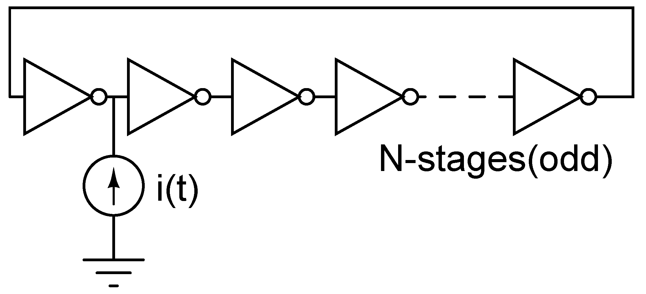
A commonly used theory to understand translation of white and colored noise sources in oscillator circuits is the Linear-Time-Variant (LTV) noise theory of Hajimiri [13,14,15]. In this theory, noise is modeled as a current source injecting pulses on the different nodes of the oscillator, as depicted in Figure 1. This image shows an abstract (high-level) representation of a ring oscillator where a current impulse is injected at one particular node, which is used in the analysis below. The shown oscillator has N odd amount of stages for the analysis. This current pulse is causing phase steps in the oscillator, which are integrated over time, resulting in an uncertainty on the phase, also called phase noise. The impact of the injected pulses is weighted by the so-called Impulse-Sensitivity-Function (ISF), a dimensionless and frequency-independent function determining the sensitivity of the oscillator node to the injected noise. The instantaneous value of the ISF is a direct measure for the noise-to-phase transfer function of the oscillator [16]:
where t is the time, is the moment of impact of the current pulse, is the current-to-phase impulse response, is the ISF at time , is the charge displacement during an oscillator cycle (proportional to the amplitude) and is the unit step function. Since the oscillator is assumed to be a LTV system, the superposition principle can be applied to calculate the impact of a infinite series of pulses:
where represents the integrated phase deviation compared to the ideal oscillator and is the injected noise current over time. In [13], it is shown that application of the LTV approach to a noise spectrum results in the typical noise shape around the oscillator carrier. In this article, the ISF is used to calculate the impact of current pulses caused by a particle strike on a four-stage ring oscillator.
In Figure 2, a waveform is shown where a disturbance is injected at two different moments in time. In Figure 2a, a current impulse is injected in the maximal saturated region of the oscillator. Since the current does not change in the saturated shape of the waveform, the ISF for current injections in this region is approximately zero. However, as shown in Figure 2b, when the current is injected during the signal transition times, the total phase error is maximal. In general, the ISF is proportional to the slew rate of the waveform, which is large during transition.
2.1. Calculation of the ISF
To calculate the ISF of an oscillator, different methods are described in the literature [13]. The first method is based on circuit simulations where a current pulse is injected at different moments spread along the oscillator period. By calculating the induced phase shift, the ISF can easily be calculated. However, more analytical methods are also available, making use of the state space description of an oscillator. In a ring oscillator, the state variables can be considered to be the node voltages at the output of each stage. After all, a state variable is an independent memory state in the system: a current through an inductor or a voltage across a (parasitic) capacitance [15]. In this case, the ISF for a pulse injected at the output node of stage i of an n-stage oscillator can be written as:
This shows that the ISF is low (zero) when the node voltage is constant and high during the transients. In [16], the ISF of a ring oscillator is approximated by a flat line equal to zero, with a triangular (alternating positive and negative) pulse at each transient of the considered oscillator node. Although this is a piecewise linearized approximation, the results for a typical statistical noise source are satisfying.
The approximation, however, only holds for oscillators of which the node voltages are strongly saturating against the supply rails with sharp transients in between. The oscillator considered in this article is based on a differential Maneatis cell, resulting a much smoother and non-saturating waveforms and therefore also a smoother shape of the ISF.
2.2. Particle Strikes as a Noise Source
Similar to noise, charged particles ionize the silicon substrate resulting in free charges in the substrate. In the region of the source and drain junctions of the transistors, these charges can be collected in the junctions by the strong electric field in the depletion region. As such, a part of the generated charges is injected in the circuit nodes. An exact calculation of the impact is a tedious and complex task: analytical methods are based on approximations and are therefore often inaccurate; numerical TCAD simulations, on the other hand, are considered to present the most accurate results but are time-consuming and sensitive to doping and geometry inaccuracies. The most common issue here is that many of the technology parameters are unknown to designers. A well accepted model to assess charge injection in analog circuits is the double exponential current shape [17]:
where Q is the total collected charge and a and b are technology dependent time constants. In the case where the time constants are significantly faster than the overall circuit dynamics, the injected current can be simplified as an impulse current:
For a particle strike at time , the resulting phase error is equal to (using Equation (1)):
The previous analysis only considered a single node in the oscillator. Practically, an oscillator is built with N stages where N is odd for single ended oscillators and N can be either even or odd for differential oscillators. An oscillator will oscillate at a frequency:
in which is the gate delay per stage and N is the number of stages. The signal waveform is therefore shifted between two successive stages by . As a consequence, the ISF is also shifted between successive stages. The current-to-phase impulse response for all successive stages in an inverting ring oscillator is therefore:
where i = [0…(N − 1)] represents each stage. This is elaborately discussed in [14]. The time-shifting is experimentally shown in Section 3 by measuring the ISF at different stages in the experimental design. The phase shift of all stages is considered to be of significant interest for phase noise analysis and noise folding due to common noise sources, such as supply or substrate noise. However, since radiation effects are only impacting one node simultaneously (if the cells are sufficiently large), each stage can be represented by the same ISF and the phase shift can be ignored.
3. Experiments
3.1. Experimental Circuit Description
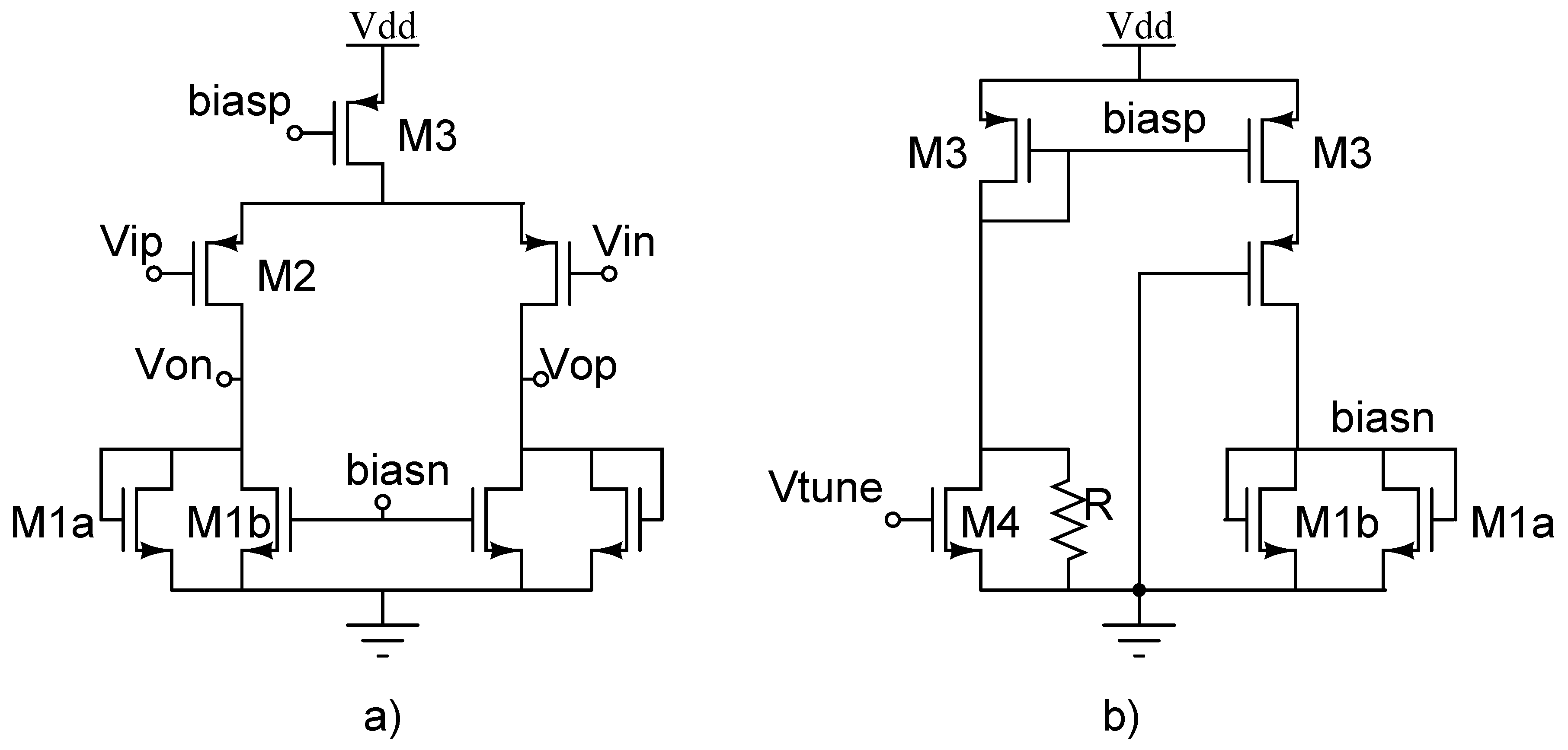
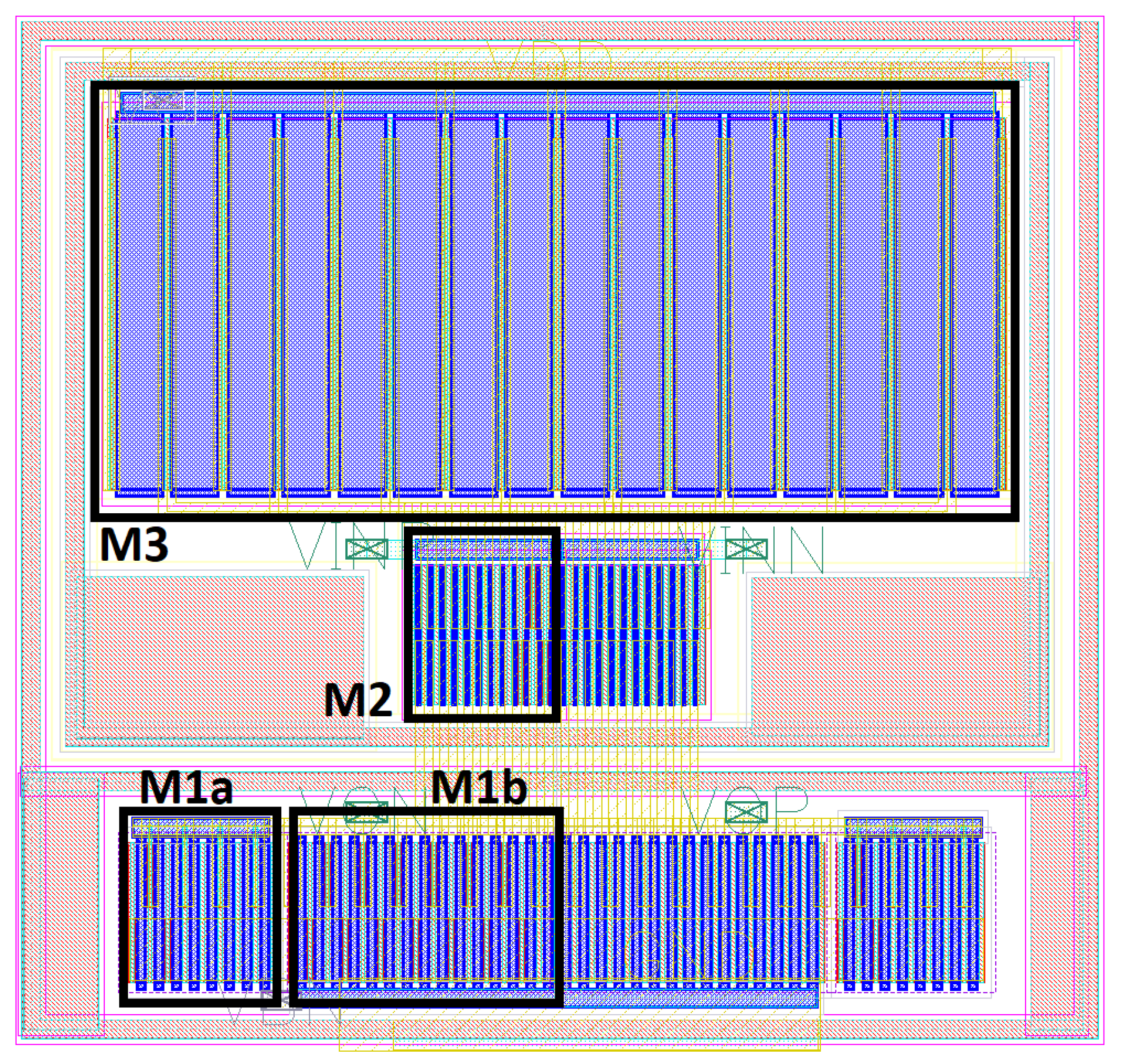
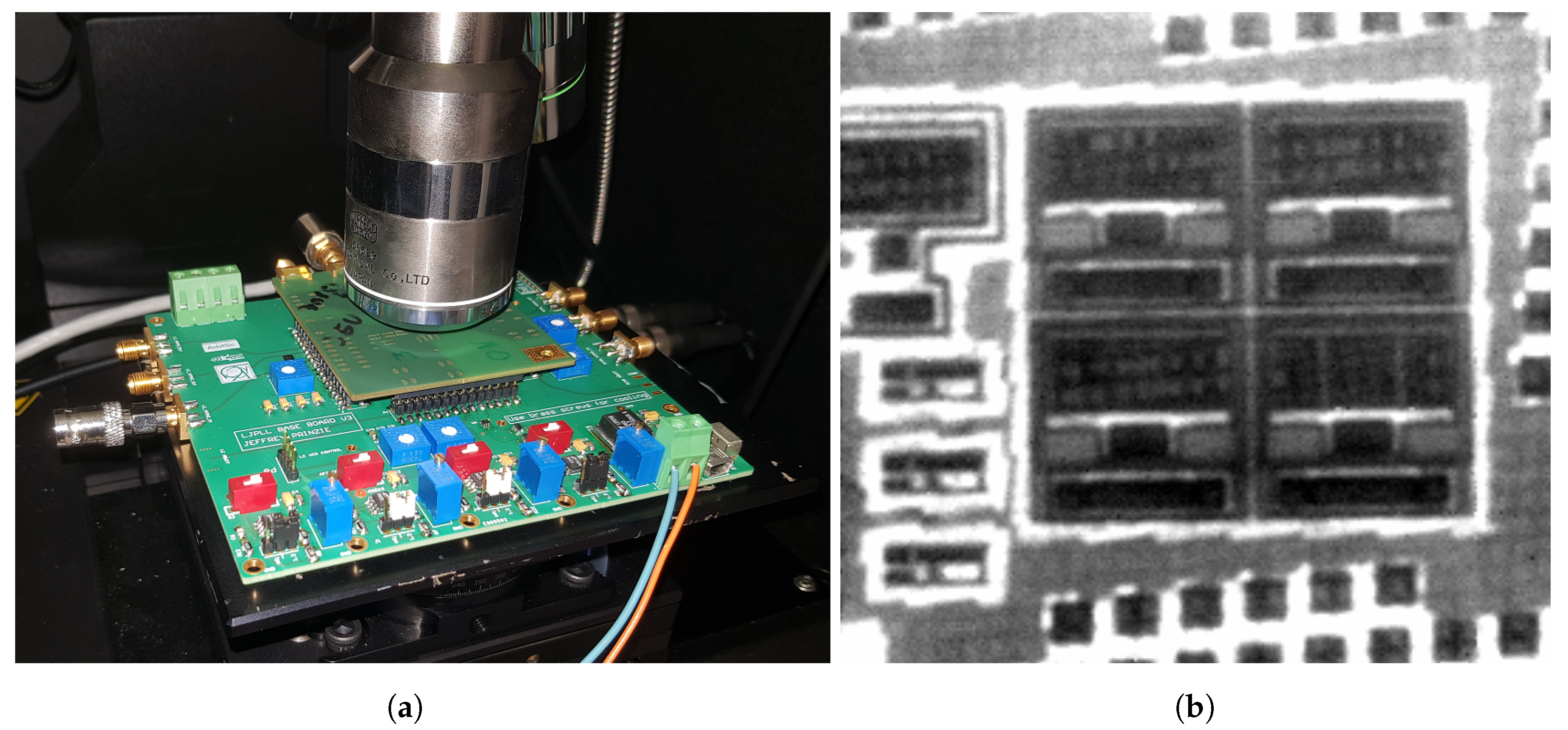
To quantify the magnitude of the ISF experimentally, a ring oscillator was designed and prototyped in a 65 nm CMOS technology with standard-Vt devices an a core voltage of 1.2 V. The oscillator had four differential voltage controlled delay stages and oscillates from 1.5 GHz to 3.2 GHz with a nominal frequency of 2 GHz (further assumed in all experiments). The circuit schematic of the delay cells is shown in Figure 3a and was designed for these experiments based on a well known and frequently used Maneatis delay cell [18]. A PMOS equivalent circuit of the Maneatis delay cell was designed to reduce 1/f noise. In addition, the bias block from [18] was used. The transistor sizes were chosen to meet the target frequency of 2 GHz in this technology. The delay through the ring was adjusted using the bias voltage of M3 (biasp), which regulated the current through the cells. The bias voltage of the NMOS load was adjusted to keep the oscillation amplitude relatively constant. These voltages were generated by a bias generator, as shown in Figure 3b, which was shared by all stages. M4 converted the VCO input tuning voltage to a current that was mirrored by M3. The right branch was a replica of the delay cell, which stabilized the oscillation amplitude. A bypass resistor ensured that a non-zero current flowed when the tuning voltage was equal to zero (or below of M4) to prevent a failure in oscillation. The layout of a single delay cell is shown in Figure 4. PMOS and NMOS devices were isolated with two p- and n-guard rings to reduce the probability of latch-up. Devices M1a and M1b had identical finger widths and shared the same drain and source voltages. Therefore, when considering the charge collection after a particle strike, the drain nodes of M1a and M1b behaved in exactly the same fashion. The full layout of the ring oscillator is shown in Figure 5. The left part of the layout consisted of the bias circuitry. The right part was the four-stage differential ring oscillator. The red dots indicate the locations where the laser was focused and charges were injected during the experiments. In each stage, both M2 and M1a were studied. For the reason explained above, M1b is not reported since its results were identical. Further circuit details on the design and electrical measurements of the ring-oscillator are reported in [19].
3.2. Simulation Results
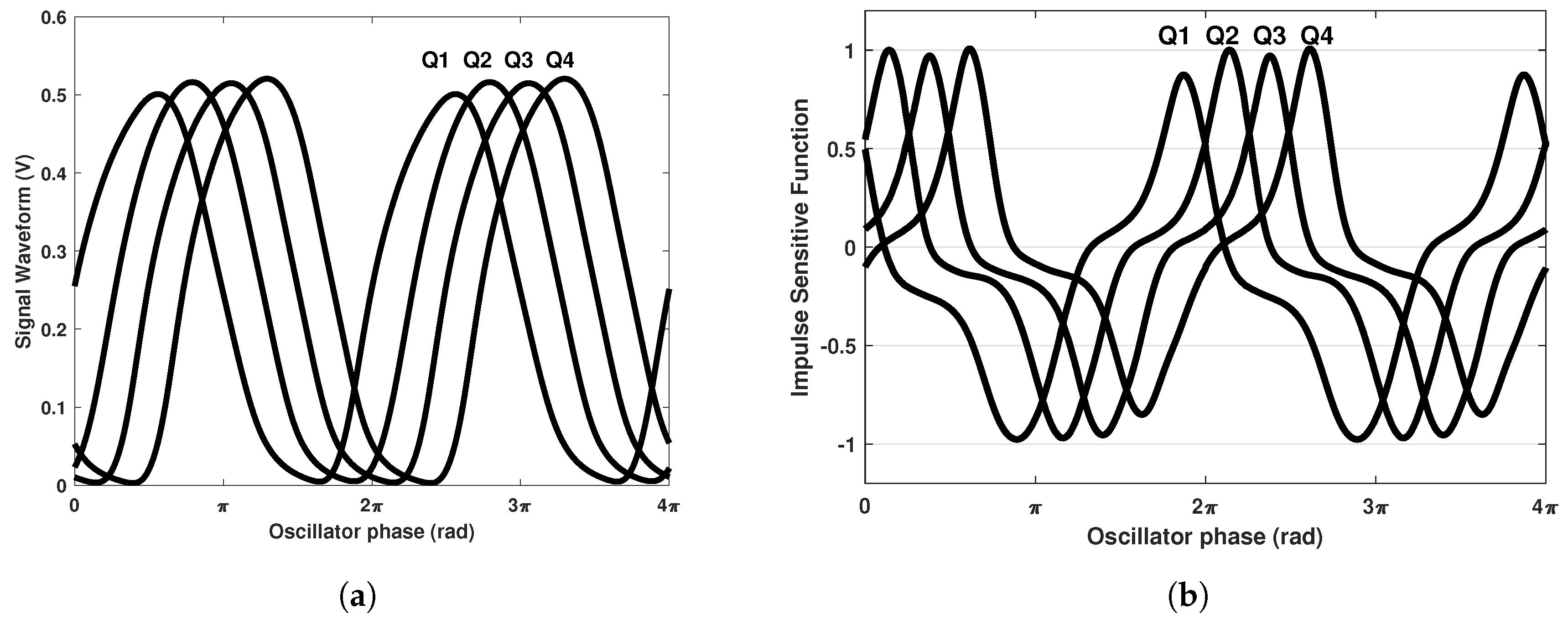
To qualify the measurements, a simulation was performed to correlate with the simulated data. The ring oscillator was simulated using a periodic steady state (PSS) analysis, using a shooting engine. The PSS resolved a periodic behavior of the circuit and determined the harmonic content of the waveform [20]. This technique was commonly used to analyze the performance of an oscillator. The signal waveforms at the internal nodes of the oscillator are shown in Figure 6a, respectively, Q1–Q4 of on each delay stage. The phase of the four waveforms was distributed in the interval 0-. This was slightly different from what is traditionally expected from a ring oscillator. However, since the number of stages was even, an inversion was made by crossing two oscillator waveforms in the loop. Otherwise, the oscillator would fail to oscillate. As a consequence, at the oscillation frequency, the total phase delay of all stages should only satisfy . The same phase distribution was visible in the results and measurements of the ISF.
The simulation of the ISF was done using the pulse projection vector (PPV) method, available in PSS simulators [21,22]. This method estimated the amount of phase deviation that originated from a disturbance at a particular node, which represented the ISF of the oscillation node. An alternative method would be to run several transient simulations and measuring the phase error, resulting from narrow current pulses, injected at various successive moments in time. While the latter was similar to the experimental setup, it required relatively large post processing and less accuracy than the former method. The results of the simulations of the ISF are shown in Figure 6b. As expected, the ISF of each successive stage was shifted with respect to the preceding stage, similar to the phase deviation in the signal waveform. As discussed above, the oscillator was mostly sensitive to current impulses, which were injected near the steep edges of the waveform.
3.3. Experimental Measurement Setup
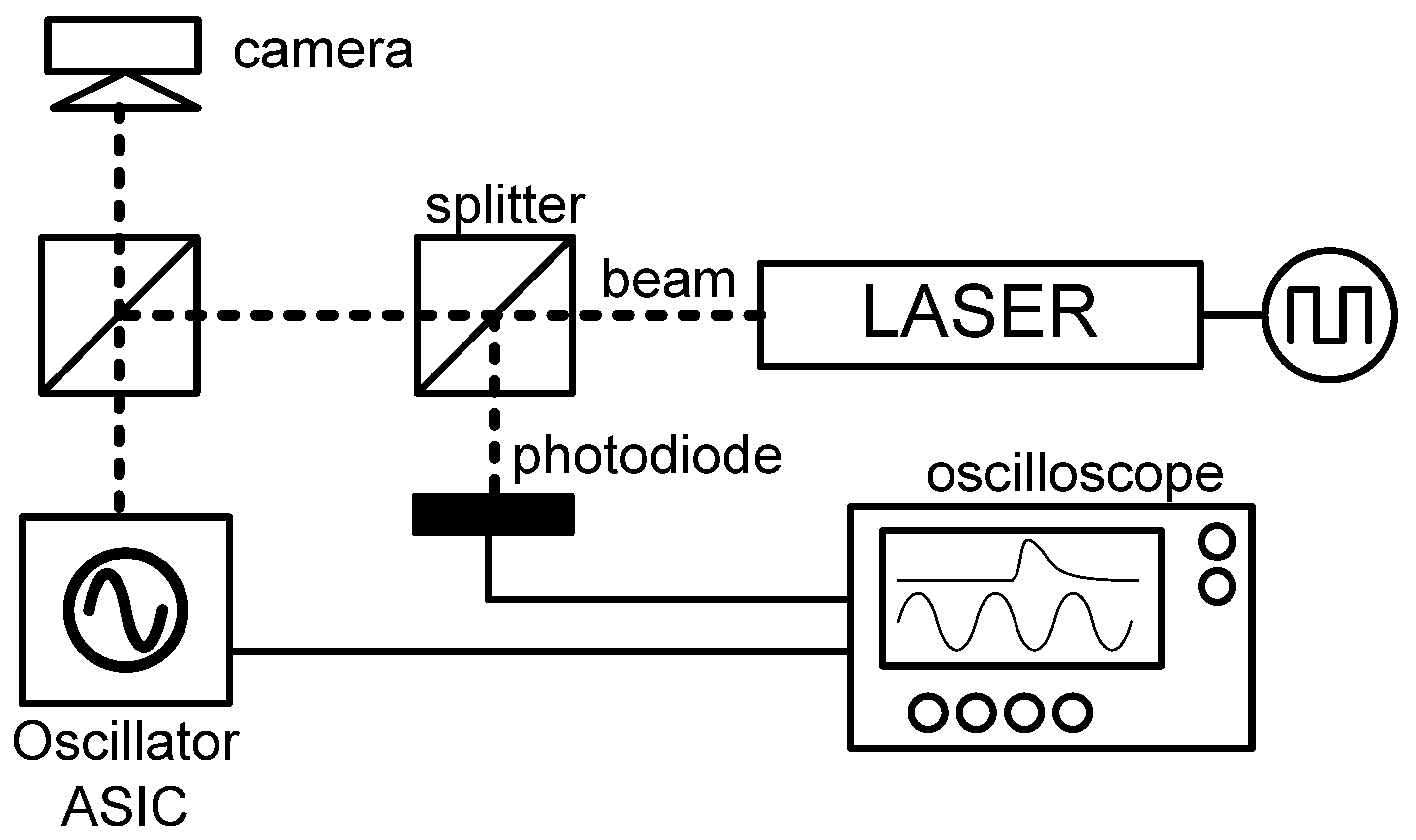
To experimentally prove the time dependency of the phase errors to the moment when the charge was collected, a setup was used with a two photon absorption (TPA) laser. An abstract representation of the setup is shown in Figure 7. A femto-second laser pulse was generated at a pulse rate of 100 Hz, which was generated in the laser source and was not synchronized to the electrical setup. The laser beam was focused on the chip and locally generated free carriers near the focal point of the beam by means of the non-linear two photon absorption mechanism. This allowed accurately generating charges only locally in the silicon substrate with spot sizes of < 1 m. To measure the ISF of the oscillator, either the laser clock needed to be synchronized to the oscillator or the arrival time of the laser pulse needed to be measured. Practically, the latter was preferred since the laser arrival time could be accurately measured by extracting part of the laser beam and detecting it with a photo detector, which converted the laser pulse to an electrical signal. The accuracy of the arrival time detection was limited by the intrinsic noise of the detector but a jitter of less than 2 ps could be achieved. The setup was based on a statistically random sampling of different arrival times of the laser beam on the chip. Since the laser clock was asynchronous to the oscillator, the pulse could arrive at any moment in time. Both the oscillator waveform and the photo diode signal were captured by a high speed sampling oscilloscope. The scope was triggered by the laser clock, which indicated an occurrence of a pulse. The relative phase of the pulse to the oscillator phase was extracted by post-processing by measuring the time difference between the photo detector signal pulse and the oscillator edge. This calculation provided the injection time, relative to the oscillator zero-crossing, as well as the X-data point of the sampled ISF. The vertical value of the ISF was the total phase error that was caused by the laser pulse. This was also measured by comparing the phase of the oscillator before and after pulse injection. A picture of the experimental setup is shown in Figure 8. Figure 8a shows the test board of the chip with the focusing lens of the laser. The laser beam was injected vertically and focused on the substrate of the chip. As shown in Figure 7, a second bidirectional splitter was used to visualize the substrate of the chip with an infrared camera. A snapshot of the layout that was investigated is shown in Figure 8b.
3.4. Experimental Results
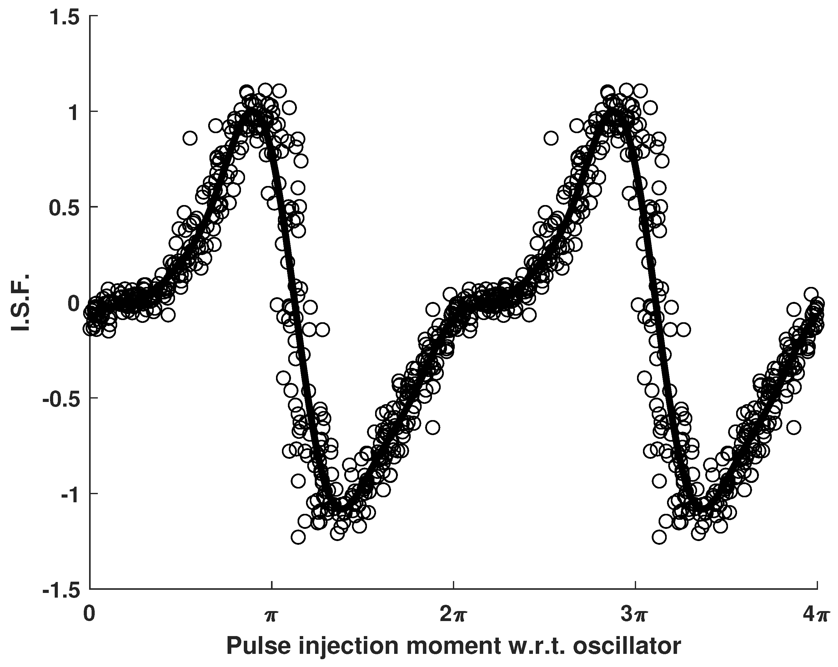
The results of an injection campaign on the NMOS device M1a of the first stage is shown in Figure 9. The X-axis shows the moment when the pulse was injected, relative to the oscillator zero-crossing. The Y-axis shows the phase error caused by the pulse. Each pulse provided a single point in the scatter plot. Although the waveform of the ISF was periodic in 2, two periods are shown in Figure 9 to improve readability. However, the data in the interval 2–4 were identical to the first period. In total, 500 pulses were injected in the oscillator. The measurement time was not limited by the laser pulse frequency but by the processing time of the sampling oscilloscope to save the data upon trigger. The scatter plot was used to fit a periodic function with eight harmonics and qA overlaid to the data points. The measurements clearly indicated that the phase error was highly time-dependent as estimated beforehand. The fit of the scatter plot achieved an R = 0.88, which was of sufficient quality to analyze and compare the ISF from the fitted curves. This could also be observed well from the plot.
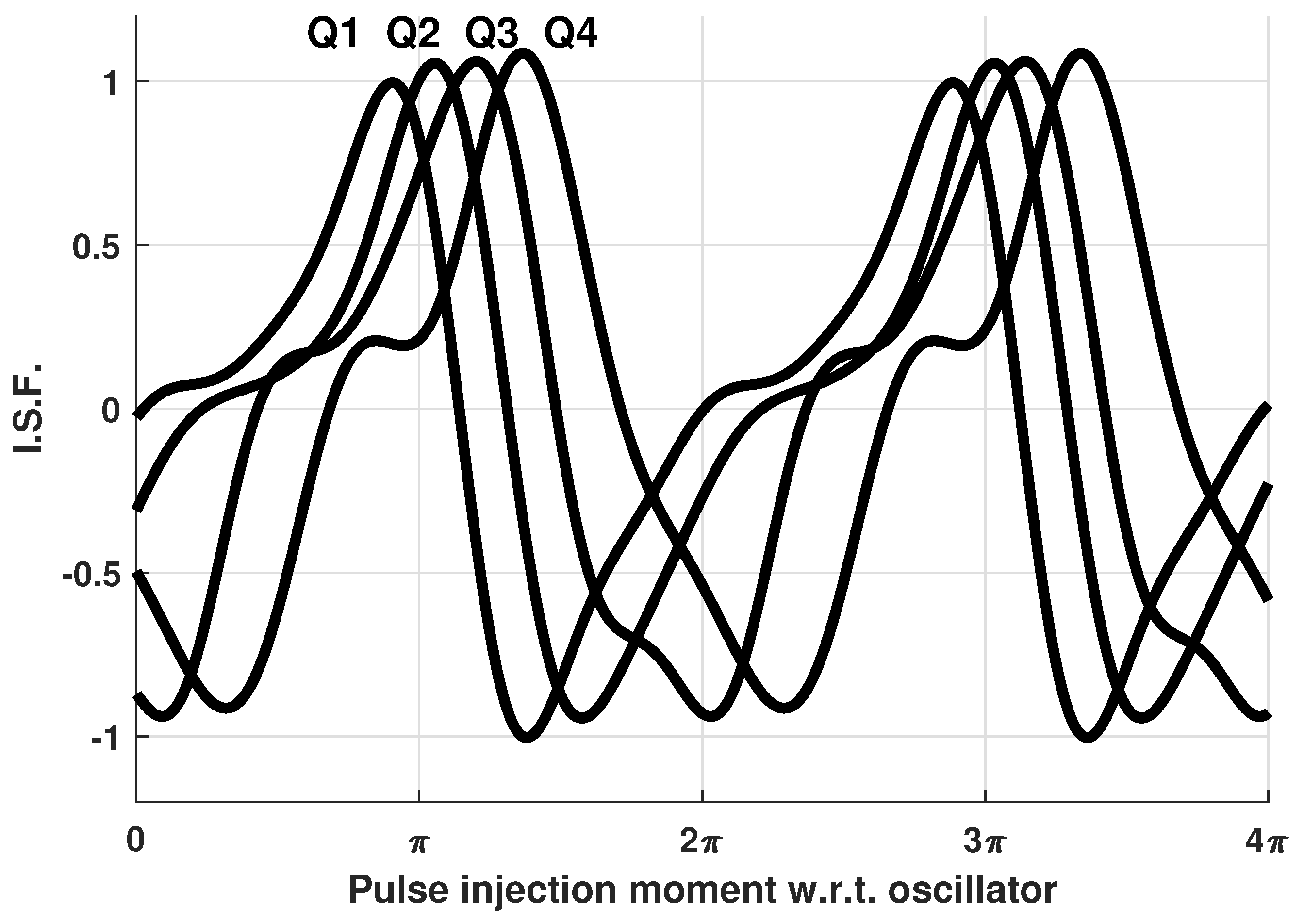
To further analyze the periodic behavior of the oscillator for injected charges, the same analysis was made on all four stages of the oscillator. Although the absolute arrival time of the laser with respect to the oscillator could not be measured, a relative comparison could be made. This occurred since several delays in the setup were not accurately known. Firstly, the relative delay in the laser beam between the pulse arriving at the photo diode and the one actually arriving at the chip was not known. Secondly, several coaxial SMA cables were used to measure the signals on the oscilloscope. Both delays, however, were static and identical for all measurements and were considered as a bias for our setup. The results of injections at all four stages (M1a) is shown in Figure 10. Each ISF was measured by the method described sbove. For improved readability, only the fitted curves are shown here, representing the ISF of the oscillator node. As expected and similar to the simulations, the ISF of the successive stages was phase shifted due to the delays of the oscillator at its oscillation frequency. From these measurements, it became clear the the presented theory could be accurately applied to investigate the impact of SEEs to ring oscillators. A careful observation of the four ISF waveforms indicated that the shapes of the four successive stages were not identical. This was due to a change in the laser focus, which was difficult to control accurately across a wide area, such as this device. If the device was not planar or was slightly tilted, the vertical focus of the laser changes with position and the charges were generated at different depths, resulting in deformed effects. However, a manual refocus was done for each measurement to match the collected charges at all nodes as accurately as practically achievable.
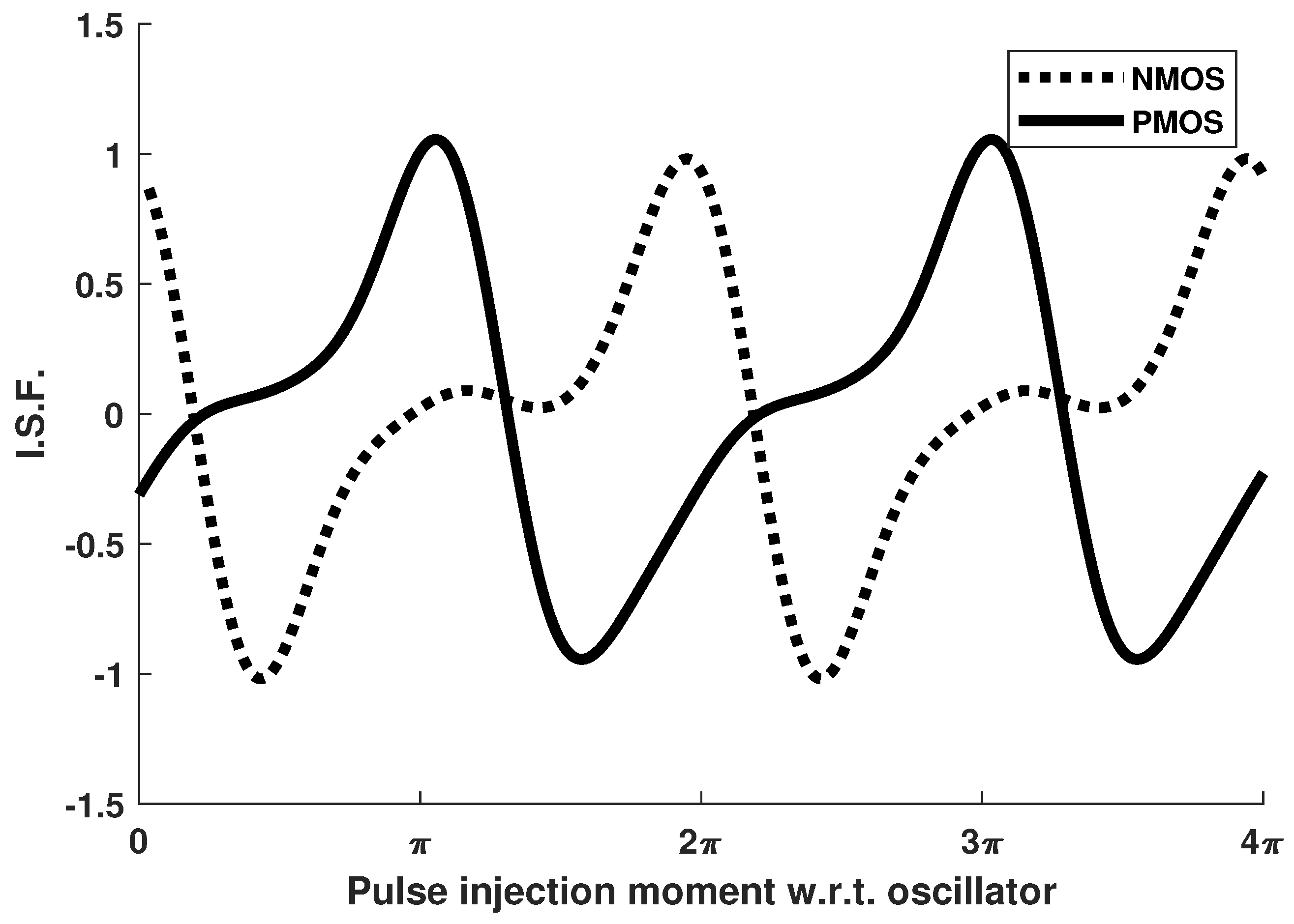
Both experiments shown above only present results from charges that were collected by the NMOS devices, the junctions of which could only drain charge from the oscillator nodes to the substrate. However, if charges were collected by the PMOS device M2, these junctions could only supply charges from the supply (nwell) to the output node. Therefore, the charge injection of PMOS and NMOS was opposite and the measured phase shift was inverted as well. Figure 11 shows both ISF waveforms of the first stage when the laser was focused on both the PMOS and NMOS device in the oscillator. These results clearly indicate the inversion of the phase error due to a reversed current flow.
One node which was not addressed in the results was the drain of M3. This is a common-mode net in the delay cells. Therefore, it is expected that this node does not contribute to a direct phase error since the effects on both differential nodes cancel. However, one could expect a frequency error since the common mode voltage could impact the delay of the stage. However, this effect was experimentally negligible and is therefore not discussed.
4. Conclusions
This paper presents a time-dependent analysis on Single-Event Transients on CMOS ring oscillators. The analysis is based on the periodic Impulse Sensitive Function (ISF) of an oscillator, which represents the phase error due to an impulse current that predicts that Single-Event Transients are time-dependent. It was shown that the oscillator phase error due to radiation depends on the moment when charges are injected to the circuit, relative to the phase of the oscillator. To prove the theoretical analysis, a test chip was manufactured in a 65 nm CMOS technology to measure the time-dependent effects. A measurement campaign is presented that, for the first time, proved this theory experimentally in the time-domain and verified the proposed analysis in practice. The experiments were done with a Two-Photon Laser setup to inject charges in the silicon devices with a measurement accuracy better than 2 ps. The measurements were done based on statistical random sampling of the pulse arrival time with respect to the oscillator waveform. The measurements showed that the ring oscillator’s phase error depends on the moment when charges are generated in the devices, which correlate with the signal waveform. It was also observed that the ISF of different stages is phase shifted, which was predicted by the theoretical analysis. We can therefore conclude that the theoretical models can be applied to calculate Single-Event Transients in CMOS ring oscillators. where possible.
Author Contributions
Conceptualization, J.P. and V.D.S.; methodology, J.P. and V.D.S.; validation, J.P. and V.D.S.; investigation, J.P. and V.D.S.; and writing—original draft preparation, J.P. and V.D.S.
Funding
This research was funded by FWO.
Conflicts of Interest
The authors declare no conflict of interest. The founding sponsors had no role in the design of the study; in the collection, analyses, or interpretation of data; in the writing of the manuscript, and in the decision to publish the results.
References
- Young, I.A.; Greason, J.K.; Wong, K.L. A PLL clock generator with 5 to 110 MHz of lock range for microprocessors. IEEE J. Solid-State Circuits 1992, 27, 1599–1607. [Google Scholar] [CrossRef] [Green Version]
- Jung, D.; An, Y.; Ryu, K.; Park, J.; Jung, S. All-Digital Fast-Locking Delay-Locked Loop Using a Cyclic-Locking Loop for DRAM. IEEE Trans. Circuits Syst. II 2015, 62, 1023–1027. [Google Scholar] [CrossRef]
- Yang, S.; Yin, J.; Mak, P.; Martins, R.P. A 0.0056 mm2 -249-dB-FoM All-Digital MDLL Using a Block-Sharing Offset-Free Frequency-Tracking Loop and Dual Multiplexed-Ring VCOs. IEEE J. Solid-State Circuits 2019, 54, 88–98. [Google Scholar] [CrossRef]
- McNeill, J.A. Jitter in ring oscillators. IEEE J. Solid-State Circuits 1997, 32, 870–879. [Google Scholar] [CrossRef]
- Prinzie, J.; Christiansen, J.; Moreira, P.; Steyaert, M.; Leroux, P. Comparison of a 65 nm CMOS Ring- and LC-Oscillator Based PLL in Terms of TID and SEU Sensitivity. IEEE Trans. Nucl. Sci. 2017, 64, 245–252. [Google Scholar] [CrossRef]
- Yang, Z.; Chen, R.Y. High-Performance Low-Cost Dual 15 GHz/30 GHz CMOS LC Voltage-Controlled Oscillator. IEEE Microwave Wirel. Compon. Lett. 2016, 26, 714–716. [Google Scholar] [CrossRef]
- Lu, J.; Wang, N.; Chang, M.F. A single-LC-tank 5–10 GHz quadrature local oscillator for cognitive radio applications. In Proceedings of the 2011 IEEE Radio Frequency Integrated Circuits Symposium, Baltimore, MD, USA, 5–7 June 2011; pp. 1–4. [Google Scholar] [CrossRef]
- Buhr, S.; Kreißig, M.; Ellinger, F. Low Power 16 Phase Ring Oscillator and PLL for Use in sub-ns Time Synchronization over Ethernet. In Proceedings of the 2018 25th IEEE International Conference on Electronics, Circuits and Systems (ICECS), Bordeaux, France, 9–12 December 2018; pp. 53–56. [Google Scholar] [CrossRef]
- Bravhar, K.; Martins, V.; Santos, L.; Codinachs, D.M. BRAVE NG-MEDIUM FPGA reconfiguration through SpaceWire: example use case and performance analysis. In Proceedings of the 2018 IEEE NASA/ESA Conference on Adaptive Hardware and Systems (AHS), Edinburgh, UK, 6–9 August 2018; pp. 135–141. [Google Scholar]
- Kuppambatti, J.; Ban, J.; Andeen, T.; Brown, R.; Carbone, R.; Kinget, P.; Brooijmans, G.; Sippach, W. A radiation-hard dual-channel 12-bit 40 MS/s ADC prototype for the ATLAS liquid argon calorimeter readout electronics upgrade at the CERN LHC. Nucl. Instrum. Methods Phys. Res. Sect. A 2017, 855, 38–46. [Google Scholar] [CrossRef] [Green Version]
- Hansen, M. CMS ECAL electronics developments for HL-LHC. J. Instrum. 2015, 10, C03028. [Google Scholar] [CrossRef]
- Prinzie, J.; Christiansen, J.; Moreira, P.; Steyaert, M.; Leroux, P. A 2.56-GHz SEU Radiation Hard LC-Tank VCO for High-Speed Communication Links in 65-nm CMOS Technology. IEEE Trans. Nucl. Sci. 2018, 65, 407–412. [Google Scholar] [CrossRef]
- Hajimiri, A.; Lee, T.H. A general theory of phase noise in electrical oscillators. IEEE J. Solid-State Circuits 1998, 33, 179–194. [Google Scholar] [CrossRef]
- Lee, T.H.; Hajimiri, A. Oscillator phase noise: A tutorial. IEEE J. Solid-State Circuits 2000, 35, 326–336. [Google Scholar] [CrossRef]
- De Smedt, V.; Gielen, G.; Dehaene, W. Temperature-And Supply Voltage-Independent Time References for Wireless Sensor Networks; Springer: Cham, Switzerland, 2015. [Google Scholar]
- Hajimiri, A.; Limotyrakis, S.; Lee, T.H. Jitter and phase noise in ring oscillators. IEEE J. Solid-State Circuits 1999, 34, 790–804. [Google Scholar] [CrossRef] [Green Version]
- Black, D.A.; Robinson, W.H.; Wilcox, I.Z.; Limbrick, D.B.; Black, J.D. Modeling of Single Event Transients With Dual Double-Exponential Current Sources: Implications for Logic Cell Characterization. IEEE Trans. Nucl. Sci. 2015, 62, 1540–1549. [Google Scholar] [CrossRef]
- Maneatis, J.G. Low-jitter process-independent DLL and PLL based on self-biased techniques. IEEE J. Solid-State Circuits 1996, 31, 1723–1732. [Google Scholar] [CrossRef]
- Prinzie, J.; Steyaert, M.; Leroux, P. Radiation Hardened CMOS Integrated Circuits for Time-Based Signal Processing; Springer: Cham, Switzerland, 2018. [Google Scholar]
- Kundert, K. Predicting the phase noise and jitter of PLL-based frequency synthesizers. In Phase-Locking in High-Performance Systems: From Devices to Architectures; John Wiley & Sons, Inc.: New York, NY, USA, 2003; pp. 46–69. [Google Scholar]
- Vanassche, P.; Gielen, G.; Gielen, G.; Gielen, G.; Sansen, W. On the difference between two widely publicized methods for analyzing oscillator phase behavior. In Proceedings of the 2002 IEEE/ACM International Conference on Computer-Aided Design, San Jose, CA, USA, 10–14 November 2002; pp. 229–233. [Google Scholar]
- Levantino, S.; Maffezzoni, P.; Pepe, F.; Bonfanti, A.; Samori, C.; Lacaita, A.L. Efficient Calculation of the Impulse Sensitivity Function in Oscillators. IEEE Trans. Circuits Syst. II 2012, 59, 628–632. [Google Scholar] [CrossRef]
Figure 1.
Current pulse injection in a ring oscillator with arbitrary number of N stages.

Figure 2.
Time-dependent effect in a ring oscillator waveform: (a) Injection in saturation region. (b) Injection during transition.
Figure 2.
Time-dependent effect in a ring oscillator waveform: (a) Injection in saturation region. (b) Injection during transition.
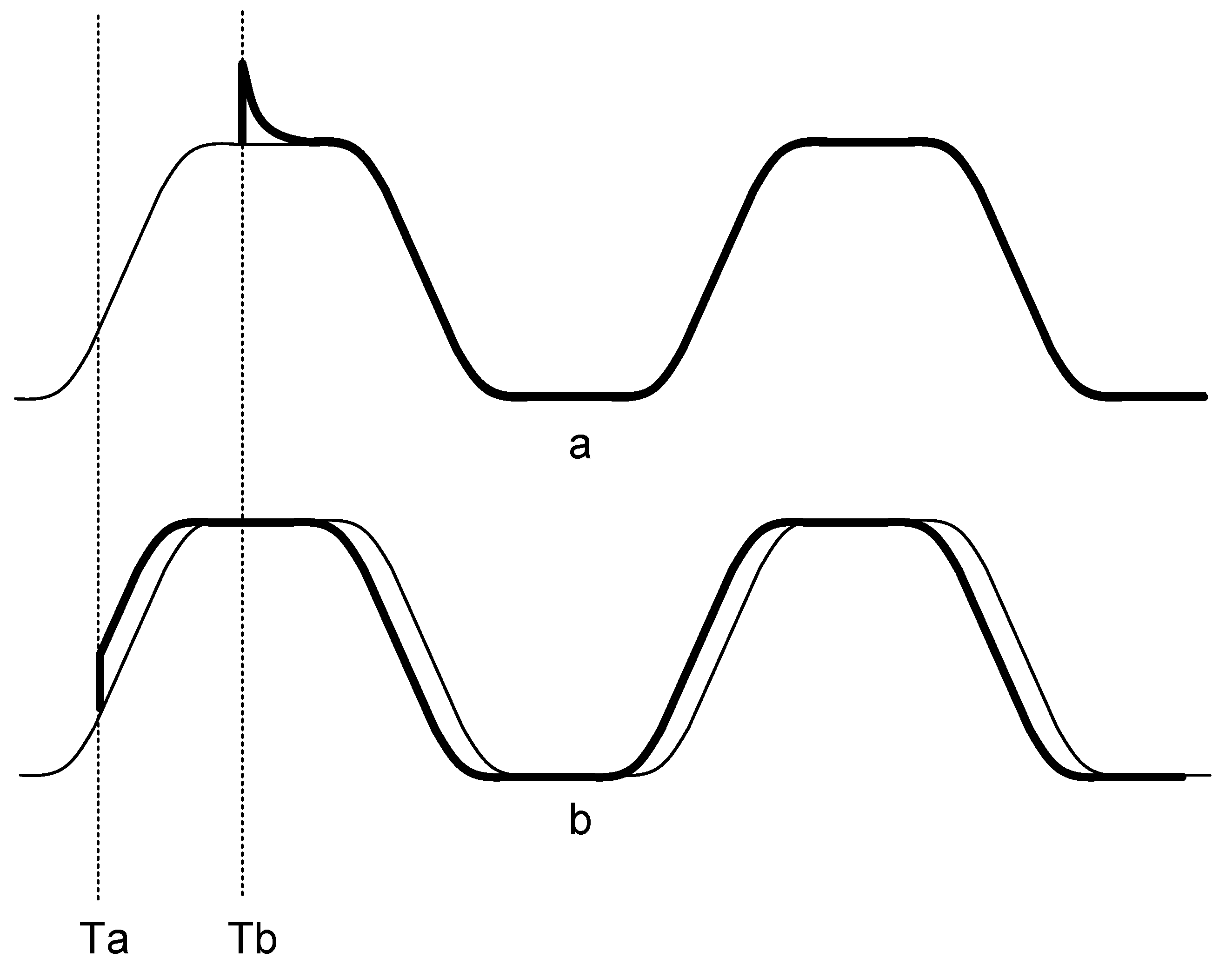
Figure 3.
VCO circuit diagram: (a) VCO delay stage; and (b) VCO common bias circuit.

Figure 4.
VCO delay cell layout.

Figure 5.
Full VCO delay cell layout with indicated laser points.

Figure 6.
Simulated results of the ring oscillator circuit. (a) Simulated Waveforms of the prototyped oscillator; (b) Simulated ISF of the prototyped oscillator.
Figure 6.
Simulated results of the ring oscillator circuit. (a) Simulated Waveforms of the prototyped oscillator; (b) Simulated ISF of the prototyped oscillator.

Figure 7.
Measurement Setup.

Figure 8.
Experimental laser facility setup. (a) Photograph of the experimental laser setup; (b) Picture of the ring oscillator layout during laser experiments.
Figure 8.
Experimental laser facility setup. (a) Photograph of the experimental laser setup; (b) Picture of the ring oscillator layout during laser experiments.

Figure 9.
Measured ISF with collected data points ().

Figure 10.
Measured ISF at four stages.

Figure 11.
Comparison between NMOS-PMOS sensitivity of a ring oscillator stage.

© 2019 by the authors. Licensee MDPI, Basel, Switzerland. This article is an open access article distributed under the terms and conditions of the Creative Commons Attribution (CC BY) license (http://creativecommons.org/licenses/by/4.0/).
Share and Cite
MDPI and ACS Style
Prinzie, J.; De Smedt, V. Single Event Transients in CMOS Ring Oscillators. Electronics 2019, 8, 618. https://doi.org/10.3390/electronics8060618
AMA Style
Prinzie J, De Smedt V. Single Event Transients in CMOS Ring Oscillators. Electronics. 2019; 8(6):618. https://doi.org/10.3390/electronics8060618
Chicago/Turabian StylePrinzie, Jeffrey, and Valentijn De Smedt. 2019. "Single Event Transients in CMOS Ring Oscillators" Electronics 8, no. 6: 618. https://doi.org/10.3390/electronics8060618
Note that from the first issue of 2016, this journal uses article numbers instead of page numbers. See further details here.