Optimization of the Cell Structure for Radiation-Hardened Power MOSFETs
by
 ,
,
Teng Wang
1, 
Xin Wan
2,3,*,
Hu Jin
2,
Hao Li
2,
Yabin Sun
4,
Renrong Liang
5,
Jun Xu
3,5 and
Lirong Zheng
1 1
School of Information Science and Technology, Fudan University, Shanghai 200433, China
2
Aurorachip Co. Ltd., Zhejiang 314000, China
3
Center for High Reliability Power Semiconductor, Yangtze Delta Region Institute of Tsinghua University, Zhejiang 314000, China
4
School of Information Science Technology, East China Normal University, Shanghai 200241, China
5
Institute of Microelectronics, Tsinghua University, Beijing 100084, China
*
Author to whom correspondence should be addressed.
Electronics 2019, 8(6), 598; https://doi.org/10.3390/electronics8060598
Submission received: 16 March 2019
/
Revised: 23 May 2019
/
Accepted: 25 May 2019
/
Published: 28 May 2019
(This article belongs to the Special Issue Radiation Tolerant Electronics)
Abstract
:Power MOSFETs specially designed for space power systems are expected to simultaneously meet the requirements of electrical performance and radiation hardness. Radiation-hardened (rad-hard) power MOSFET design can be achieved via cell structure optimization. This paper conducts an investigation of the cell geometrical parameters with major impacts on radiation hardness, and a rad-hard power MOSFET is designed and fabricated. The experimental results validate the devices’ total ionizing dose (TID) and single event effects (SEE) hardness to suitably satisfy most space power system requirements while maintaining acceptable electrical performance.
1. Introduction
Power MOSFETs are widely applied in space power systems [1]. However, they are vulnerable to particle from galactic cosmic rays, solar flares, and radiation belts, which may cause total ionizing dose effects, single event gate rupture (SEGR) effects and single event burnout (SEB) effects [2,3]. There has been a substantial research on such radiation effects [4,5,6,7], whereas radiation hardening on power MOSFETs, the more necessary resolve, has only been discussed in a few articles [8,9,10,11,12] whose content mostly focused on a single hardening issue, such as SEB, SEGR, and TID. Apparently, these radiation effects, along with electrical performance, are essential considerations during the design and fabrication stage of a power MOSFET; moreover, many trade-offs should be decided when balancing between several electrical parameters and radiation survivability. This paper entails a description of the design and fabrication of TID-, SEB-, and SEGR-hardened power MOSFETs, on the basis of a careful optimization of the devices’ cell structure and doping profile. Experimental verifications conducted show excellent radiation hardness and acceptable electrical performance of such devices for space power systems.
2. Design Considerations
2.1. Cell Structure
A power MOSFET chip is composed of several regions, including cell region, termination structure, gate bus, and gate pad. Of these, the cell region determines many electrical parameters and typically accounts for the majority of the chip area. However, it is also the most vulnerable region to irradiation. Normally, SEGR, SEB, and TID effects should be simultaneously mitigated in the cell region, whereas in other regions, only one of these effects is considered.
The cell structures and geometrical parameters of a power MOSFET are detailed in classic textbooks on power semiconductors [13,14]. Such geometrical parameters, together with the doping profiles, determine most of the device’s electrical parameters, such as on-resistance (Ron), threshold voltage (Vth), and breakdown voltage (BVds). Nonetheless, the present study does not consider detailed discussions regarding the effect of these parameters on the performance of the device. However, the electrical performance must be reasonably reserved when radiation-hardened power MOSFETs are designed.
2.2. Oxide Thickness
Gate oxide thickness is affected by three major factors, namely threshold voltage, SEGR effects and TID effects, and secondary factors as device capacitance and electro-static discharge (ESD) robustness. TID effects are mitigated by keeping the gate oxide as thin as possible [15]. Conversely, a thin gate oxide exhibits a reduced ability to withstand the SEGR effects [16]. Most power MOSFETs are designed within a pre-irradiation threshold voltage (Vth) of 2–4 V. Certain radiation hardness requires Vth to remain within such specifications after receiving a specified dose, followed by high-temperature annealing. On this basis, the chosen Vth is greatly influenced by the shifting behaviors. The shifts could be negative or positive, depending on the dominant type of radiation-induced charge [15]. For negative-shifting-dominated cases, a higher Vth can save additional room for Vth shifting and is thus preferred. By contrast, for positive-shifting-dominated cases, a lower Vth is preferred for the same reason. Once the gate oxide tOX is given, Vth can be adjusted by changing the doping density in the channel region.
Likewise, SEGR effects are mitigated by keeping the tOX large enough to avoid dielectric breakdown. During a heavy ion strike, the dielectric strength is temporarily reduced. Models with more physical insight were proposed by Javanainen et al. [17], although a simple empirical expression with little physical justification is adopted in this work, as follows [16]:
where ECRIT is the critical electric field of gate oxide that must withstand heavy-ion injection; EBD is the intrinsic dielectric breakdown strength of gate oxide, which is 107 V/cm for most thermal oxides; and Z is the atomic number of the injected heavy ions.
In rad-hard power MOSFETs’ datasheets, SEE resistance ability is illustrated as a safe operating area under certain heavy-ion injection (SEE SOA) [18,19]. In principle, SEE SOA is expressed as a series of gate and drain voltage bias conditions. The negative gate bias is directly applied to the gate to contribute all its value to the gate dielectrics, whereas only a portion of the drain bias is coupled to the gate dielectrics after heavy-ion injection [20]. Therefore, the minimum gate oxide bounded by SEGR effects can be calculated as follows:
where α is the coupled ratio of drain voltage related to the device design, as discussed later. Note that the bias conditions considered here are the worst bias conditions for SEGR production and are, hence, used for SEGR testing. The shift in the threshold voltage due to TID effects is a major problem for all metal-oxide-semiconductor (MOS) devices. For power MOSFETs, the relatively thick gate oxide makes this issue more severe. The Vth shift has been attributed to two kinds of radiation-induced charges, namely oxide charges and interface traps [15]. Therefore, the Vth shift (ΔVth) is the sum of the oxide-charge-induced negative shift, named ΔVot, and the interface-trap-induced positive shift, named ΔVit. Both ΔVot and ΔVit are strongly related to tOX. The relationship can be expressed as follows [21]:
where ρot,it is the charge distribution of radiation-induced oxide-trapped or interface-trapped charge. Reduction of tOX entails a two-fold effect. First, reducing tOX can reduce the Vth shift for a given charge density, which is attributed to a larger COX resulting from a thinner tox. Second, it can reduce charge generation for a given dose, as shown in Equation (3). The integration term can be simplified by introducing a uniform charge generation for the oxide charge, resulting in the expression [22]:
where q is the electric charge (expressed in Coulomb), g0 is the electron–hole pair generation rate in SiO2 (in pairs/cm3/rad(SiO2)), D is the total dose level in units of rad(SiO2), Yh is charge yield of holes, σh is trapping cross section for holes captured by hole traps in oxide, and εOX is the dielectric constant of SiO2. Note that Y and σ are affected by the electric field presented during irradiation, and the trapped charges can also be annealed with elevated temperature.
Interface traps generation is much more complicated. However, protons are considered to play a key role in the formation of interface traps. Moreover, the process of proton generation in the oxide is intimately related to the transport of holes. By introducing the parameter Yp, which is the product of ND’H (concentration of hydrogen-containing defects) and σD’H (cross section for proton release from these defects) [23], ΔVit can be expressed in a similar manner as ΔVot, as follows:
where σp is the cross section of protons captured by the traps at interface. Note that for one to get a relatively simple solution, a uniform distribution of ND’H (and, hence, the Yp) in terms of space has been assumed, which may not be true for all cases. Moreover, ND’H is space-and-time-dependent and σp is field-dependent. Therefore, a simple method for quantitatively calculating the radiation-induced interface traps for all cases seems impractical, if not impossible. However, as an analytical model, Equation (5) does reflect the relationship of the interface trap generation with the hole transport, as widely accepted by society. Combining Equations (4) and (5) allows the maximum tOX bounded by the TID effects to be expressed as follows:
where ΔVth,max is the maximum allowed threshold shift. Note that even for a given dose, |Ypσp − σh| varies with dose rate, bias condition, and temperature and is strongly related to the fabrication process. Given this limitation and the uncertainties, |Ypσp − σh| remains a useful parameter to be extracted from the experimental perspective and can thus be used as a starting point in the device’s design. Manipulating Equations (2) and (6) yields the lower and upper bounds of tOX. Once tOX is chosen, channel doping density can be fixed with equations governing Vth.
2.3. JFET Region Width
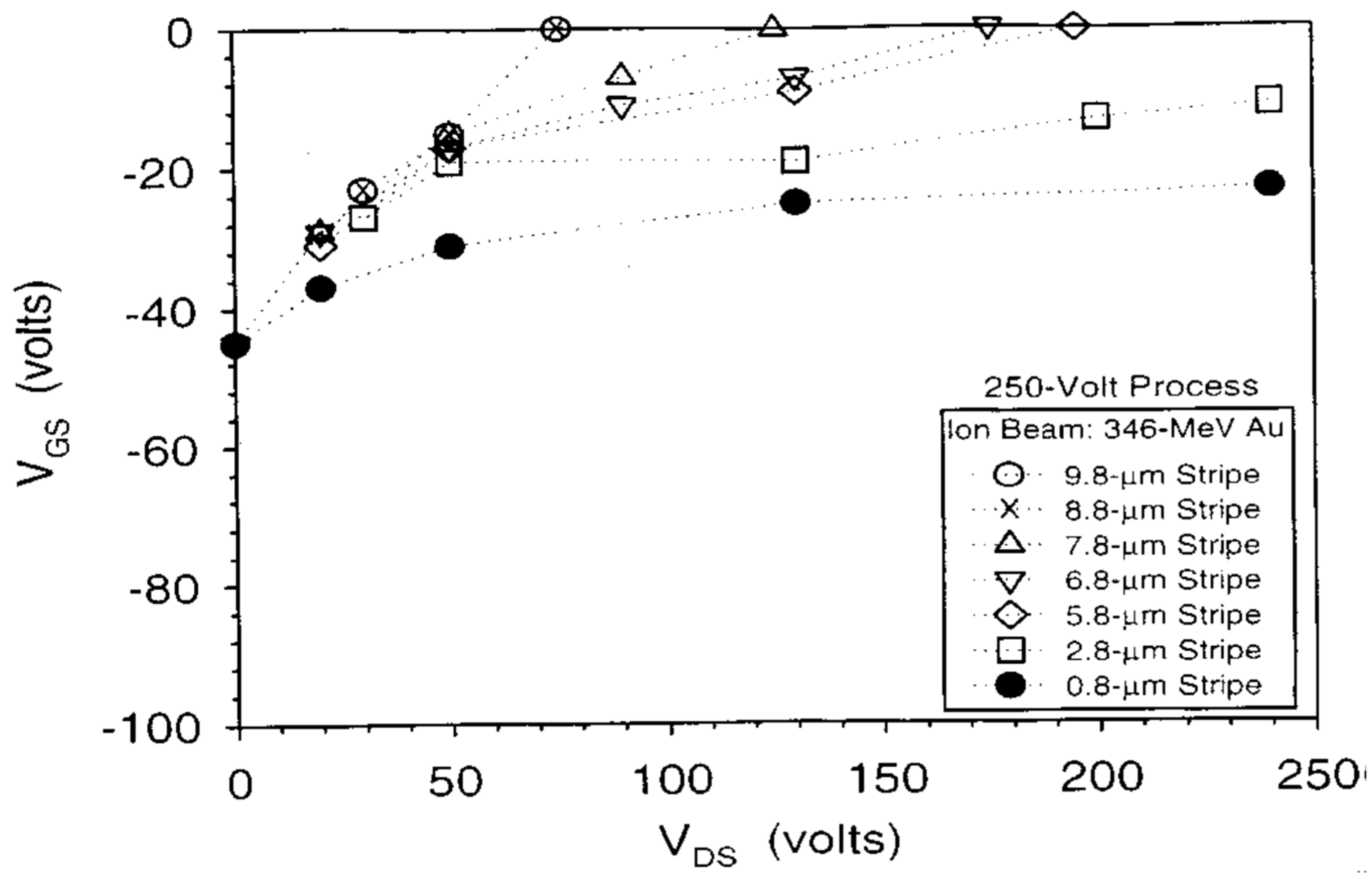
Parameter α has been introduced in Section 2.2 to account for the coupling of drain voltage to the gate dielectric. Based on Equation (2), the lower bound of tOX can be reduced with reduced α, which means that a larger range of tOX is available at the design stage. Moreover, α has been demonstrated to correlate with JFET region width (LJFET) and thus can be reduced, with a reduced LJFET [10], as illustrated in Figure 1.
Although it greatly improves SEGR hardness, a small LJFET creates a negative impact on Ron. The specific resistance contributed by the JFET region (RJFET,SP) can be expressed as follows:
where ρJFET is the resistivity of the JFET region, which is inversely proportional to JFET region doping; HJP is body junction depth; LCELL is the cell pitch; and LJFET is the JFET region width. According to Equation (7), RJFET,SP is inversely proportional to LJFET; thus, decreasing LJFET will greatly increase RJFET,SP, leading to worse resistance. Fortunately, the JFET region’s resistance is only a portion of the total resistance. Therefore, the increasing on-resistance can be tolerated, as long as LJFET is not extremely small. Nevertheless, the chosen LJFET remains a critical element. A previous study [10] asserted that for 250 V power MOSFETs, LJFET should be less than 5.8 µm to achieve a full VDS range under zero gate bias. The JFET region should be carefully designed for SEGR-hardened devices.
2.4. P Body and P+ Well Doping
Several models have been proposed to describe the SEB process [24,25,26]. For instance, the parasitic BJT has been postulated to play a key role in SEB production. With the P-body region of the power MOSFET acting as the base region of the parasitic BJT, the body’s doping profile becomes essential for hardening the device against SEB effects. In general, larger P-body depth (HJP) and higher doping concentrations (NBODY), as well as a reduced length between N+ source edge and P+ well edge (LBODY), are desirable for an SEB-hardened cell design. However, as expressed in Equation (7), a deeper P-body has negative effects on RJFET,SP, whereas a high NBODY or a short LBODY may affect the channel doping concentration.
3. Results
TID- and SEE-hardened power MOSFETs were designed on account of the trade-offs mentioned above. The key geometrical parameters and doping concentrations essential for the design are summarized in Table 1. Buffer layer technology was employed to improve SEB hardness [11]. The values of other parameters were chosen as common non-rad-hard power MOSFET designs. The whole chip area was 12 mm2, whereas the active area (cell region) was approximately 8.5 mm2. Stripe cell topology [10] was considered.
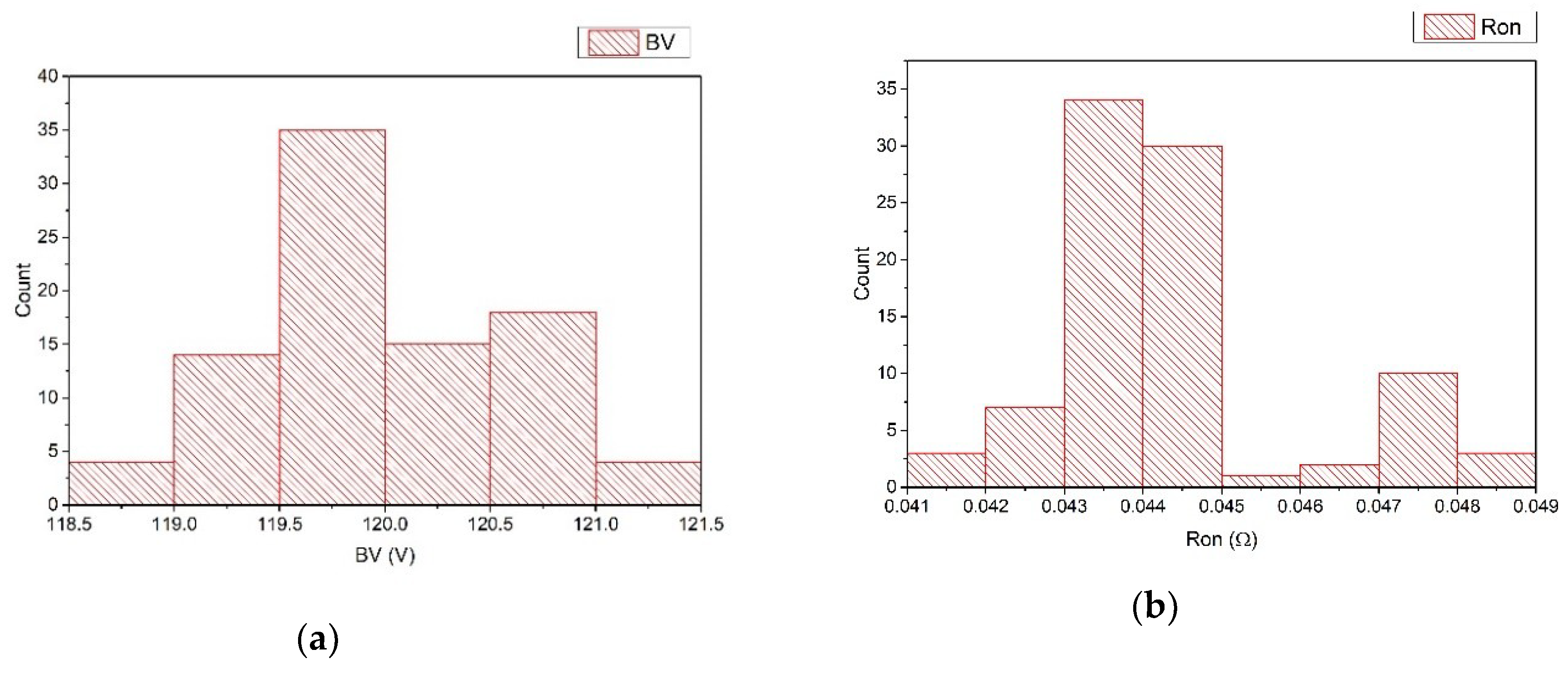
The designed power MOSFETs were fabricated by Tianjin Zhonghuan Semiconductor Co., Ltd., with 6-inch wafers. Processes with high thermal budget, such as the P-body driven process, were adjusted prior to gate oxidation to improve TID hardness. Diced devices were packaged in TO-220. Ninety devices were randomly selected for testing under a Keysight B1506 power semiconductor analyzer. Figure 2 illustrates the distributions of the testing results, with median BVds around 120 V and median Ron around 44 mΩ. For this cell design, for a 120 V maximum blocking ability, the specific resistance was 3.74 mΩ-cm2. All the Vth values fell in the range of 2.36–2.62 V, of which more than 80% were roughly 2.40–2.50 V (not depicted in the figure). The ESD endurance exceeded 2000 V in human body model (HBM) mode, and the maximum avalanche energy was 662.5 mJ.
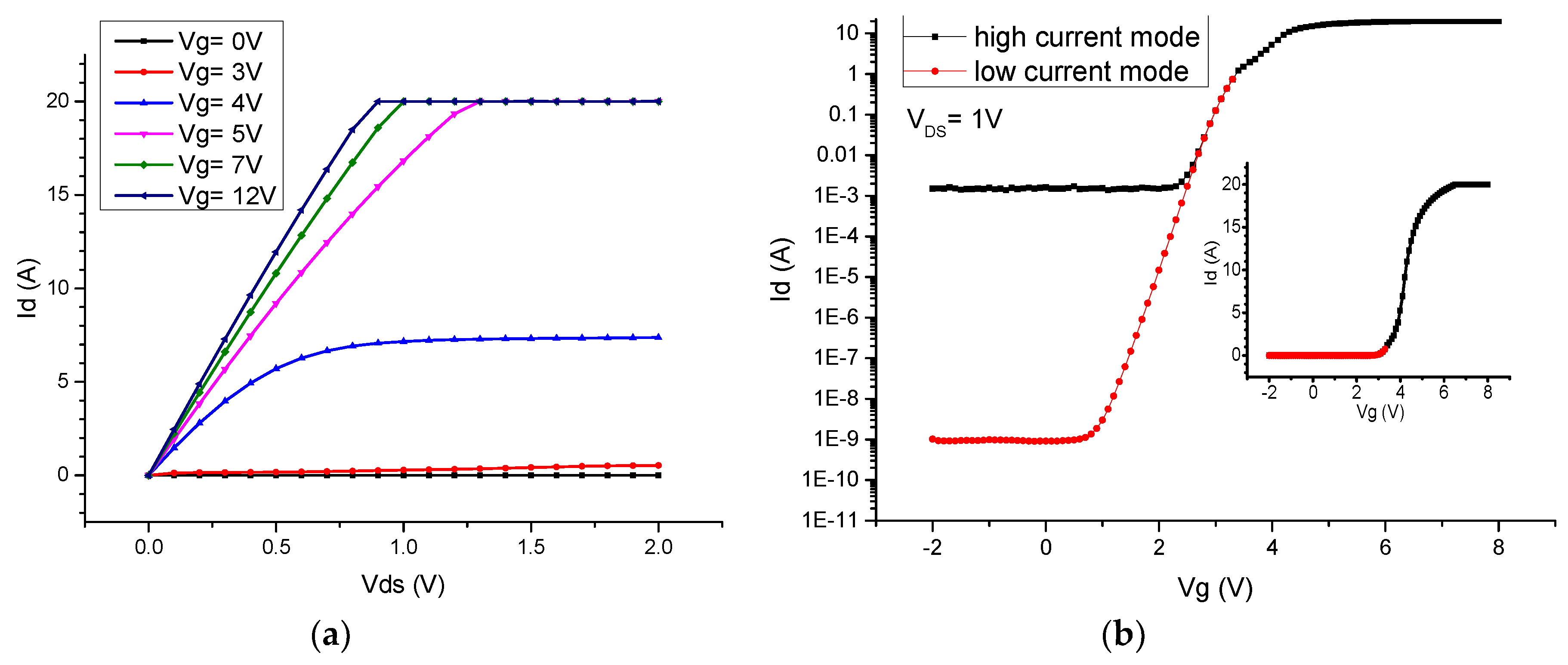
Figure 3 illustrates the typical output and transfer curves, as measured with the Keysight B1506. The B1506 testing system has two modes, namely high-current and low-current modes. On the one hand, the high-current mode is able to test current up to 20 A; the plateau is caused by this limitation. However, this mode is not suitable for testing low current because of the leakage issue. On the other hand, the low-current mode is able to test current under a picoampere, although the maximum current in this mode is 1 A. The transfer curves in Figure 3 combined the results for both testing modes.
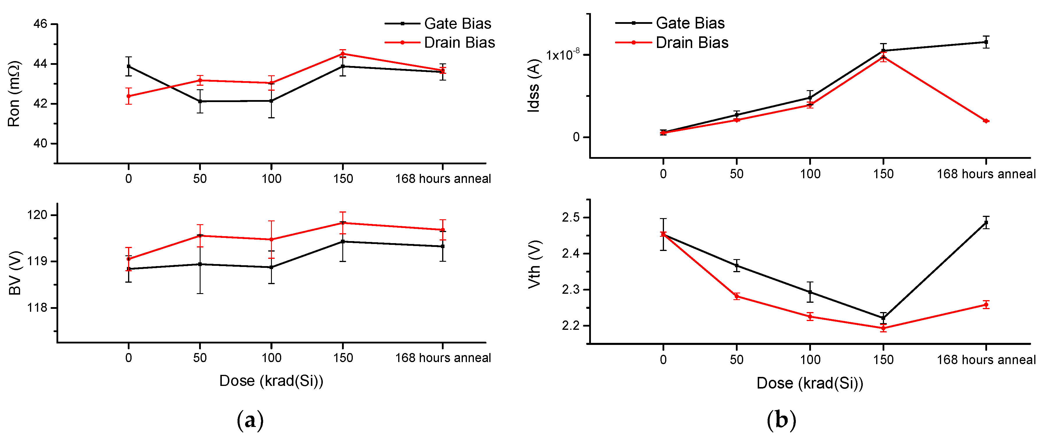
The fabricated devices were irradiated with Co-60 at the Shanghai Institute of Applied Physics, Chinese Academy of Sciences. The devices were placed on especially designed PCB boards, allowing separately the gate and drain node biases. The PCB boards were separated from the radiation source by approximately 30 cm, thus yielding a calculated dose rate of 100 rad(Si)/s. Additionally, the PCB boards were made to be as small as possible to minimize the dose rate inhomogeneous. Subsequently, the devices were irradiated under room temperature and then annealed at 100 °C for 168 h under the same bias condition after irradiation. For the gate bias condition (GB), the gate was biased at 12 V, with the drain and the source connected to ground. For the drain biased condition (DB), the drain was biased at 80 V, with the gate and the source connected to ground. Three devices were tested under each bias condition. Results of the TID experiment are displayed in Figure 4.
Based on the figure, the on-resistance and breakdown voltage indicated negligible change after 150 krad(Si) TID irradiation and 168 h annealing, for both bias conditions. Idss also increased with the dose for GB and DB, whereas Idss increased after annealing under GB and consequently decreased under DB. For the threshold voltage, Vth decreased with the dose for both bias conditions, but with different annealing behavior. More specifically, Vth rebounded to a value slightly higher than its initial value under GB, whereas the rebound was much less under DB. Nonetheless, for each bias condition, at 150 krad(Si) dose, the annealing-induced Vth shift was less than 0.25 V. The shift behaviors of Vth during irradiation and annealing are described further under the discussion section. The terminations used in these devices included a traditional floating ring and filed plate structure, with optimized parameters [9]. The small BVds and Idss change (Figure 4) indicate that the design of the termination was also radiation-hardened.
SEE experiments were conducted at Institute of Modern Physics, Chinese Academy of Sciences. The chips were packaged in TO-39, with the cap removed. 794 MeV Xe ions with a surface linear energy transfer (LET) of approximately 66 MeV·cm2/mg were used. During the experiment, VGS was set to 0 V, and VDS was increased in steps of 10 V. The flux was roughly within 5000–10,000 ions/cm2s; the pass criteria was both gate and drain leakage current stay within the specification value after 2 × 10⁶ ions/cm2 irradiation [19]. Neither SEB nor SEGR was observed under VDS = 100 V with a VGS = 0 V bias condition.
4. Discussion
In space applications, the dose rate is much lower than the high-dose rate (HDR) experiment typically performed in laboratory. Such disparity may cause a significant difference of |Ypσp − σh| used in Equation (6) in the two cases. However, low-dose rate (LDR) experiments are relatively time-consuming and expensive. Therefore, the present study adopted an accelerated aging test to estimate the worst-case degradation of MOS devices [27,28], as it has been proven applicable to power MOSFETs [29]. Initially, the devices were irradiated with HDR for a relatively short time. Since the interface traps took a longer time to form, hole trapping in oxide defects dominated in this stage, thereby yielding |Ypσp − σh| ≈ σh and a negative ΔVth. In the annealing stage, the build-up of interface traps dominated while the trapped oxide charges decreased with time, yielding a recovery or even a rebound of ΔVth. Therefore, the HDR+ high-temperature annealing procedure eliminated charge compensation in the LDR environment and produced worse (conserved) results. To further investigate the details of the behavior of radiation-induced charges, a mid-gap method was used to separate these two charges [30,31], where VT is the threshold voltage extracted by using the maximum transconductance method. Here, note that VT was different from Vth in Figure 4b, which was basically the gate voltage as the drain current reached 1 mA. Therefore, it was convenient for the engineer to monitor Vth. On the other hand, VT has a physical meaning and is more accurate for parameter calculation. The mobility was extracted as follows:
where ID(sat) is drain current in the saturation region, W is the total channel width, L is the channel length, and COX is the gate oxide capacitance. Since Figure 4 depicts that the sample-to-sample variations were acceptable, a single device was randomly selected to perform extraction for each bias condition. Table 2 presents the extracted parameters of the device pre-irradiation, at 150 krad(Si) irradiation, and after annealing.
The TID-induced oxide-charge density was 1.86 × 1011 cm−2 for the drain bias condition, whereby such oxide charges should lead to a −0.69 V VT shift. However, the negative shift was partially compensated by an interface-trap-induced positive shift, resulting in a net shift of −0.14 V. For the GB, both ΔNot and ΔNit were 30% less than those for the DB. During the annealing process, almost half the generated oxide charges were reduced for both bias conditions. Nevertheless, the annealing behaviors of Nit for both conditions were different; Nit increased by approximately 10% for the GB and reduced by roughly 75% for the DB. Such similarity between Nit and Idss during the annealing stage indicates that the increasing trend for Idss might be related to the generation of interface traps. Moreover, as expected, the Nit generation and annealing was qualitatively consistent with the extracted mobility value [32]. The data in Table 2 can be used to calculate Ypσp and σh, as a starting point in the device design. However, these parameters are highly process-dependent and are, therefore, only valid for this specific process flow.
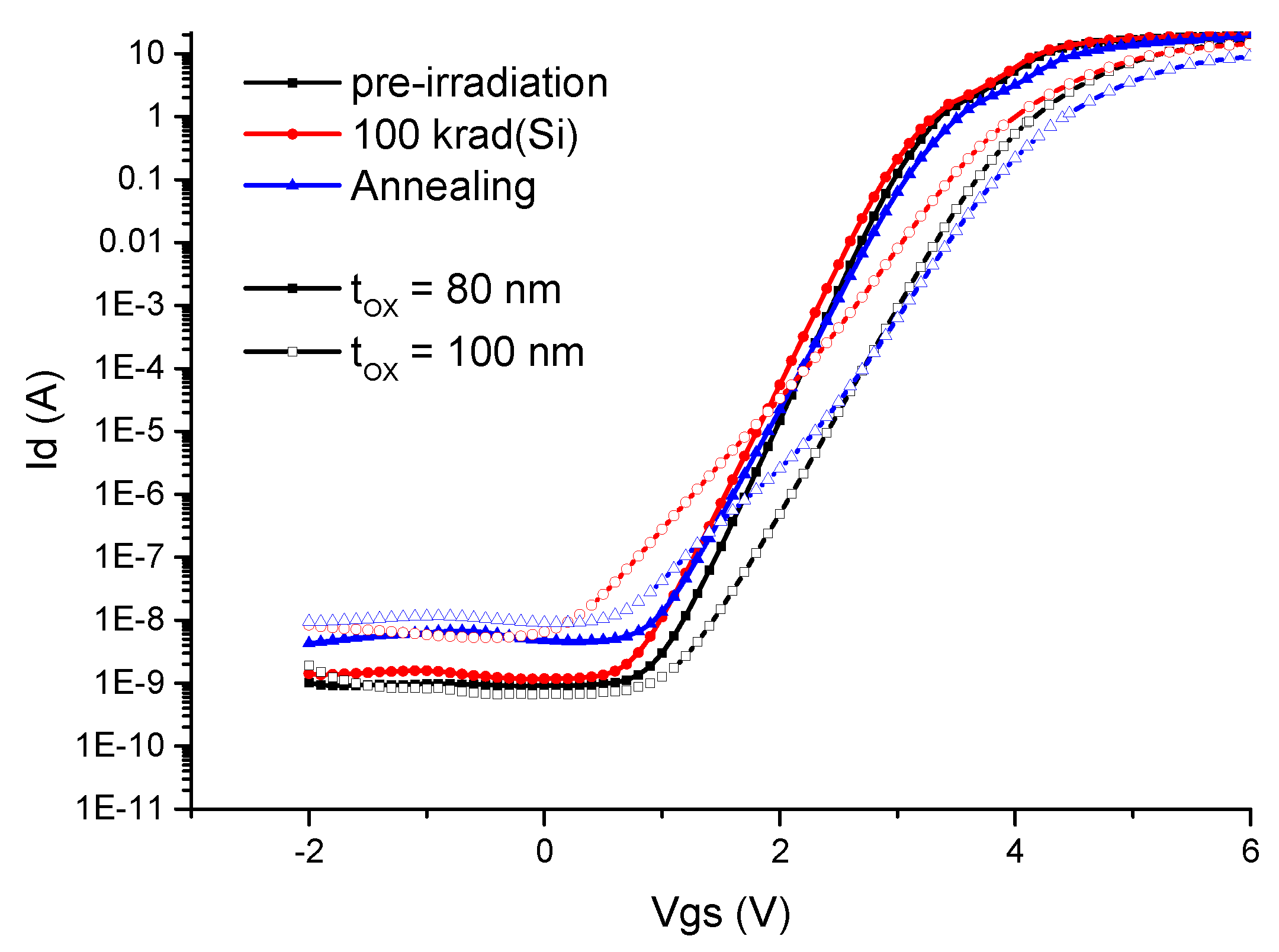
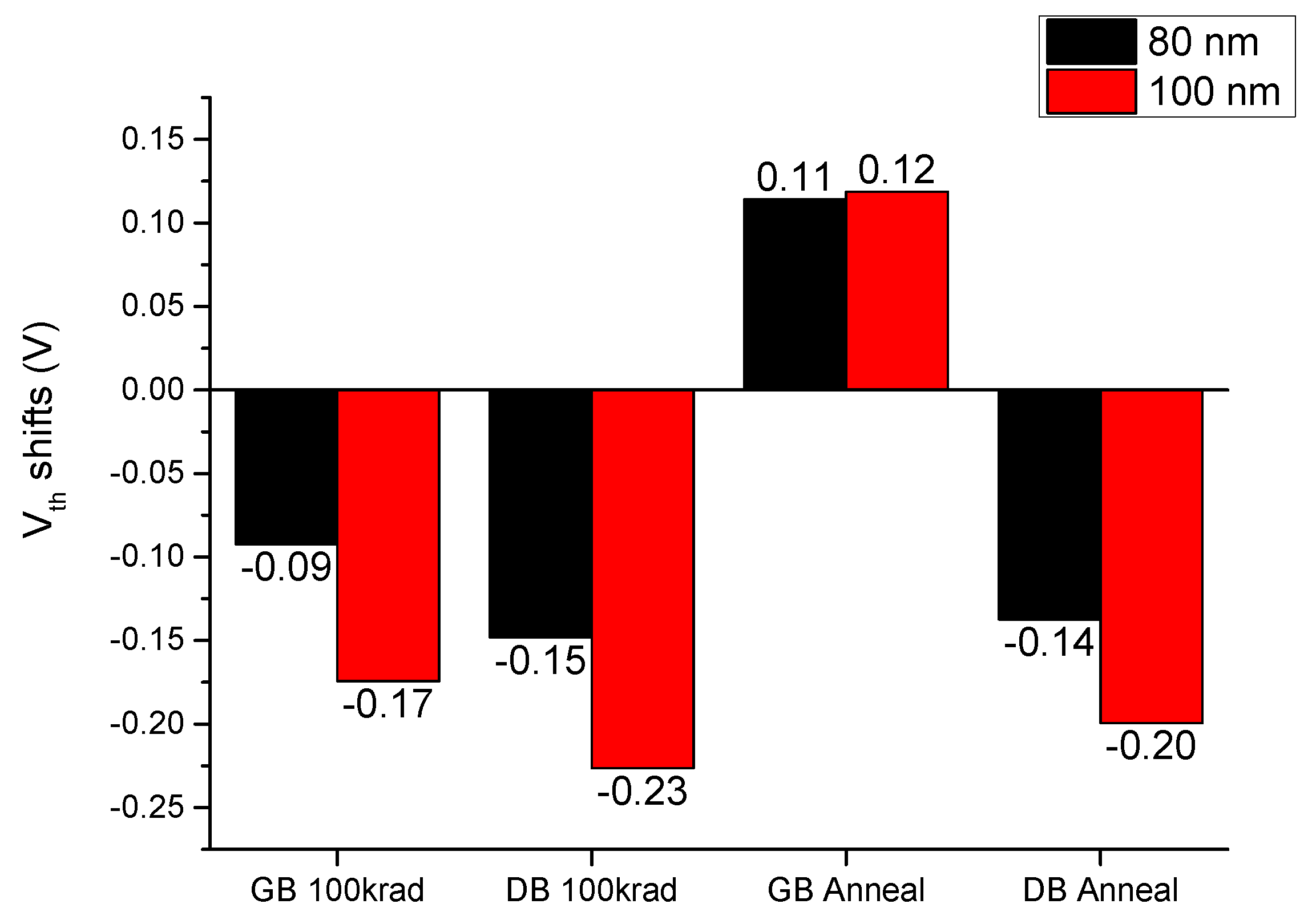
The parameter selection was further evaluated through fabrication of devices with tOX = 100 nm, which were later subjected to TID experiments. For the other geometric parameters, the process flow and TID experiment setups were kept the same as those for the 80 nm samples. However, note that the oxidation time for the 100 nm samples was longer; thus, worse TID hardness could be expected because of the larger thermal budget and thicker tOX, as illustrated in Figure 5. Here, the bias condition was the same as the gate bias condition described in Section 3. Much larger negative shifts and significant twists in the figure indicate both oxide charges and interface traps being much more in the 100 nm oxide thickness. Figure 6 illustrates the VT shifts under the two bias conditions after 100 krad irradiation and annealing, where the shifts were higher with thicker tOX, thus reflecting better SEGR hardness. A comparison of SEGR hardness of these devices is a future direction relative to the present study.
5. Conclusions
A rad-hard power MOSFET is appropriately designed through consideration of several radiation effects as TID, SEB, and SEGR, as well as a balance among electrical parameters as Ron, Vth and BVds. In this work, the effects of cell structure adjustment on the performance of a power MOSFET were examined, by first analyzing the design parameters. Next, a SEE- and TID-hardened power MOSFET was designed and fabricated by implementing the accompanying design rules. Results of the investigation confirmed the achievement of excellent radiation hardness and decent specific on-resistance for the device. Technically, the Vth shifts were less than 0.25 V for 150 krad(Si) irradiation and 168 h annealing. No SEE was observed under VGS = 0 V and the VDS = 100 V bias condition with LET = 66 MeV·cm2/mg under Xe ion irradiation. Further investigation on the TID experimental results indicated the estimated charge density induced by radiation and annealing. Moreover, devices with thicker gate oxide were fabricated as the counterpart for the parameter selection evaluation. Experiments with these devices showcased their great potential for application in space power systems.
As a general rule, radiation environments are different for various mission orbits. Notably, a spacecraft in van-Allen belts would suffer more from a TID effect, whereas a deep space mission would require high SEE-hardness devices. Additionally, devices in low-Earth orbits requires lower radiation hardness while they are expected to exhibit better electrical parameters. Hence, various devices with different electrical parameters and radiation hardness are required for different missions. The results in the present study provide an insight for the power semiconductor designer to balance the parameters involved and to design power MOSFET devices based on the application requirements.
Author Contributions
Conceptualization, methodology, writing—original draft preparation, T.W. and X.W.; Chip design, H.J.; Chip fabrication, H.L.; TID and SEE experiment, T.W.; Data analysis, Y.S.; Writing—review and editing, R.L. and J.X.; Supervision, J.X. and L.Z.; Resources and funding acquisition, L.Z.
Funding
This research received no external funding.
Acknowledgments
The authors would like to thank Wanli Wang and Xiaofang Li from Tianjin Zhonghuan Semiconductor Co., Ltd. for their help on device fabrication.
Conflicts of Interest
The authors declare no conflicts of interest. The funders had no role in the design of the study; in the collection, analyses, or interpretation of data; in the writing of the manuscript, or in the decision to publish the results.
Nomenclature
| Symbol | Description | Equation |
| ECRIT | Critical electric field of gate oxide that must withstand heavy-ion injection | (1) |
| VGS | Applied gate voltage | (1) |
| tOX | Gate oxide thickness | (1) |
| EBD | Intrinsic dielectric breakdown strength | (1) |
| Z | The atomic number of the injected heavy ions | (1) |
| tOX,min | The minimum gate oxide bounded by single event gate rupture (SEGR) effects | (2) |
| α | The coupled ratio of drain voltage | (2) |
| VDS | Applied drain voltage | (2) |
| ΔVot,it | Threshold shifts induced by oxide-charge or interface traps | (3) |
| COX | Gate capacitance | (3) |
| ρot,it | The charge distribution of radiation-induced oxide-trapped or interface-trapped charge | (3) |
| ΔQot | Radiation-induced charges in oxide | (4) |
| q | Electric charge | (4) |
| g0 | Electron–hole pair generation rate in SiO2 | (4) |
| D | The total dose level | (4) |
| Yh | Charge yield of holes | (4) |
| σh | Trapping cross section for holes captured by hole traps in oxide | (4) |
| εOX | The dielectric constant of SiO2 | (4) |
| ΔQit | Radiation-induced interface trap charges | (5) |
| Yp | Product of concentration of hydrogen-containing defects and cross section for proton release from these defects | (5) |
| σp | The cross section of protons captured by the traps at interface | (5) |
| tOX,max | The maximum gate oxide bounded by total ionizing dose (TID) effects | (6) |
| ΔVth,max | The maximum allowed threshold shift | (6) |
| RJFET,SP | Specific resistance contributed by the JFET region | (7) |
| ρJFET | The resistivity of the JFET region | (7) |
| HJP | Body junction depth | (7) |
| LCELL | Cell pitch | (7) |
| LJFET | JFET region width | (7) |
References
- Adell, P.C.; Scheick, L.Z. Radiation Effects in Power Systems: A Review. IEEE Trans. Sci. 2013, 60, 1929–1952. [Google Scholar] [CrossRef]
- Barth, J.; Gee, G.; Adolphsen, J.W. First observation of proton induced power MOSFET burnout in space: The CRUX experiment on APEX. IEEE Trans. Sci. 1996, 43, 2921–2926. [Google Scholar]
- George, J.S.; Clymer, D.A.; Turflinger, T.L.; Mason, L.W.; Stone, S.; Koga, R.; Beach, E.; Huntington, K.; Lauenstein, J.-M.; Titus, J.; et al. Response Variability in Commercial MOSFET SEE Qualification. IEEE Trans. Sci. 2017, 64, 317–324. [Google Scholar] [CrossRef]
- Kuboyama, S.; Mizuta, E.; Nakada, Y.; Shindou, H. Physical analysis of damage sites introduced by SEGR in silicon vertical power MOSFETs and implications for post-irradiation gate-stress test. IEEE Trans. Nucl. Sci. 2019, in press. [Google Scholar] [CrossRef]
- Singh, G.; Galloway, K.F.; Russell, T.J. Radiation-Induced Interface Traps in Power Mosfets. IEEE Trans. Sci. 1986, 33, 1454–1459. [Google Scholar] [CrossRef] [Green Version]
- Picard, C.; Brisset, C.; Hoffmann, A.; Charles, J.-P.; Joffre, F.; Adams, L.; Siedle, A.H. Use of electrical stress and isochronal annealing on power MOSFETs in order to characterize the effects of 60 Co irradiation. Microelectron. Reliab. 2000, 40, 1647–1652. [Google Scholar] [CrossRef]
- Titus, J.L. An Updated Perspective of Single Event Gate Rupture and Single Event Burnout in Power MOSFETs. IEEE Trans. Sci. 2013, 60, 1912–1928. [Google Scholar] [CrossRef]
- Roper, G.B.; Lowis, R. Development of a radiation hard n-channel power MOSFET. IEEE Trans. Nucl. Sci. 1983, 30, 4110–4115. [Google Scholar] [CrossRef]
- Davis, K.; Schrimpf, R.; Cellier, F.; Galloway, K.; Burton, D.; Wheatley, C. The effects of ionizing radiation on power-MOSFET termination structures. IEEE Trans. Sci. 1989, 36, 2104–2109. [Google Scholar] [CrossRef] [Green Version]
- Savage, M.; Burton, D.; Wheatley, C.; Titus, J.; Gillberg, J. An improved stripe-cell SEGR hardened power MOSFET technology. IEEE Trans. Sci. 2001, 48, 1872–1878. [Google Scholar] [CrossRef]
- Liu, S.; Titus, J.L.; Boden, M. Effect of Buffer Layer on Single-Event Burnout of Power DMOSFETs. IEEE Trans. Sci. 2007, 54, 2554–2560. [Google Scholar] [CrossRef]
- Wan, X.; Zhou, W.S.; Ren, S.; Liu, D.G.; Xu, J.; Bo, H.L.; Zhang, E.X.; Schrimpf, R.D.; Fleetwood, D.M.; Ma, T. SEB Hardened Power MOSFETs With High-K Dielectrics. IEEE Trans. Sci. 2015, 62, 2830–2836. [Google Scholar] [CrossRef]
- Baliga, B.J. Advanced Power MOSFET Concepts; Springer: New York, NY, USA, 2010; pp. 23–61. [Google Scholar]
- Grant, D.A.; Gowar, J. Power MOSFETs: Theory and Applications, 1st ed.; Wiley-Interscience: New York, NY, USA, 1989. [Google Scholar]
- Schrimpf, R.; Wahle, P.; Andrews, R.; Cooper, D.; Galloway, K. Dose-rate effects on the total-dose threshold-voltage shift of power MOSFETs. IEEE Trans. Sci. 1988, 35, 1536–1540. [Google Scholar] [CrossRef]
- Titus, J.; Wheatley, C.; Van Tyne, K.; Krieg, J.; Burton, D.; Campbell, A. Effect of ion energy upon dielectric breakdown of the capacitor response in vertical power MOSFETs. IEEE Trans. Sci. 1998, 45, 2492–2499. [Google Scholar] [CrossRef]
- Javanainen, A.; Ferlet-Cavrois, V.; Jaatinen, J.; Kettunen, H.; Muschitiello, M.; Pintacuda, F.; Rossi, M.; Schwank, J.R.; Shaneyfelt, M.R.; Virtanen, A. Semi-Empirical Model for SEGR Prediction. IEEE Trans. Sci. 2013, 60, 2660–2665. [Google Scholar] [CrossRef]
- STMicroelectronics. STRH8N10 Datasheets. Available online: https://www.st.com/resource/en/datasheet/strh8n10.pdf (accessed on 3 May 2019).
- Iakovlev, S.A.; Anashin, V.S.; Chubunov, P.A.; Koziukov, A.E.; Bu-Khasan, K.B.; Maksimenko, T.A.; Chlenov, A.M. MOSFETs SEB & SEGR qualification results with SOA estimation. In Proceedings of the 17th European Conference on Radiation and Its Effects on Components and Systems (RADECS), Geneva, Switzerland, 2–6 October 2017. [Google Scholar]
- Wheatley, C.; Titus, J.; Burton, D. Single-event gate rupture in vertical power MOSFETs; an original empirical expression. IEEE Trans. Sci. 1994, 41, 2152–2159. [Google Scholar] [CrossRef]
- Schwank, J.R.; Shaneyfelt, M.R.; Fleetwood, D.M.; Felix, J.A.; Dodd, P.E.; Paillet, P.; Ferlet-Cavrois, V. Radiation effects in MOS oxides. IEEE Trans. Nucl. Sci. 2008, 55, 1833–1853. [Google Scholar] [CrossRef]
- Fleetwood, D.; Meisenheimer, T.; Scofield, J. 1/f noise and radiation effects in MOS devices. IEEE Trans. Electron Devices 1994, 41, 1953–1964. [Google Scholar] [CrossRef]
- Rashkeev, S.; Cirba, C.; Fleetwood, D.; Schrimpf, R.; Witczak, S.; Michez, A.; Pantelides, S. Physical model for enhanced interface-trap formation at low dose rates. IEEE Trans. Sci. 2002, 49, 2650–2655. [Google Scholar] [CrossRef]
- Hohl, J.H.; Galloway, K.F. Analytical model for single event burnout of power MOSFETs. IEEE Trans. Electron Devices 1994, 41, 1953–1964. [Google Scholar] [CrossRef]
- Wrobel, T.; Beutler, D. Solutions to heavy ion induced avalanche burnout in power devices. IEEE Trans. Sci. 1992, 39, 1636–1641. [Google Scholar] [CrossRef] [Green Version]
- Johnson, G.H.; Palau, J.M.; Dachs, C.; Galloway, K.F.; Schrimpf, R.D. A review of the techniques used for modeling single-event effects in power MOSFET’s. IEEE Trans. Nucl. Sci. 1996, 43, 546–560. [Google Scholar] [CrossRef]
- Department of Defense. MIL-STD-883E, Test Method 1019.4. Ionizing Radiation (Total Dose) Test Procedure; Defense Supply Center Columbus: Columbus, OH, USA, 1996. [Google Scholar]
- Department of Defense. MIL-STD-750E, Test Method 1019.5 Steady-State Total Dose Irradiation Procedure; Defense Supply Center Columbus: Columbus, OH, USA, 2006. [Google Scholar]
- Khosropour, P.; Galloway, K.F.; Zupac, D.; Schrimpf, R.D.; Calvel, P. Application of test method 1019.4 to non-hardened power MOSFETs. IEEE Trans. Nucl. Sci. 1994, 41, 555–560. [Google Scholar] [CrossRef]
- Winokur, P.S.; Schwank, J.R.; McWhorter, P.J.; Dressendorfer, P.V.; Turpin, D.C. Correlating the Radiation Response of MOS Capacitors and Transistors. IEEE Trans. Sci. 1984, 31, 1453–1460. [Google Scholar] [CrossRef]
- McWhorter, P.J.; Winokur, P.S. Simple technique for separating the effects of interface traps and trapped-oxide charge in metal-oxide-semiconductor transistors. Appl. Phys. Lett. 1986, 48, 133–135. [Google Scholar] [CrossRef]
- Zupac, D.; Galloway, K.; Khosropour, P.; Anderson, S.; Schrimpf, R.; Calvel, P. Separation of effects of oxide-trapped charge and interface-trapped charge on mobility in irradiated power MOSFETs. IEEE Trans. Sci. 1993, 40, 1307–1315. [Google Scholar] [CrossRef]
Figure 1.
Single event gate rupture (SEGR) failure threshold responses for various LJFET, after Reference [10].
Figure 1.
Single event gate rupture (SEGR) failure threshold responses for various LJFET, after Reference [10].

Figure 2.
Test results for 90 randomly selected devices: (a) Breakdown voltage results; (b) On-resistance results.
Figure 2.
Test results for 90 randomly selected devices: (a) Breakdown voltage results; (b) On-resistance results.

Figure 3.
(a) Output curves and (b) transfer curves for the fabricated devices.

Figure 4.
Parameters change with total ionizing dose (TID) dose and annealing time: (a) Ron and BVdss; (b) Idss and Vth.
Figure 4.
Parameters change with total ionizing dose (TID) dose and annealing time: (a) Ron and BVdss; (b) Idss and Vth.

Figure 5.
Subthreshold characteristics of power devices with 80 nm and 100 nm gate oxides pre- and post-irradiation and post-annealing.
Figure 5.
Subthreshold characteristics of power devices with 80 nm and 100 nm gate oxides pre- and post-irradiation and post-annealing.

Figure 6.
Threshold voltage shifts for 80 nm and 100 nm gate oxide devices under gate bias and drain bias (RB) conditions, after receiving 100-krad(Si) TID and annealing.
Figure 6.
Threshold voltage shifts for 80 nm and 100 nm gate oxide devices under gate bias and drain bias (RB) conditions, after receiving 100-krad(Si) TID and annealing.


Table 1.
Key geometrical parameters and doping concentrations for device design.
| Symbol in Figure 1 | Value | Unit |
|---|---|---|
| tox | 80 | nm |
| HJP | 3 | µm |
| LCELL | 10 | µm |
| LBODY | ~2 | µm |
| LJFET | ~3 | µm |
| NBODY | ~5 × 10¹⁶ | cm−3 |
Table 2.
Extracted parameters for device pre-irradiation.
| Unit | Virgin | 150 krad(Si) | Anneal | ||||
|---|---|---|---|---|---|---|---|
| Gate Bias | Drain Bias | Gate Bias | Drain Bias | Gate Bias | Drain Bias | ||
| VT | V | 3.75 | 3.82 | 3.61 | 3.68 | 3.88 | 3.66 |
| Vot | V | 0.96 | 0.99 | 0.45 | 0.30 | 0.68 | 0.69 |
| µn | cm2/V·s | 319.34 | 339.00 | 273.30 | 252.45 | 219.05 | 279.15 |
| ΔVT | V | 0.00 | 0.00 | −0.14 | −0.14 | 0.13 | −0.15 |
| ΔVot | V | 0.00 | 0.00 | −0.51 | −0.69 | −0.28 | −0.30 |
| ΔVit | V | 0.00 | 0.00 | 0.37 | 0.55 | 0.41 | 0.14 |
| ΔNot | cm−2 | 0.00 | 0.00 | 1.37 × 10¹¹ | 1.86 × 10¹¹ | 0.76 × 10¹¹ | 0.80 × 10¹¹ |
| ΔNit | cm−2 | 0.00 | 0.00 | 1.00 × 10¹¹ | 1.48 × 10¹¹ | 1.11 × 10¹¹ | 0.39 × 10¹¹ |
| Δµn | cm2/V·s | 0.00 | 0.00 | −46.05 | −86.85 | −100.29 | −59.85 |
© 2019 by the authors. Licensee MDPI, Basel, Switzerland. This article is an open access article distributed under the terms and conditions of the Creative Commons Attribution (CC BY) license (http://creativecommons.org/licenses/by/4.0/).
Share and Cite
MDPI and ACS Style
Wang, T.; Wan, X.; Jin, H.; Li, H.; Sun, Y.; Liang, R.; Xu, J.; Zheng, L. Optimization of the Cell Structure for Radiation-Hardened Power MOSFETs. Electronics 2019, 8, 598. https://doi.org/10.3390/electronics8060598
AMA Style
Wang T, Wan X, Jin H, Li H, Sun Y, Liang R, Xu J, Zheng L. Optimization of the Cell Structure for Radiation-Hardened Power MOSFETs. Electronics. 2019; 8(6):598. https://doi.org/10.3390/electronics8060598
Chicago/Turabian StyleWang, Teng, Xin Wan, Hu Jin, Hao Li, Yabin Sun, Renrong Liang, Jun Xu, and Lirong Zheng. 2019. "Optimization of the Cell Structure for Radiation-Hardened Power MOSFETs" Electronics 8, no. 6: 598. https://doi.org/10.3390/electronics8060598
Note that from the first issue of 2016, this journal uses article numbers instead of page numbers. See further details here.