RHBD Techniques to Mitigate SEU and SET in CMOS Frequency Synthesizers


Institute of Applied Microelectronics (IUMA), Department of Electronic and Automatic Engineering, University of Las Palmas de Gran Canaria (ULPGC), 35001 Las Palmas de Gran Canaria, Spain
*
Author to whom correspondence should be addressed.
Electronics 2019, 8(6), 690; https://doi.org/10.3390/electronics8060690
Submission received: 30 April 2019
/
Revised: 12 June 2019
/
Accepted: 14 June 2019
/
Published: 19 June 2019
(This article belongs to the Special Issue Radiation Tolerant Electronics)
Abstract
:This paper presents a thorough study of radiation effects on a frequency synthesizer designed in a 0.18 m CMOS technology. In CMOS devices, the effect of a high energy particle impact can be modeled by a current pulse connected to the drain of the transistors. The effects of SET (single event transient) and SEU (single event upset) were analyzed connecting current pulses to the drains of all the transistors and analyzing the amplitude variations and phase shifts obtained at the output nodes. Following this procedure, the most sensitive circuits were detected. This paper proposes a combination of radiation hardening-by-design techniques (RHBD) such as resistor–capacitor (RC) filtering or local circuit-redundancy to mitigate the effects of radiation. The proposed modifications make the frequency synthesizer more robust against radiation.
1. Introduction
Wireless sensor networks (WSN) are used in a large number of applications due to their known properties such as low cost, low power consumption, small size, flexibility, etc. This has been possible thanks to the use of complementary metal-oxide-semiconductor (CMOS) technologies that, although responsible for most of the mentioned advantages, have the disadvantage that they are very sensitive to environmental radiation. This limits the use of WSN in sectors such as aeronautics, space or nuclear power plants.
When a high-energy particle hits a semiconductor device, it produces a single event effect (SEE) [1,2]. This can be reduced with shielding materials, but at the expense of an increase in the weight of the sensor node, which prevents its application in sectors where weight is important, such as aeronautics or satellites. One way to solve these problems is to make electronic components and systems resistant to damage or malfunction caused by ionizing radiation, a technique commonly called radiation hardening-by-design (RHBD) [3].
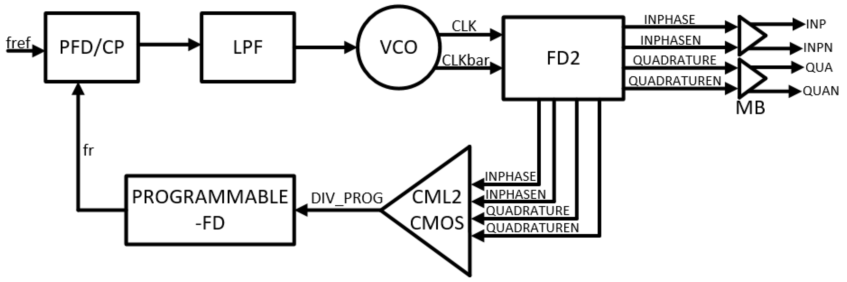
There are different types of SEEs, which are classified depending on the effects they can produce on the circuits [2]. This paper focuses on single event transient (SET) and single event upset (SEU). SETs occur when a particle impacts near or through a PN junction creating a transient pulse [4]. This temporary voltage or current disturbance at a circuit node produces amplitude variations and phase shifts that worsen the signal-to-noise ratio and could cause a change in the circuit state. SEUs occur when a particle passes through a sensitive node of a storage element, such as a flip-flop, causing changes in the stored content [5]. SEUs are especially harmful in frequency synthesizers. As shown in Figure 1, they are based on frequency dividers and a change in the state of one of the flip-flops results in a count error, changing the output frequency [6].
In [5,6,7,8], the effects of space radiation on a phase-locked loop (PLL) and frequency synthesizer were studied, but no RHBD techniques were presented. In [9], a comparison of the effect of radiation on an LC oscillator and a ring oscillator within a PLL was done. It was observed that LC oscillators are more vulnerable than ring oscillators, but no RHBD technique was implemented.
Zhang et al. [10] proposed a RHBD technique to enhance the radiation tolerance of an LC tank oscillator. This technique consists of adding a coupled capacitor to accelerate the current pulse discharge in the bias transistor. In addition, two AC coupled capacitors are added between the varactors and the LC tank to block the voltage distortion.
In [11], a set-hardened-by-design charge pump (SET-HBD-CP) to improve SET tolerance of the CP in a PLL was proposed. The SET-HBD-CP approach consists of a basic CP, a reference circuit and a radiation-hardened circuit. When an impact occurs, the radiation-hardened circuit will work and provide the compensation current so as to improve the additional charge of the struck node. Improved results for the recovery time, phase shift and disturbance in the PLL were obtained. For example, when a particle impacts with a linear energy transfer (LET) of 1 pC/m on the output node of the charge pump, the maximum recovery time, voltage perturbation and phase shift improvement are 72%, 93.7% and 91.8%, respectively.
In [12], an SEU tolerant frequency divider was proposed. This RHBD approach detects the SEU-induced errors via counting the number of rising clock edges and corrects the errors via resetting the faulty frequency divider to a proper state.
In [13], several RHBD techniques for a low-jitter PLL in 130 nm partially depleted-silicon-on -insulator (PD-SOI) process were presented. For the CP, a stacked RHBD technique based on low mismatch current was implemented. The RHBD voltage controlled oscillator (VCO) technique was based on a current compensation scheme and a triple modular redundancy (TMR) technique. In addition, the TMR technique was also implemented in the programmable frequency divider (Programmable-FD) to make the circuit robust to radiation.
In this paper, a thorough study of SETs and SEUs effects in a frequency synthesizer is presented. Section 2 describes the design and operation of the frequency synthesizer that will serve as the basis for our study and, in Section 3, the radiation analysis is performed. On the basis of this study, Section 4 describes the RHBD techniques that are implemented to increase the robustness of the most vulnerable circuits. Finally, some conclusions are drawn in Section 5.
2. Architecture of the Frequency Synthesizer
The frequency synthesizer was designed to fulfill the specifications of the IEEE 802.15.4 standard when a zero-IF receiver architecture is used. In this case, a frequency range from 2405 MHz to 2480 MHz has to be covered with a channel spacing of 5 MHz and the phase noise has to be −102 dBc/Hz @ 3.5 MHz [14].
2.1. Phase-Frequency Detector (PFD) and Charge Pump (CP)
A conventional PFD was designed. This circuit employs a sequential logic and responds to the rising edges of the two inputs [15]. Typically, the PFD outputs are connected to a CP that consists of two switched current sources that charge or discharge the loop filter according to two logical signal inputs [16].
2.2. Low Pass Filter (LPF)
The loop filter is a passive three-pole filter. This comprises a second order filter section and a RC section, providing an extra pole to assist the attenuation of the side-bands at multiples of the comparison frequency that may appear [17].
2.3. Voltage Controlled Oscillator (VCO)
The VCO was implemented as an LC oscillator in CMOS configuration where all the tank components are integrated on-chip. This architecture provides higher transconductance for a given bias current, which results in faster switching and low sensitivity to ion impacts [18].
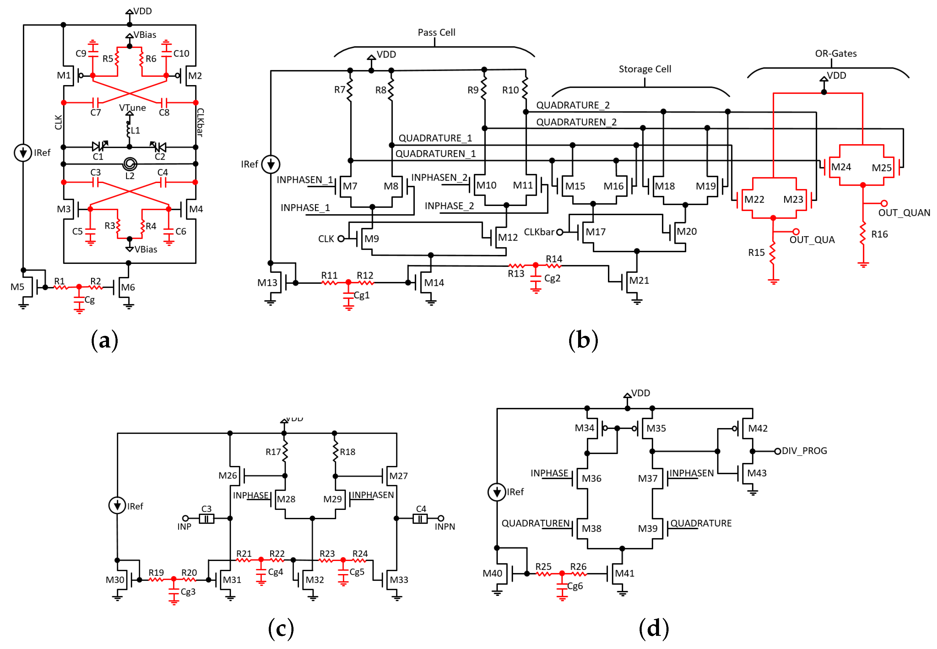
Figure 2a shows the schematic of the VCO. The core is composed by the cross-coupled pair transistors (M1–M4) to obtain the negative resistance and the LC tank. To control the oscillation frequency of the VCO, a voltage (VTune) is applied to the MOS varactors (C1 and C2). The output signals are CLK and CLKbar and the current source (IRef) and the transistors M5 and M6 are used to bias the oscillator.
2.4. Frequency Divider by Two (FD2)
The VCO output is connected to the FD2 in order to generate the in-phase (I) and quadrature (Q) signals necessary for the O-QPSK modulation [14]. The CML (current-mode logic) configuration is chosen to obtain the I-Q signals.
Figure 2b shows the schematic of the FD2 with the CML structure, which consists of two D flip-flops in master–slave configuration. It is composed by a sampling stage (M7, M8, M15 and M16), and a hold stage (M10, M11, M18 and M19) whose objective is to maintain the voltage at the output node. The current source (IRef); the transistors M13, M14 and M21; and the pull-up resistances are used to bias the circuit. The control signals, CLK and CLKbar, come from the VCO output. The differential output signals are in-phase signals (INPHASE and INPHASEN) and quadrature signals (QUADRATURE and QUADRATUREN).
2.5. Mixer Buffer (MB) and CML to CMOS Converter (CML2CMOS Converter)
The MB for the in-phase signal is shown in Figure 2c. The same schematic is used for the quadrature signal. The MB has a differential input stage and a source follower output stage.
To drive the Programmable-FD, a CML2CMOS converter in a D2SE (Differential to Single-Ended) configuration is used [19]. The schematic of this circuit is shown in Figure 2d. The control signals of the differential stages are in-phase signals (INPHASE and INPHASEN). The quadrature signals (QUADRATURE and QUADRATUREN) are added to avoid overloading the output. The current source IRef and transistors M36 and M37 are used to bias the circuit. At the output, an inverter stage formed by M38 and M39 is used to obtain a digital signal to drive the Programmable-FD.
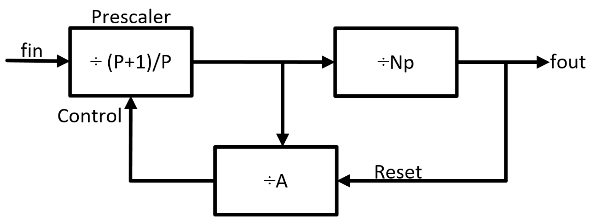
2.6. Programmable Frequency Divider (Programmable-FD)
Figure 3 shows a block diagram of the Programmable-FD. It is a conventional dual-modulus frequency divider composed by a dual modulus prescaler (P/P + 1), and two programmable counters (Np and A). The prescaler divides by 2/3 the output of the CML2CMOS converter, and Np and A divide by 256 and 8, respectively.
3. SET and SEU Analysis in the Frequency Synthesizer
3.1. Impacts Modeling
In CMOS devices, the most affected areas by an ion impact are the reverse bias junctions. This corresponds to the n-p and p-n junctions between the drain and substrate in NMOS and PMOS transistors, respectively [4]. The effect of an ion impact can be modeled by a current pulse connected to the drain of the transistor. This current pulse is generally described as a double exponential with the following expression [20,21]:
where Q is the collected charge, while tf and tr are the fall and rise times, respectively. Typically, tf and tr are of the order of hundreds of picoseconds and tens of picoseconds, respectively [22,23], and Q goes from several hundreds of fC to about 1200 fC. Table 1 shows the values used in this study, which are the expected numbers for a 180 nm CMOS process [22].
The LET is defined as the energy that loses the particle until it reaches rest. It can be calculated by the following expression:
where e is the electron charge, is the silicon density, d is the sensitive depth of the charge collection and the constant 3.6 corresponds to the energy required in eV to create an electron–hole pair in silicon [20,22]. Figure 4 shows the time domain waveforms of the current pulses. An impact of a charged particle in the n-p and p-n junctions between the drain and substrate in NMOS and PMOS transistors generates electron–hole pairs, which results in a current peak. This current slowly decays as these extra electron–hole pairs recombine. Therefore, the width of the pulse is strictly related with the number of electron–hole pairs generated and how fast they recombine [24].
3.2. SET and SEU Analysis
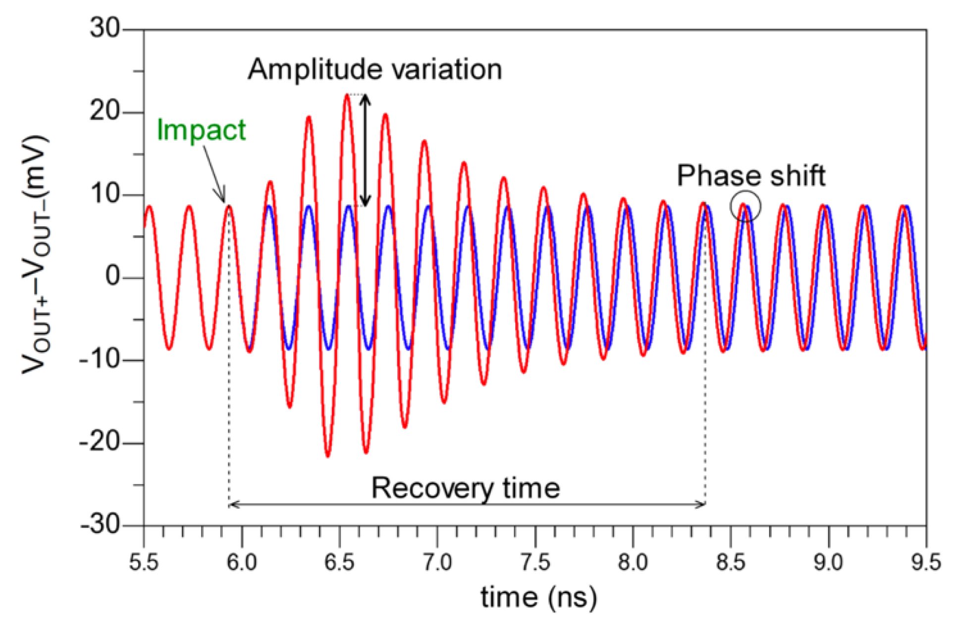
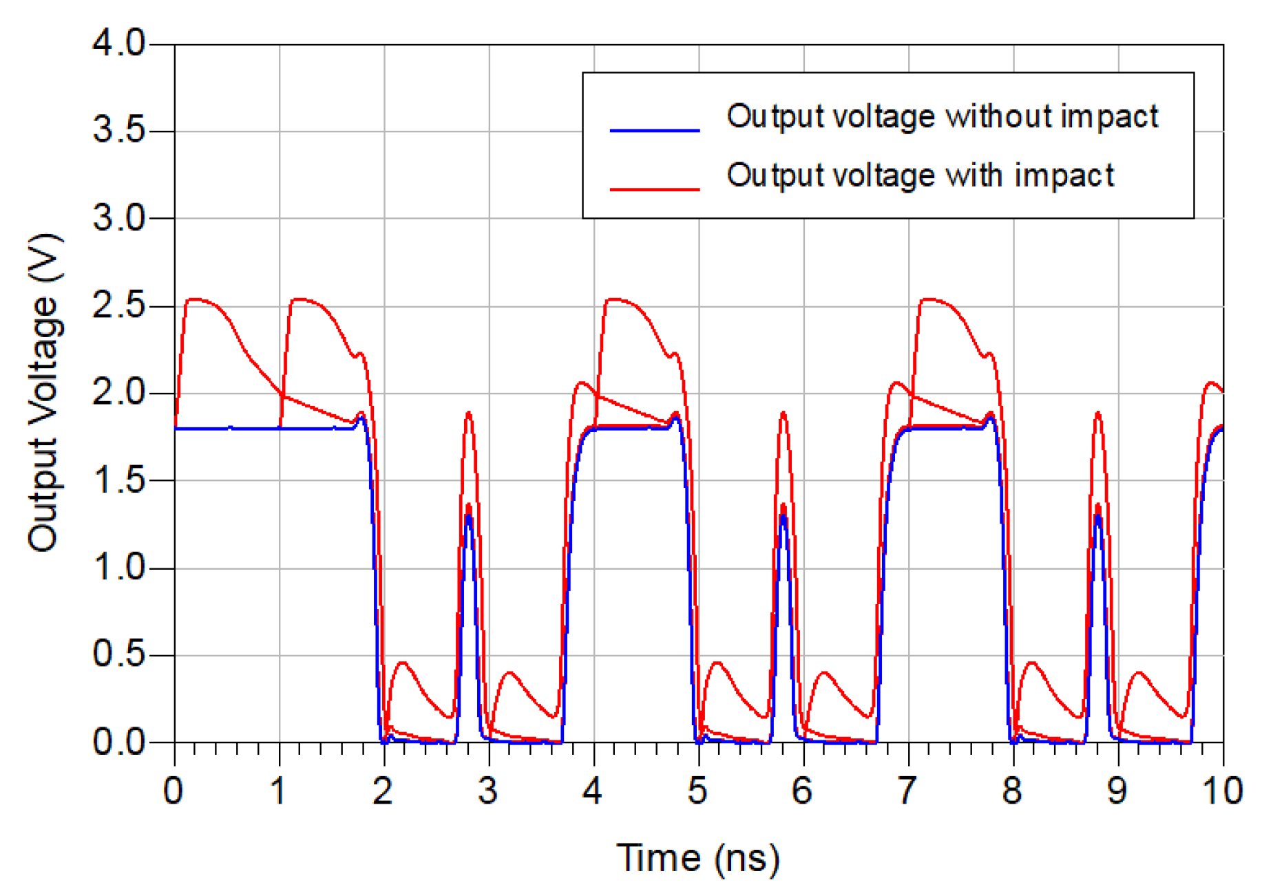
To perform the analysis of the radiation effects on every transistor of the frequency synthesizer, a current pulse was connected to its drain resulting in an amplitude variation and a phase shift of the output signal. Figure 5 compares the output signal for the cases when there is an impact (red) and when there is no impact (blue). The recovery time is defined as the time it takes the signal amplitude to return to its value without impact with an error of less than 5%. This was done for all transistors of the synthesizer. It is important to note that, since the width of the pulses covered several periods of a 5 GHz signal, there was no appreciable difference between impacting at the peaks or at the zero crossings of the signals [25].
Low frequency circuits such as the PFD, the CP and the LPF were practically unaffected by the current pulses since their operating frequency is 2.5 MHz. This means that the period of the signal was 0.4 s, which was at least one order of magnitude bigger than the pulse widths considered in this study (in the order of a few nanoseconds). For the same reason, high frequency circuits such as the VCO, the FD2, the MB, the CML2CMOS converter and the Programmable-FD were more affected. Figure 2 shows the schematics of those circuits with the current pulses, represented as rays, connected to the drain of the transistors.
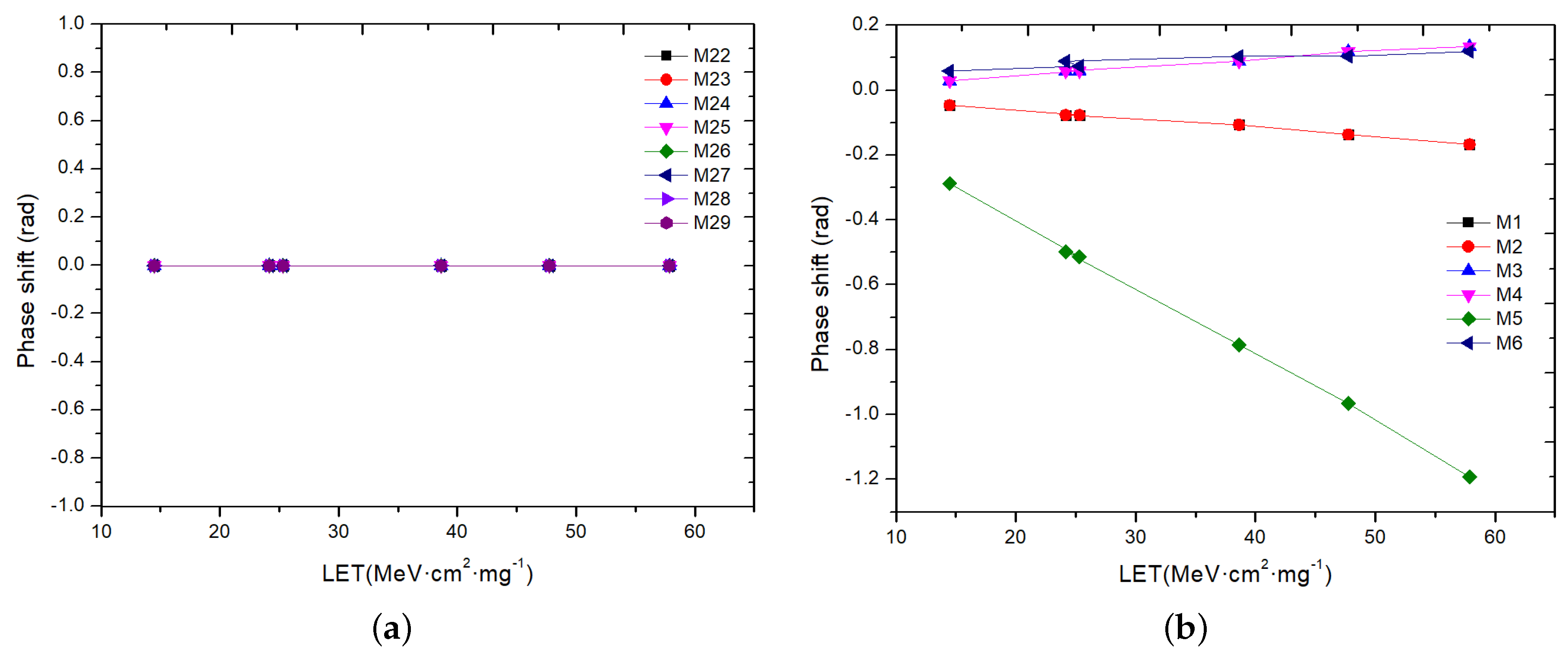
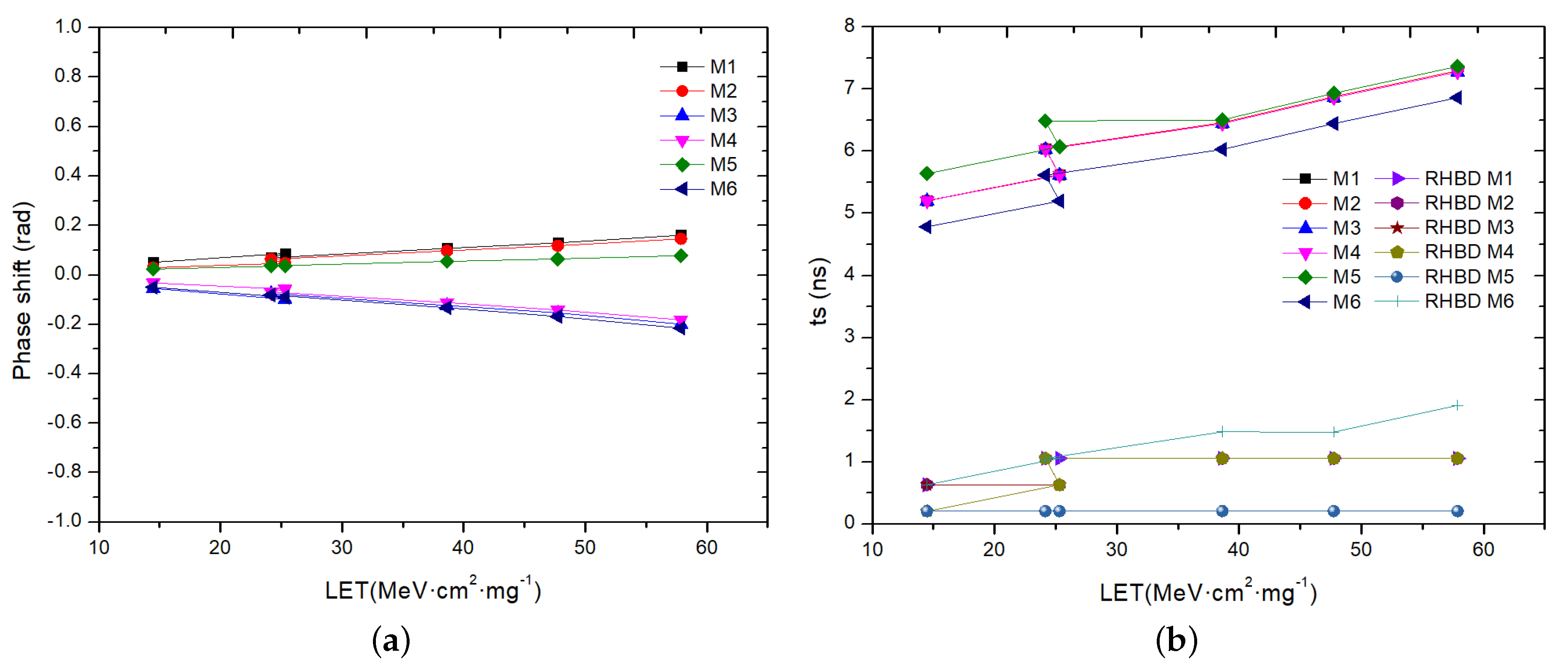
Figure 6 shows the phase shift of one of the frequency synthesizer outputs (INP) due to impacts on the transistors of the VCO, the CML2CMOS converter, the FD2 and the MB. The other frequency synthesizer outputs had a similar behavior. As shown in Figure 6, there were circuits that were very vulnerable to impacts and others that were practically invulnerable. For example, impacts on the MB were not affected since the phase changes were practically negligible (see Figure 6a). However, other circuits such as the VCO and the CML2CMOS converter were more affected by the impacts. In the case of the VCO, the current mirror transistor M5 was the most sensitive component since at high energy a high phase shift was produced [25]. This can be seen in Figure 6b. Figure 6c shows that, in the CML2CMOS converter, the most vulnerable transistor was M35 since at certain LET values the phase shift was also large. It should be taken into account that a 180 phase shift is equivalent to a SEU that can be propagated to other circuits.
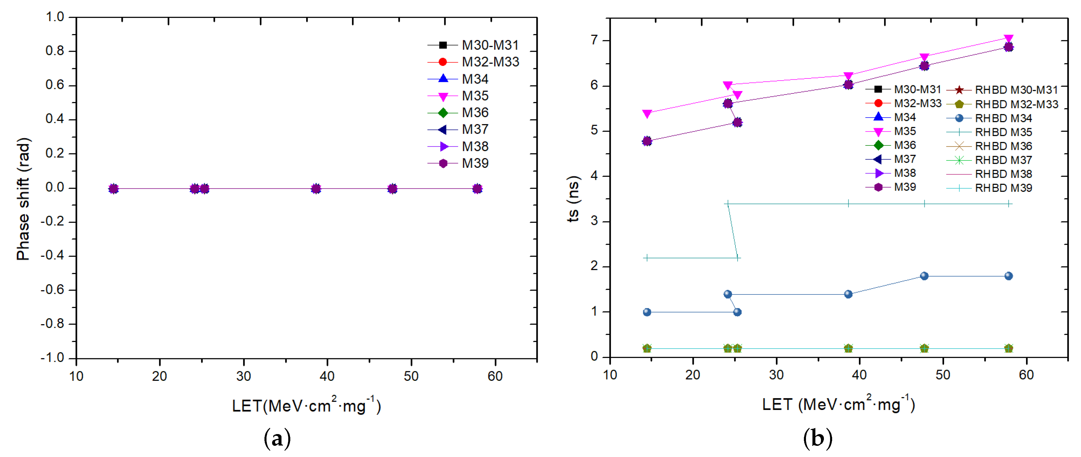
The FD2 was extremely sensitive to impacts. Figure 6d shows that an ion impact on any transistor produced a 180 phase shift for different LET values. As stated above, this produced a SEU at the divider output that can be propagated to other parts of the circuit, causing an incorrect output.
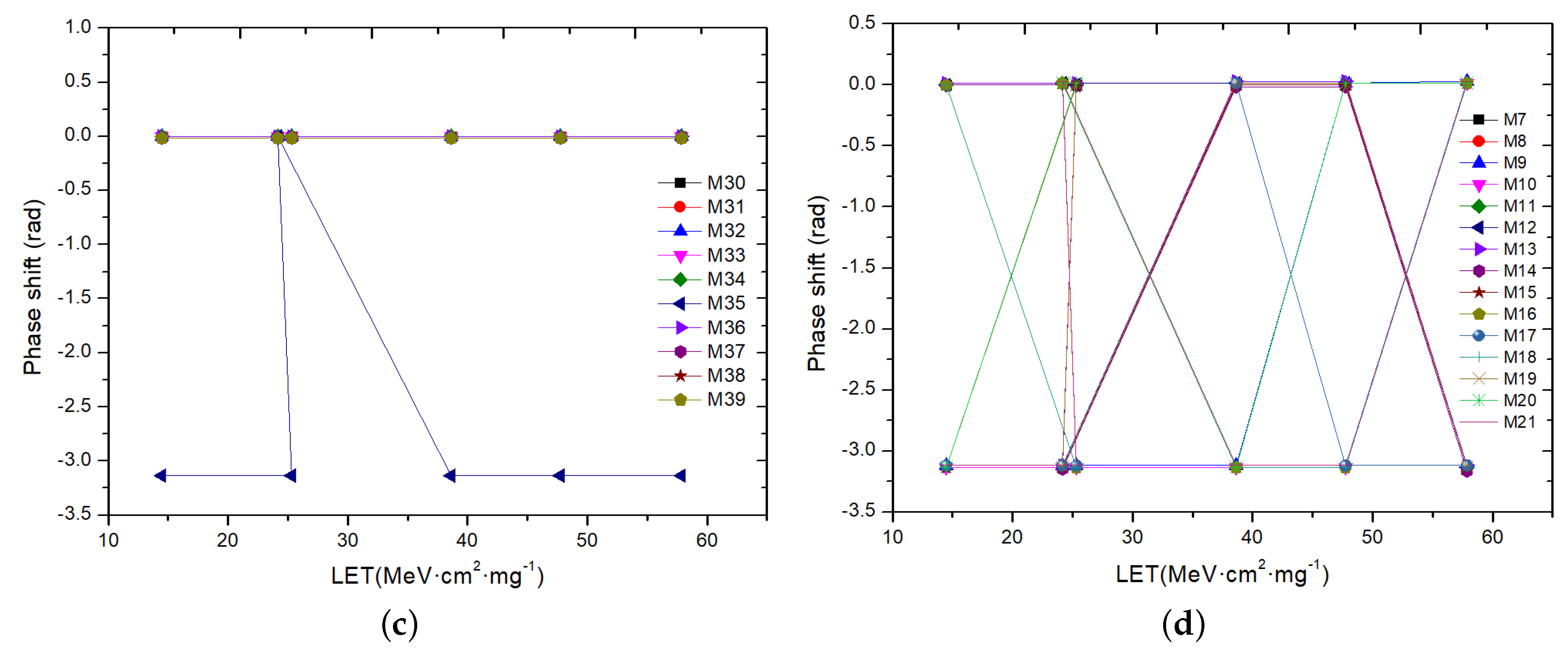
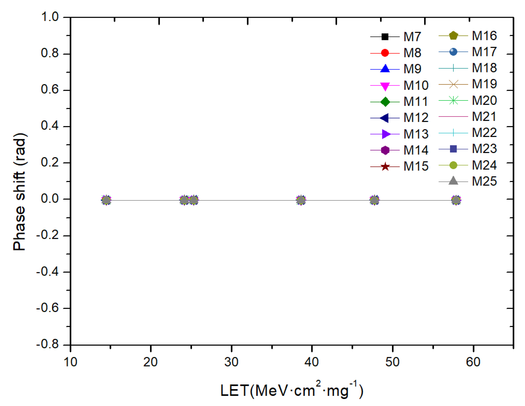
Figure 7 shows the output of the Programmable-FD when impacts were applied each nanosecond in the prescaler. As seen in the figure, amplitude variations were observed at the output of this circuit but no changes in the state of the divider was observed.
4. RHBD Design
In this section, the most sensitive circuits are redesigned using RHBD techniques.
4.1. VCO
The simulation results shown in Section 3 indicate that the VCO was considerably more sensitive to strikes at the biasing network of the circuit (transistors M5 and M6) [26]. Therefore, the RHBD technique proposed in this paper is focused on this node. This mitigation technique should improve the SET performance of the VCO without affecting its RF performance.
Resistor–capacitor (RC) filtering was implemented to achieve a RHBD VCO. Figure 8a shows the schematic of the redesigned VCO. Two resistors, R1 and R2 (both with a value of 4.7 k), and the capacitor Cg (1 pF) were added to increase the time constant ( = RC) on the gates of transistors M5 and M6, resulting in a much lower output voltage deviation due to the SET. A drawback of this technique is that the phase noise of the oscillator no longer met the standard specification (−102 dBc/Hz @3.5 MHz) due to the thermal noise of resistors R1 and R2. To improve the phase noise, a common technique used is to increase the amplitude of oscillation [27]. To do this, a capacitive divider consisting of four capacitors and two resistors were added to the N and P cross-coupled pair transistors. This divider reduced the voltage in the drains of M1–M4, thus increasing the maximum output swing at the drains of these transistors.
Figure 9 shows the phase noise of the VCO before and after RHBD design. As seen in the figure, the VCO met the specifications of the standard with a phase noise that was even better than the original design.
4.2. FD2
Two RHBD circuit-redundancy techniques were employed in the FD2: Dual interlocked storage cell (DICE) [28] and gated feedback cell (GFC) [29]. In both techniques, the layout should be carefully implemented and the critical nodes should be spatially separated.
The FD2 schematic shown in Figure 2b is based on a standard master–slave D-flip-flop and suffers from an increased vulnerability to SEU due to cross-coupling at the transistor-level required for the storage cell functionality. Local redundancy mitigates its SEU sensitivity with only a moderate increase in power consumption and circuit complexity. Figure 8b shows the schematic of the master stage of the D-flip flop with local redundancy. The gate and the drain of the transistors in the storage cell are not connected to the same differential pair in the pass cell, thus achieving effective decoupling of the gate and drain terminals of the transistors in the storage cell and, as a consequence, reducing its SEU sensitivity. This technique is commonly referred as dual interlocked storage cell.
The other technique, called gated feedback cell, is also shown in Figure 8b applied to a single latch of the divider by two. The latch outputs are connected to a pair of OR gates that hold the circuit stable when an impact occurs, since the output of a two-input OR gate changes state only when both inputs change their state from high to low or from low to high [29]. The OR operation comprises a pair of source followers (M22–M25) that helps to transmit the correct logic value to the storage cell inputs even when one of the OR gate inputs is in error due to an ion strike. Resistances R15 and R16, each of 55 k, were also included.
The OR-gate-based feedback to the storage cell inputs, in addition to local redundancy, is expected to offer a high SEU immunity. However, the technique of increasing the time constant in the bias circuits was also used. Resistors R11–R14 (each of 4.7 k) and capacitors Cg1 and Cg2 (1 pF each) were added to increase the time constant ( = RC) in the gate terminal of transistors M13, M14 and M21, which are part of the bias circuit network.
4.3. CML2CMOS Converter and MB
Similar to the previous circuits, the most sensitive nodes of the CML2CMOS converter and the MB were those of the biasing networks. The same RHBD technique based on increasing the time constant was used. The resistances and capacitors included had the same values as for the VCO and the FD2, 4.7 k and 1 pF, respectively. Figure 8c,d shows the RHBD schematics.
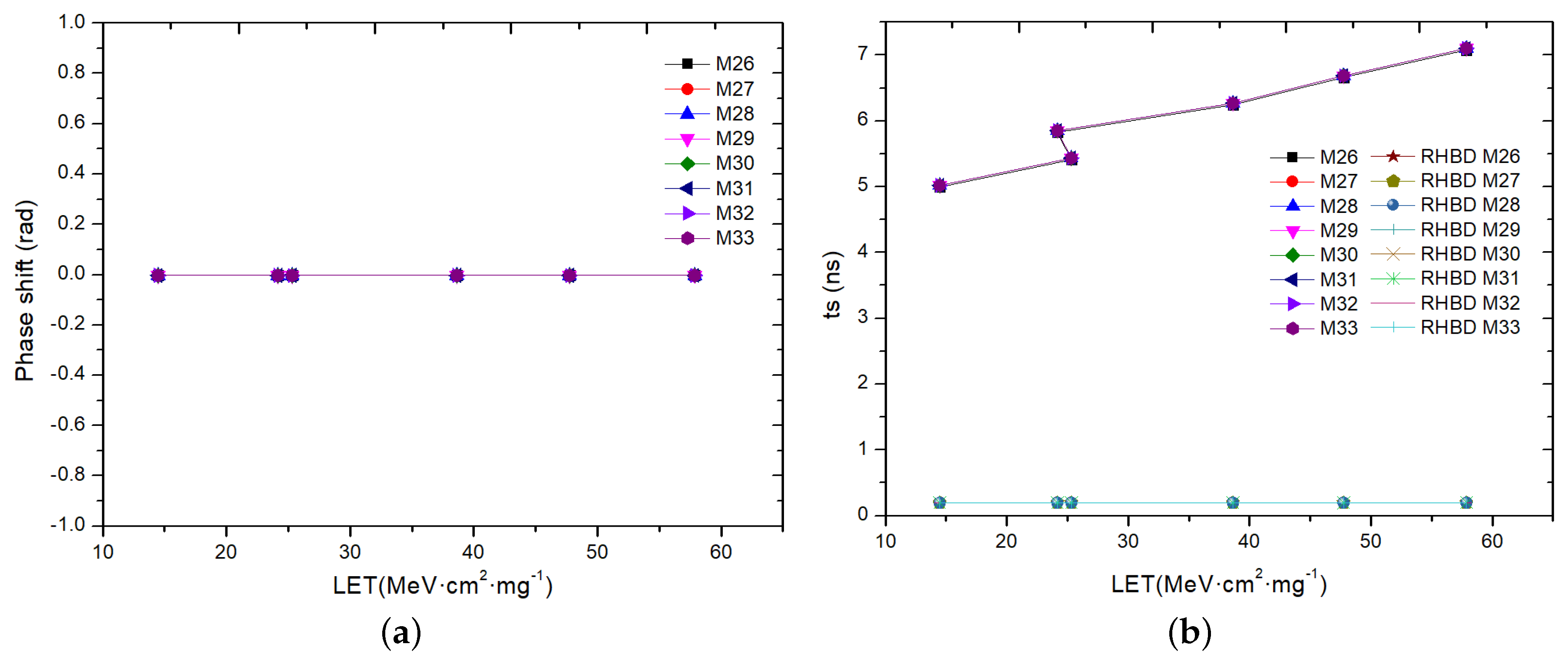
Figure 13a shows that the phase shift of the CML2CMOS converter was almost zero for all transistors, disappearing the SEU in this circuit. Figure 13b shows a comparison of the recovery time before and after the RHBD design. As seen in the figure, after applying the RHBD technique, the recovery time was reduced by 3 ns, obtaining an overall improvement of 78.83%.
As mentioned in Section 3, impacts in the MB did not produce 180 phase shifts at the output. As shown in Figure 14a, the results are very similar before (see Figure 6a) and after RHBD design. Figure 14b shows the recovery time of the INP output before and after RHBD design. The recovery time was almost zero, thus an overall improvement of 77.9% was obtained for this circuit.
5. Conclusions
This paper presents a comprehensive study of the effects of SETs and SEUs on a frequency synthesizer for the IEEE 802.15.4 standard. The blocks that work at low frequencies, such as the PFD, the CP and the LPF, are not affected by ion impacts. However, high frequency circuits such as the Programmable-FD, the VCO, the FD2, the CML2CMOS converter and the MB are more vulnerable. In the Programmable-FD, amplitude variations of the output signal occur, but there is no change in the state of the divider, thus no RHBD techniques were applied. This is not the case in the rest of the high frequency circuits, thus RHBD techniques were implemented on them. The VCO’s radiation tolerance was improved using resistor–capacitor (RC) filtering and a capacitive divider was introduced to improve the degraded phase noise. The combination of both techniques resulted in a substantial improvement on the VCO performance, reducing by approximately 50% the output phase displacement and by 81% the recovery time. RC filtering of the bias circuits was also used in the FD2, the CML2CMOS converter and the MB. In addition, local circuit-redundancy hardening techniques were employed in the flip flops of the FD2. The proposed modifications make the frequency synthesizer more robust against radiation: SEU effects were fully mitigated and the SETs were reduced considerably. Furthermore, the power consumption of the PLL was increased from 18.5 mW to 21.2 mW due to the local circuit-redundancy technique.
Author Contributions
All authors contributed to the study of the radiation in the frequency synthesizer and the writing process of the paper.
Funding
This research was funded by the Spanish Ministry of Economy and Competitiveness grant number TEC2015- 71072-C03-01; by the Spanish Ministry of Science, Innovation and Universities grant number RTI2018- 099189-B-C22; by the Canary Agency for Research, Innovation and Information Society (ACIISI) of the Canary Islands Government grant number ProID2017010067; and the “Programa Predoctoral de Formación del Personal Investigador” of the ULPGC.
Acknowledgments
The authors would like to thank Raquel León-Martín for her contributions on this paper.
Conflicts of Interest
The authors declare no conflict of interest.
Abbreviations
The following abbreviations are used in this manuscript:
| CML | Current-Mode Logic |
| CML2CMOS converter | CML to CMOS converter |
| CMOS | Complementary Metal-Oxide-Semiconductor |
| CP | Charge Pump |
| DICE | Dual Interlocked Storage Cell |
| D2SE | Differential to Single-Ended |
| FD2 | Frequency Divider by 2 |
| GFC | Gated Feedback Cell |
| IEEE | The Institute of Electrical and Electronics Engineers |
| LET | Linear Energy Transfer |
| LPF | Low Pass Filter |
| MB | Mixer Buffer |
| O-QPSK | Offset Quadrature Phase Shift Keying |
| PD-SOI | Partially Depleted-Silicon-on-Insulator |
| PFD | Phase Frequency Detector |
| Programmable-FD | Programmable Frequency Divider |
| PLL | Phase-Locked Loop |
| RC | Resistor–Capacitor |
| RF | Radio Frequency |
| RHBD | Radiation Hardening-By-Design |
| SEE | Single Event Effect |
| SET | Single Event Transient |
| SET-HBD-CP | SET-Hardened-By-Design Charge Pump |
| SEU | Single Event Upset |
| TMR | Triple Modular Redundancy |
| VCO | Voltage Controlled Oscillator |
| WSN | Wireless Sensor Networks |
References
- Bagatin, M.; Gerardin, S. Ionizing Radiation Effects in Electronics: From Memories To Imagers; CRC Press: Boca Raton, FL, USA, 2015; p. 391. [Google Scholar]
- Gaillard, R. Single Event Effects: Mechanisms and Classification. In Soft Errors in Modern Electronic Systems. Frontiers in Electronic Testing; Springer: Boston, MA, USA, 2011; pp. 27–54. [Google Scholar] [CrossRef]
- Kerns, S.E.; Shafer, B.D. The Design of Radiation-Hardened ICS for Space: A Compendium of Approaches. Proc. IEEE 1988, 76, 1470–1509. [Google Scholar] [CrossRef]
- Wang, T. Study of Single-Event Transient Effects on Analog Circuits. Ph.D. Thesis, University of Saskatchewan, Saskatoon, SK, Canada, 2011. [Google Scholar]
- Dayaratna, L.; Seehra, S.; Bogorad, A.; Ramos, L. Single event upset characteristics of some digital integrated frequency synthesizers. In Proceedings of the 1999 IEEE Radiation Effects Data Workshop. Workshop Record. Held in conjunction with IEEE Nuclear and Space Radiation Effects Conference (Cat. No.99TH8463), Norfolk, VA, USA, 12–16 June 1999; pp. 46–52. [Google Scholar] [CrossRef]
- Chung, H.H.; Chen, W.; Bakkaloglu, B.; Barnaby, H.J.; Vermeire, B.; Kiaei, S. Analysis of Single Events Effects on Monolithic PLL Frequency Synthesizers. IEEE Trans. Nucl. Sci. 2006, 53, 3539–3543. [Google Scholar] [CrossRef]
- Sotskov, D.I.; Elesin, V.V.; Kuznetsov, A.G.; Nazarova, G.N.; Chukov, G.V.; Boychenko, D.V.; Telets, V.A.; Usachev, N.A. Total Ionizing Dose Effects in Phase-Locked Loop ICs and Frequency Synthesizers. In Proceedings of the 2015 15th European Conference on Radiation and Its Effects on Components and Systems (RADECS), Moscow, Russia, 14–18 September 2015; pp. 1–3. [Google Scholar] [CrossRef]
- Chen, Z.; Ding, D.; Dong, Y.; Shan, Y.; Zhou, S.; Hu, Y.; Zheng, Y.; Peng, C.; Chen, R. Study of Total-Ionizing-Dose Effects on a Single-Event-Hardened Phase-Locked Loop. IEEE Trans. Nucl. Sci. 2018, 65, 997–1004. [Google Scholar] [CrossRef]
- Prinzie, J.; Christiansen, J.; Moreira, P.; Steyaert, M.; Leroux, P. Comparison of a 65 nm CMOS ring- and lc-oscillator based PLL in terms of TID and SEU sensitivity. IEEE Trans. Nucl. Sci. 2017, 64, 245–252. [Google Scholar] [CrossRef]
- Zhang, Z.; Chen, L.; Djahanshahi, H. A Hardened-By-Design Technique for LC-Tank Voltage Controlled Oscillator. In Proceedings of the 2018 IEEE Canadian Conference on Electrical & Computer Engineering (CCECE), Quebec City, QC, Canada, 13–16 May 2018; pp. 1–4. [Google Scholar] [CrossRef]
- Zhou, Q.; Zhang, C.; Tan, J.; Zhu, L.; Wang, L.; Luo, W. A SET-hardened phase-locked loop. In Proceedings of the 2017 IEEE 3rd Information Technology and Mechatronics Engineering Conference (ITOEC), Chongqing, China, 3–5 October 2017; pp. 196–199. [Google Scholar] [CrossRef]
- Li, N.; She, X. Single event transient tolerant frequency divider. IET Comput. Digit. Tech. 2014, 8, 140–147. [Google Scholar] [CrossRef]
- Chen, Z.; Lin, M.; Ding, D.; Zheng, Y.; Sang, Z.; Zou, S. Analysis of Single-Event Effects in a Radiation-Hardened Low-Jitter PLL Under Heavy Ion and Pulsed Laser Irradiation. IEEE Trans. Nucl. Sci. 2017, 64, 106–112. [Google Scholar] [CrossRef]
- Standards Committee of the IEEE Computer Society. IEEE Standard for Local and Metropolitan Area Networks—Part 15.4: Low-Rate Wireless Personal Area Networks (WPANs); IEEE Std 802.15.4-2011; Standards Committee of the IEEE Computer Society: New York, NY, USA, 2006. [Google Scholar]
- Weste, N.H.E.; Harris, D.M. CMOS VLSI Design: A Circuits and Systems Perspective; Addison Wesley: Boston, MA, USA, 2011; p. 838. [Google Scholar]
- Razavi, B. Design of Analog CMOS Integrated Circuits; McGraw-Hill: New York, NY, USA, 2001; p. 684. [Google Scholar]
- Fujitsu Microelectronics America Inc. Super PLL Application Guide: Integer PLL Loop Filter Design; Fujitsu Microelectronics America Inc.: San Jose, CA, USA, 2002; pp. 22–24. [Google Scholar]
- Hajimiri, A.; Lee, T. Design issues in CMOS differential LC oscillators. IEEE J. Solid-State Circuits 1999, 34, 717–724. [Google Scholar] [CrossRef] [Green Version]
- Senjaliya, C.; Neelakantan, U. 180 nm CMOS process based L-band CML to CMOS converter. IJARIIE 2018, 4, 3697–3700. [Google Scholar]
- Portela-Garcia, M.; Lopez-Ongil, C.; Garcia-Valderas, M.; Entrena, L.; Thys, G.; Redant, S. Assessing SET sensitivity of a PLL. In Proceedings of the Design of Circuits and Integrated Systems, Madrid, Spain, 26–28 November 2014; pp. 1–6. [Google Scholar] [CrossRef]
- Garg, R.; Khatri, S.P. Analysis and Design of Resilient VLSI Circuits. Ph.D. Thesis, Texas A&M University, College Station, TX, USA, 2010. [Google Scholar] [CrossRef] [Green Version]
- Lochner, S.; Deppe, H. Radiation studies on the UMC 180 nm CMOS process at GSI. In Proceedings of the 2009 European Conference on Radiation and Its Effects on Components and Systems, Bruges, Belgium, 14–18 September 2009; pp. 614–616. [Google Scholar] [CrossRef]
- Eaton, P.; Benedetto, J.; Mavis, D.; Avery, K.; Sibley, M.; Gadlage, M.; Turflinger, T. Single event transient pulsewidth measurements using a variable temporal latch technique. IEEE Trans. Nucl. Sci. 2004, 51, 3365–3368. [Google Scholar] [CrossRef]
- Mateos-Angulo, S.; Rodríguez, R.; del Pino, J.; González, B.; Khemchandani, S.L. Single event effects analysis and charge collection mechanisms on AlGaN/GaN HEMTs. Semicond. Sci. Technol. 2019, 34, 035029. [Google Scholar] [CrossRef]
- González Ramírez, D.; Lalchand Khemchandani, S.; del Pino, J.; Mayor-Duarte, D.; San Miguel-Montesdeoca, M.; Mateos-Angulo, S. Single event transients mitigation techniques for CMOS integrated VCOs. Microelectron. J. 2018, 73, 37–42. [Google Scholar] [CrossRef]
- Mateos-Angulo, S.; San-Miguel-Montesdeoca, M.; Mayor-Duarte, D.; Khemchandani, S.L.; del Pino, J. SET analysis and radiation hardening techniques for CMOS LNA topologies. Semicond. Sci. Technol. 2018, 33, 085010. [Google Scholar] [CrossRef]
- Lalchand Khemchandani, S.; del Pino Suarez, J.; Diaz Ortega, R.; Hernandez, A. A fully integrated single core VCO with a wide tuning range for DVB-H. Microw. Opt. Technol. Lett. 2009, 51, 1338–1343. [Google Scholar] [CrossRef]
- Calin, T.; Nicolaidis, M.; Velazco, R. Upset hardened memory design for submicron CMOS technology. IEEE Trans. Nucl. Sci. 1996, 43, 2874–2878. [Google Scholar] [CrossRef]
- Krithivasan, R.; Marshall, P.W.; Nayeem, M.; Sutton, A.K.; Kuo, W.M.; Haugerud, B.M.; Najafizadeh, L.; Cressler, J.D.; Carts, M.A.; Marshall, C.J.; et al. Application of RHBD Techniques to SEU Hardening of Third-Generation SiGe HBT Logic Circuits. IEEE Trans. Nucl. Sci. 2006, 53, 3400–3407. [Google Scholar] [CrossRef]
Figure 1.
Frequency synthesizer block diagram.

Figure 2.
Schematic of the frequency synthesizer most vulnerable circuits. (a) Voltage controlled oscillator (VCO); (b) Frequency divider by two (FD2); (c) Mixer buffer (MB); (d) Current-mode logic to CMOS (CML2CMOS) converter.
Figure 2.
Schematic of the frequency synthesizer most vulnerable circuits. (a) Voltage controlled oscillator (VCO); (b) Frequency divider by two (FD2); (c) Mixer buffer (MB); (d) Current-mode logic to CMOS (CML2CMOS) converter.

Figure 3.
Programmable frequency divider (Programmable-FD) block diagram.

Figure 4.
Current pulse shapes used for single event transient (SET) prediction.
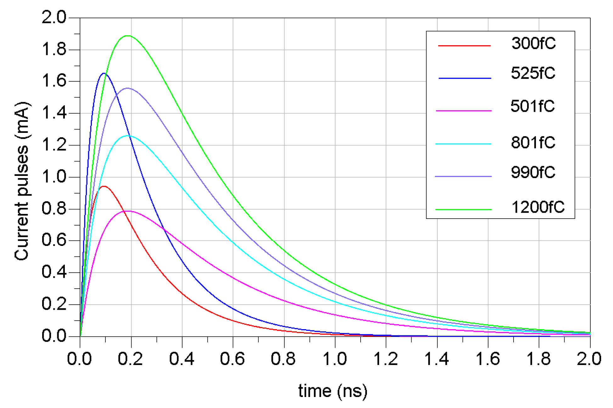
Figure 5.
The blue signal is the output without an impact on any transistor and the red signal is the signal when there is an impact on a transistor.
Figure 5.
The blue signal is the output without an impact on any transistor and the red signal is the signal when there is an impact on a transistor.

Figure 6.
INP output phase shift due to impacts on the transistors. (a) MB; (b) VCO; (c) CML2CMOS converter; (d) FD2.
Figure 6.
INP output phase shift due to impacts on the transistors. (a) MB; (b) VCO; (c) CML2CMOS converter; (d) FD2.


Figure 7.
The blue signal is the output of the Programmable-FD without any impact and the red signal is when impacts were applied each nanosecond.
Figure 7.
The blue signal is the output of the Programmable-FD without any impact and the red signal is when impacts were applied each nanosecond.

Figure 8.
Radiation hardening-by-design (RHBD) schematics. (a) VCO; (b) Slave stage of the FD2; (c) MB; (d) CML2CMOS converter.
Figure 8.
Radiation hardening-by-design (RHBD) schematics. (a) VCO; (b) Slave stage of the FD2; (c) MB; (d) CML2CMOS converter.

Figure 9.
VCO phase noise.
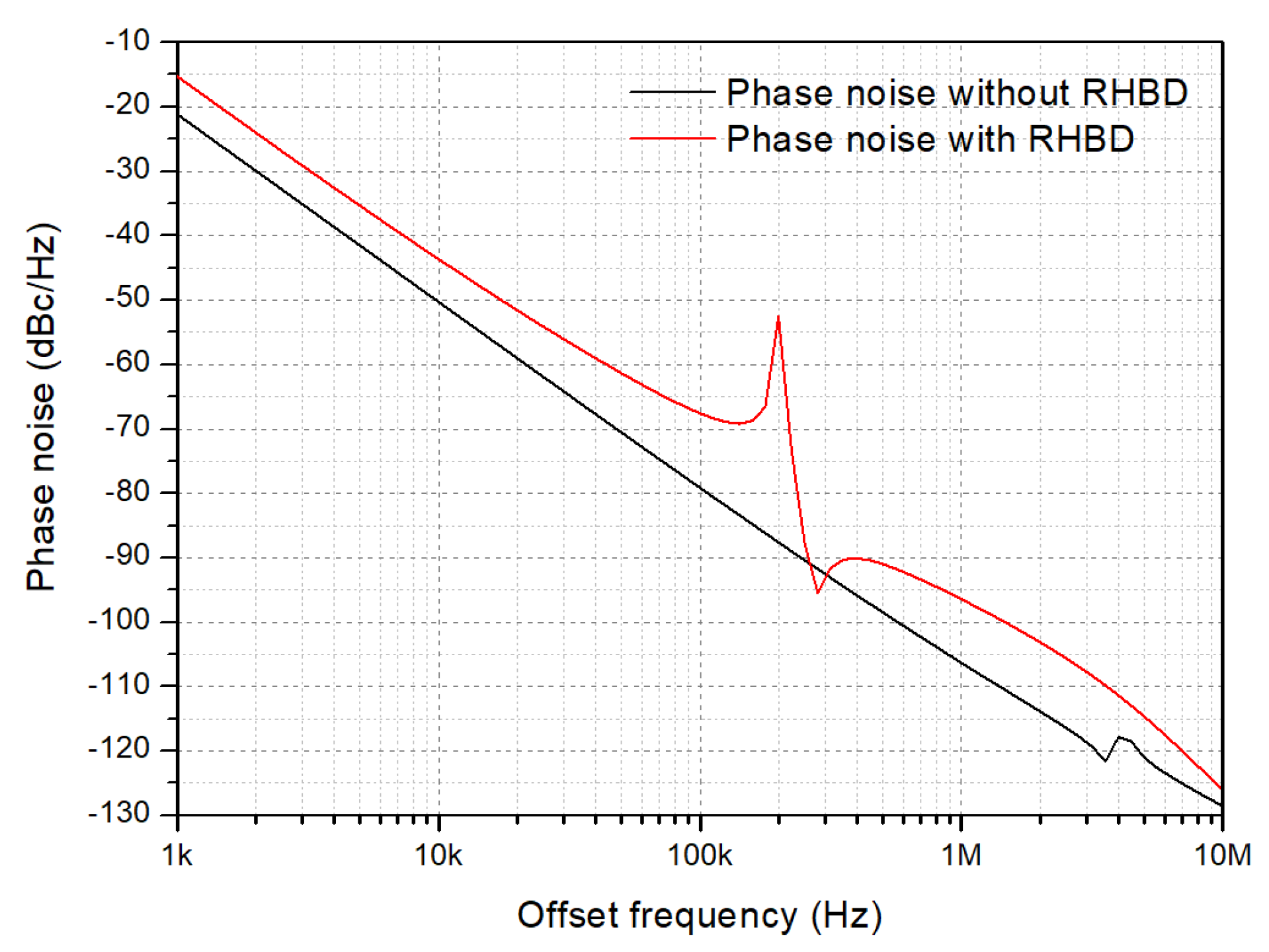
Figure 10.
INP output of the RHBD VCO results. (a) Phase shift; (b) Recovery time.

Figure 11.
INP output of the RHBD FD2 for the phase shift results.

Figure 12.
INP output recovery time of the FD2. (a) Before RHBD; (b) After RHBD.
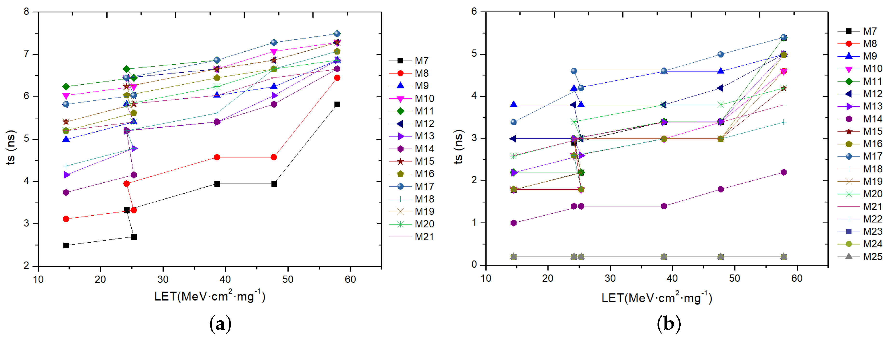
Figure 13.
INP output of the RHBD CML2CMOS converter results. (a) Phase shift; (b) Recovery time.

Figure 14.
INP output of the RHBD MB results. (a) Phase shift; (b) Recovery time.

Table 1.
Current pulses.
| tr (ps) | tf (ps) | Q (fC) | LET, d = 2 m (MeV·cm2·mg−1) |
|---|---|---|---|
| 50 | 200 | 300 | 14.47 |
| 50 | 200 | 525 | 25.31 |
| 100 | 400 | 501 | 24.16 |
| 100 | 400 | 801 | 38.62 |
| 100 | 400 | 990 | 47.74 |
| 100 | 400 | 1200 | 57.86 |
© 2019 by the authors. Licensee MDPI, Basel, Switzerland. This article is an open access article distributed under the terms and conditions of the Creative Commons Attribution (CC BY) license (http://creativecommons.org/licenses/by/4.0/).
Share and Cite
MDPI and ACS Style
Díez-Acereda, V.; L. Khemchandani, S.; del Pino, J.; Mateos-Angulo, S. RHBD Techniques to Mitigate SEU and SET in CMOS Frequency Synthesizers. Electronics 2019, 8, 690. https://doi.org/10.3390/electronics8060690
AMA Style
Díez-Acereda V, L. Khemchandani S, del Pino J, Mateos-Angulo S. RHBD Techniques to Mitigate SEU and SET in CMOS Frequency Synthesizers. Electronics. 2019; 8(6):690. https://doi.org/10.3390/electronics8060690
Chicago/Turabian StyleDíez-Acereda, V., Sunil L. Khemchandani, J. del Pino, and S. Mateos-Angulo. 2019. "RHBD Techniques to Mitigate SEU and SET in CMOS Frequency Synthesizers" Electronics 8, no. 6: 690. https://doi.org/10.3390/electronics8060690
Note that from the first issue of 2016, this journal uses article numbers instead of page numbers. See further details here.