Mechanism of Degradation Rate on the Irradiated Double-Polysilicon Self-Aligned Bipolar Transistor


1
Key Laboratory of Functional Materials and Devices for Special Environments, Xinjiang Technical Institute of Physics and Chemistry, Chinese Academy of Sciences, Urumqi 830011, China
2
University of Chinese Academy of Sciences, Beijing 100049, China
*
Authors to whom correspondence should be addressed.
Electronics 2019, 8(6), 657; https://doi.org/10.3390/electronics8060657
Submission received: 8 April 2019
/
Revised: 26 May 2019
/
Accepted: 27 May 2019
/
Published: 11 June 2019
(This article belongs to the Special Issue Radiation Tolerant Electronics)
Abstract
:The latent enhanced low dose rate sensitivity (ELDRS) effect is observed in the double-polysilicon self-aligned (DPSA) technology PNP bipolar junction transistor (BJT) irradiated with a high and low dose rate gamma ray, which is discussed from the perspective of the three-stage degradation rate of the excess base current. The great degradation rate as a result of the high dose irradiation of the first stage is dominantly ascribed to the positive oxide trap charges accumulated during a short irradiation, and then due to the competition between the recombination of electrons and capture of the hole by the traps. It declined sharply into a degradation rate saturated region of the second stage. However, for the low dose rate, the small increase in the degradation rate in the first stage is caused by the holes escaping from the initial recombination and being transported to the interface to form the interface states. Then, the competition between the steadily increasing interfacial trap charge and the continuously annealed shallow level oxide trap charge leads to the stable increase of degradation under low dose irradiation. Finally, in stage three, the increases of the degradation rates for high and low dose irradiation result from the different amounts of the hydrogen molecules generated by the hole reactive with depassiviated Si suspended bonds, which can interact with the deep level defects and release protons, causing an increase of interfacial trap charges with prolonged irradiation.
1. Introduction
As a state-of-the-art high speed bipolar complementary process, double-polysilicon self-aligned (DPSA) technology has been widely used in high-speed analog integrated circuits. Compared with the traditional bipolar junction transistors (BJTs), DPSA BJTs have a smaller linewidth due to the isolation of local oxidation of silicon (LOCOS) combined with deep trench isolation (DTI). The use of polysilicon emitters can increase the current gain so that the device can achieve vertical scale down without reducing the punch-through voltage of the emitter–collector junction and the loss of the current gain [1,2,3]. The self-aligning structure and DTI can realize the lateral scale down of the device, greatly reduce the area of the device, the circuit, and the corresponding parasitic capacitance, significantly reduce the power consumption delay product of the circuit, and improve the integration level of the bipolar circuit [4,5]. Therefore, the high performance and speed of the analog integrated circuit made by this technology have wide application prospects in space RF(radio frequency)/microwave communication and other extreme environments [6].
The previous total dose irradiation test results in the literature [6,7] have shown that the direct current gain is the most sensitive parameter of the bipolar device under total ionizing dose radiation, and most of the devices and circuits fabricated by bipolar technology suffer from the so-called enhanced low dose rate sensitivity (ELDRS) effect. For decades, most of the total ionizing dose research was focused on the radiation response and the damage mechanism of the traditional bipolar technology; only a few reports were related to the DPSA technology. In 1999, Flamen et.al presented research about the radiation tolerance on quasi-self aligned (QSA) single polysilicon emitter bipolar technology. The experimental results have shown that this bipolar technology is superior to traditional bipolar technology in structure and related function, and that is has a good tolerance of the radiation without adding special manufacturing steps [8]. Graves investigated the radiation and hot-carrier stress response on polysilicon emitter NPN BJTs fabricated in a bipolar-complementary-metal-oxide-semiconductor (BiCMOS) process [9]. More recently, Zhang et al. presented the radiation response on the DPSA NPN BJTs with Si and silicon-on-insulator (SOI) substrate at high and low injection levels [10,11,12,13,14]. However, all of the above research was focused on the preliminary total ionizing dose response on the NPN BJTs. Studies on the dose rate response and the degradation rate of the electrical parameters are still not enough to apply it to real space applications. Thus, in this paper, the dose rate response on the DPSA BJT has been investigated under high and low dose rate gamma ray irradiation and a preliminary analysis of the radiation effect and the damage mechanism is made from the perspective of the degradation rate of the excess base current.
Based on the understanding of the comprehensive research on the radiation damage effect of bipolar transistors, the current gain degradation saturation phenomenon and generation mechanism of the devices at the total dose of 100 krad (Si) were investigated by using a bipolar transistor which is very resistant to total ionizing dose radiation. Section 2 of the paper introduces the devices and the methods used in the experiments. Detailed experimental results are presented in Section 3. Section 4 explains the experimental results and discusses their effects on practical future space applications. Finally, Section 5 concludes the article.
2. Experimental Devices and Methods
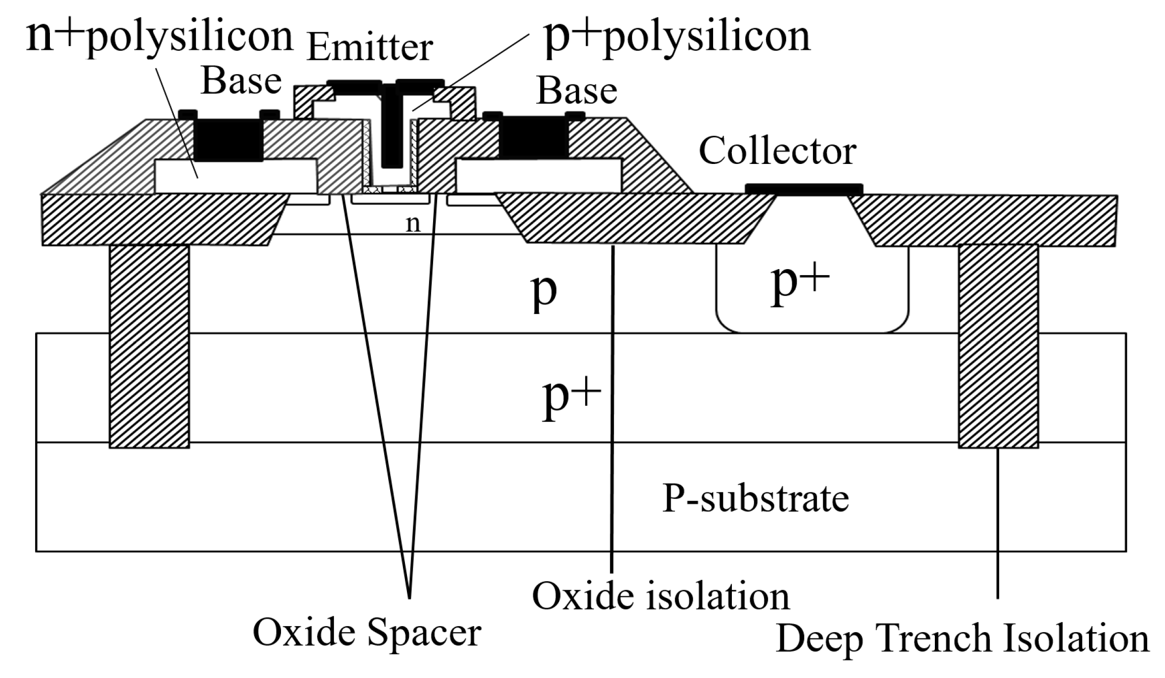
DPSA PNP BJTs studied in this paper adopted a standard bipolar process with the trench isolation technology and the cross-section of the device being depicted in Figure 1. The devices presented here were irradiated with a 60Co gamma ray at the Xinjiang Technical Institute of Physics & Chemistry of Chinese, Academy of Sciences. The devices were exposed at the high and low dose rate of 50 rad (Si)/s and 0.05 rad (Si)/s with a reverse emitter-base bias voltage, which is usually recognized as the worst operation condition [6]. The electrical parameters were measured by the KEITHLEY 4200-SCS semiconductor parameter analyzer by removing the devices under test from the irradiation chamber within 20 minutes before and after the dose accumulated to about 100 krad (Si) at room temperature.
3. Experimental Results
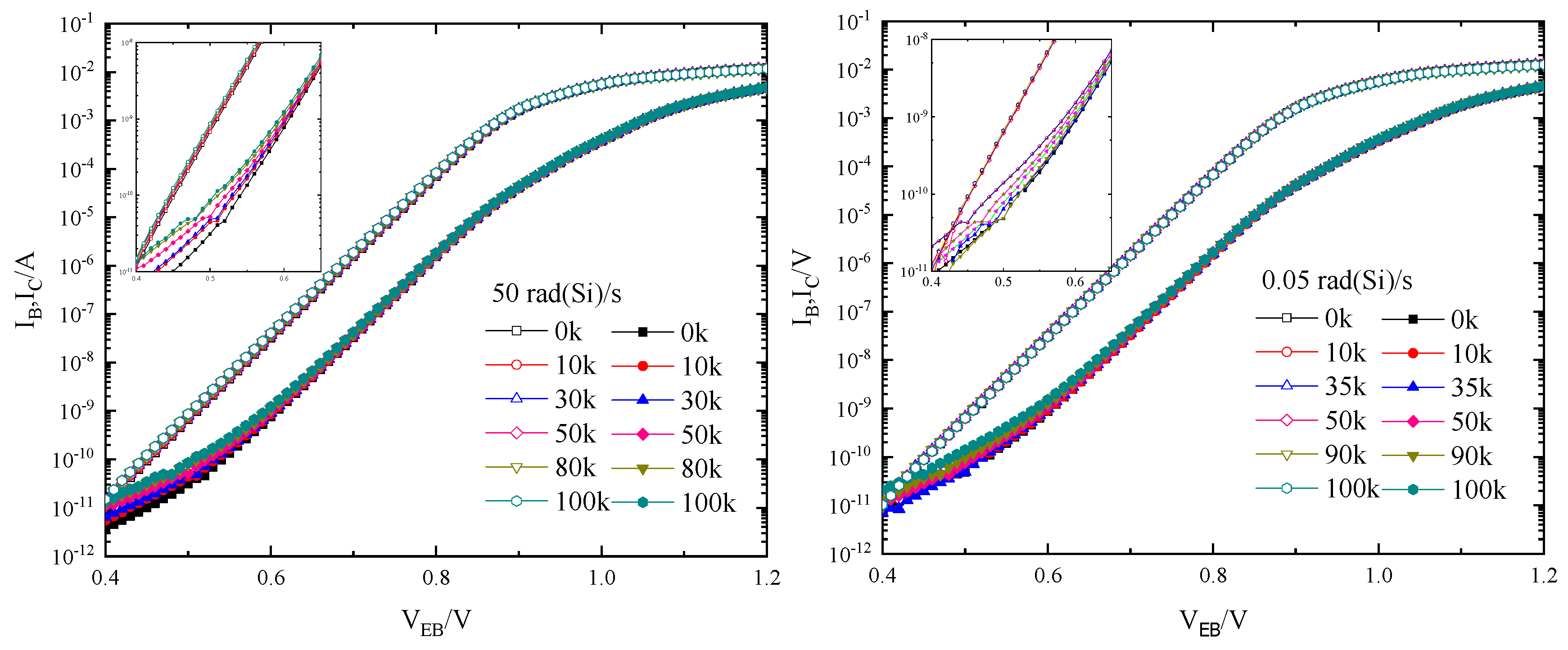
Figure 2 shows the changes in the Gummel curve of the experimental samples with the cumulative total dose before and after irradiation at dose rates of 50 rad (Si)/s and 0.05 rad (Si)/s to 100 krad (Si). As the dose accumulated, the collector current did not change significantly, while the base current increased slightly when biased at the emitter-base voltage lower than VEB = 0.7 V. However, the base current of the irradiated transistor is mainly composed of the initial current and the surface compound current. The oxide trap positive charge and the interface trap charge generated by the irradiation increases the surface recombination rate [7], so the increase of the surface recombination current leads to an increase of the base current, which then induced a declination of the current gain which is defined as the ratio of the collector current and the base current (β = IC/IB).
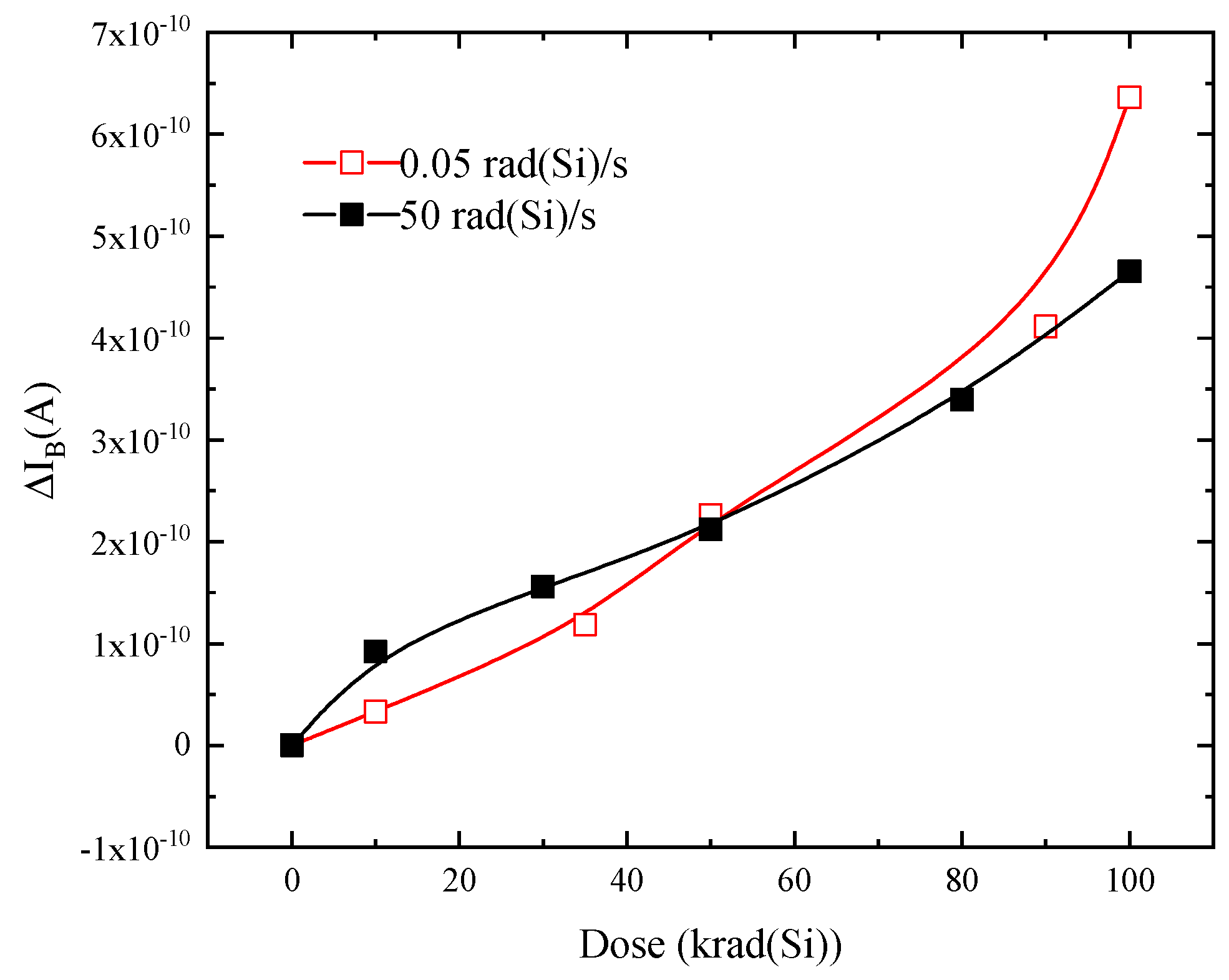
For comparison of the degradation level of the base current and the current gain under different dose rates, the excess base current Δ IB (ΔIB = IB − IB0) and normalized current gain β/β0, are introduced in the characterization analysis as shown in Figure 3 and Figure 4, where IB0, β0, IB and β are the base current and current gain before and after irradiation corresponding to VEB = 0.6 V, respectively. It can be seen in Figure 3 that when VEB = 0.6 V, ΔIB is increasing continuously with the accumulating total dose. When the irradiation dose increases up to 100 krad (Si), the base current IB increases by a value of 465 pA (ΔIB = 465 pA) for the high dose irradiation, while the increment of ΔIB is about 636 pA for the low dose rate, which is greater than the degradation under the high dose rate. Therefore, this PNP BJT fabricated with the DPSA technology may suffer from the ELDRS effect in the real and lower dose rate space irradiation environment, although the total degradation of the base current is slight. What is notable in Figure 3 is that the decrease of the base current under the high dose rate is above that irradiated with the low dose rate before the total dose reached 50 krad (Si). Moreover, for the first 50 krad (Si) irradiation, the increasing rate of ΔIB at the high dose rate is more rapid than irradiating at a low dose rate. It also shows the opposite increasing trend above the 50 krad (Si). For the final 10 krad (Si), the increasing speed of ΔIB soars up under the low dose rate and creates a relatively big gap between the high and low dose rate. These phenomena prove that the amounts of the interface trap charges in the Si/SiO2 interface dominate the attenuation of the base current under the long irradiation with a low dose rate condition [7].
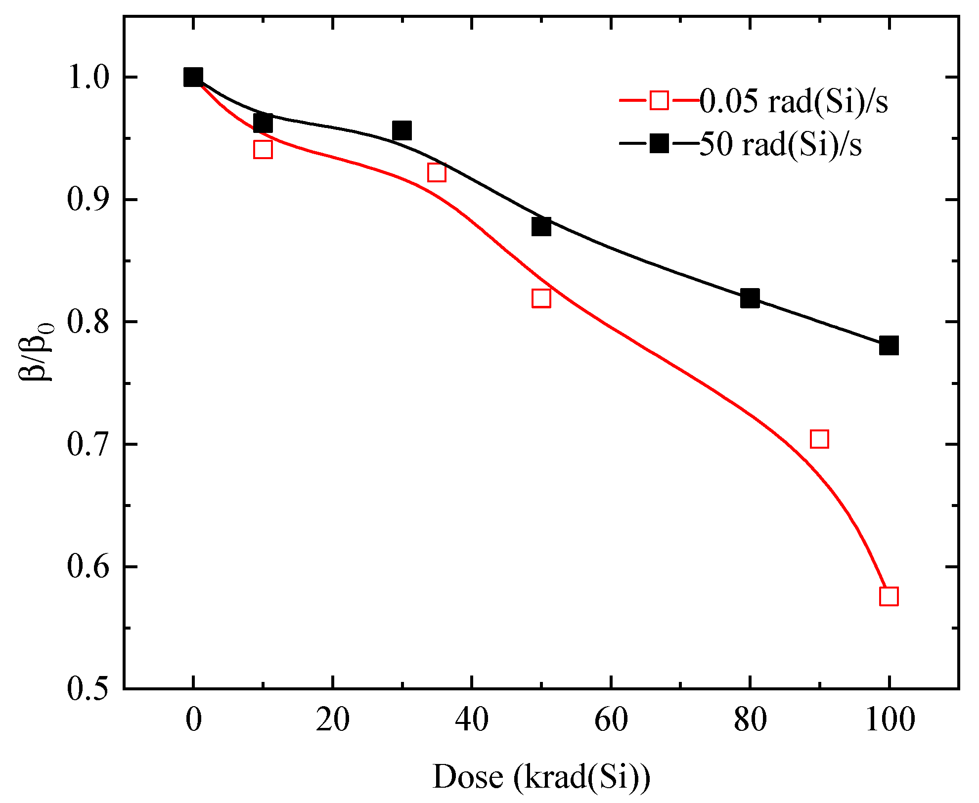
As the base current increases after irradiation, while the collector current remains basically unchanged, the degradation of the normalized current gain is finally shown in Figure 4. It can be seen clearly from the Figure that with the increase of the accumulated total dose, the current gains of the PNP BJTs all decrease rapidly. However, the declination rates are different between the high and low dose rate and consistent with the ΔIB depicted in Figure 3. The gain after high and low dose rate irradiation is reduced to 57.6% and 78% of the initial value, respectively. The results also show that the damage of the current gain under low dose rate irradiation is greater than that under a high dose rate, and will hence result in a potential ELDRS effect.
4. Discussion
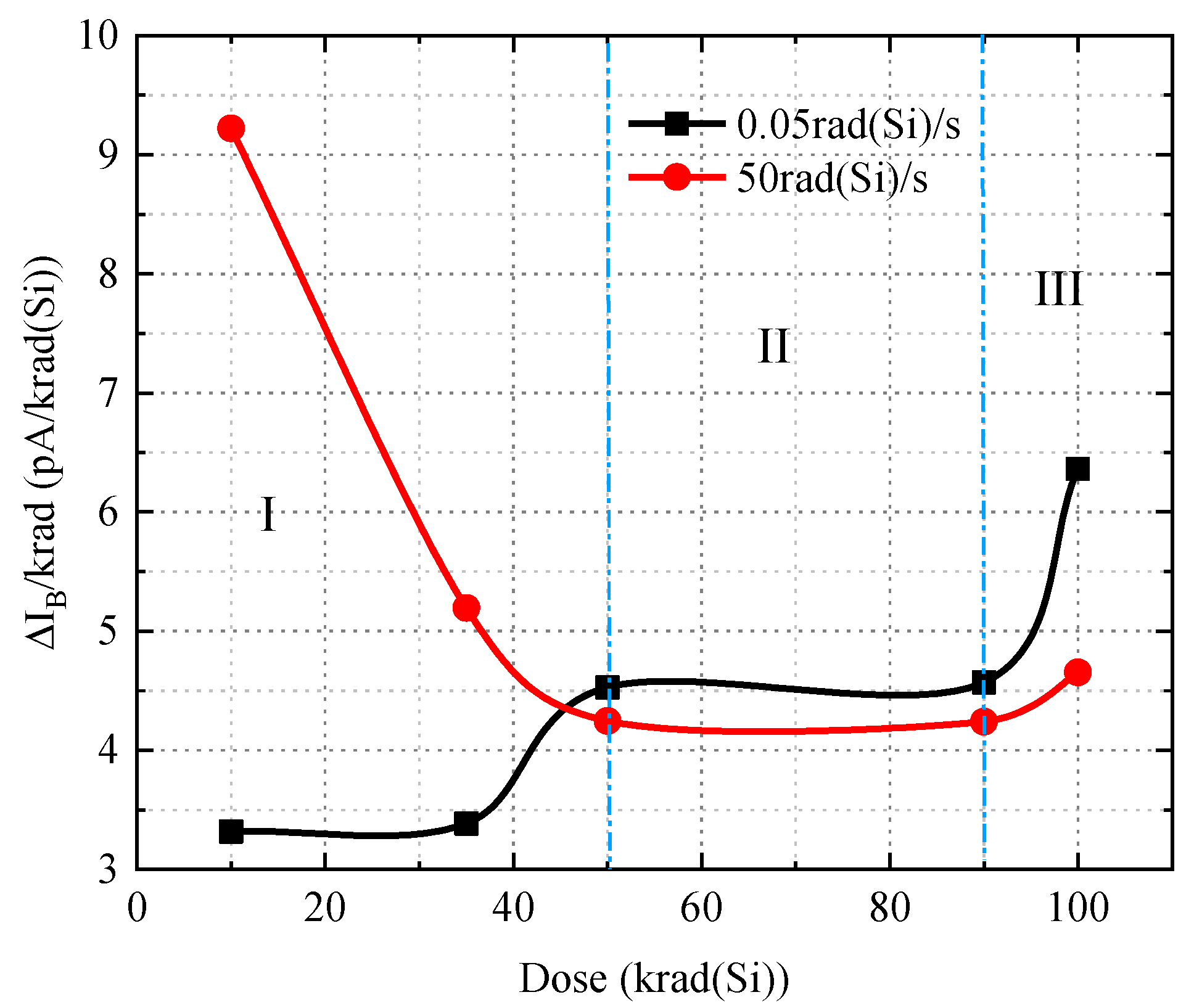
Figure 5 plots the degradation curve of the excess base current per unit krad (Si) irradiation dose of the DPSA BJTs to explain the radiation response processes mentioned above. Obviously, the degradation rate of the base current can be divided into three stages all through the irradiation process. For the beginning of the first stage, the degradation of the base current up to 10 pA per unit krad (Si) when the dose is accumulated to the first 10 krad (Si) at the high dose rate, and then with the total dose increases to 50 krad (Si), the degradation rate of the base current gradually descends and stabilizes to about 4.25 pA per krad (Si) degradation. On the contrary, under the low dose rate irradiation, the degradation rate of the excess base current was less than 3.5 pA at the initial 35 krad (Si) irradiation. After the dose reached 35 krad (Si) under the low dose rate, it begins to increase until 50 krad (Si), and then stayed as a constant of 4.5 pA/krad (Si) and a little bit above the degradation rate of 4.25 pA under the high dose rate irradiation, which is considered as the second stage in Figure 5.
The yield of the electron-hole pair under the high dose rate is much higher than that of low dose rate irradiation. A large number of oxide trap charges (, ) are generated by the combination of the holes () which escaped from the initial recombination with the electrons resulting in oxygen vacancies () and hydrogenated oxygen vacancies (, ) that are introduced in the manufacturing process by the following reactions [15,16]:
At the same time, long-term irradiation at a low dose rate contributes to the annealing of the oxide trap charge, and as a result, the initial value of the oxide trap charge is much higher than that of low dose rate irradiation, making the degradation rate of low dose rate irradiation much lower than that of high dose rate irradiation before 35 krad (Si). This explains the huge difference in degradation rate between high and low dose rates in the initial stage of irradiation. With the increase of irradiation time, the proton release reactions of the large amount of holes which escaped recombination under the low dose rate with the hydrogenated oxygen vacancies in the process of transport towards the Si/SiO2 interface [17] are dominated as shown in Equation (3) below. The released proton starts to arrive to the Si/SiO2 interface and reacts with the silicon dangling bond. The formation of the interface states begin at the accumulated total dose up to 35 krad (Si). Then, the degradation rate of the first stage increases under low dose rate irradiation. At the same time, the probability of recombination at high dose rates is increasing due to the very high concentrations of the electron-hole. Therefore, the proton release processes are being depressed and the interface trap charges are being reduced, which describe the declination of the degradation rate in Figure 5 under the high dose rate.
The space electric field induced by long-term irradiation at high dose rates is large enough to prevent the subsequent holes or hydrogen from being transported to the nearby interface to form deeper oxide trap charges and interfacial trap charges, while the shallow trap charges can be annealed under long-term room temperature irradiation [18,19]. Moreover, the dimerization of hydrogen increases gradually when the released protons react with the hydrogenated oxygen vacancies, with more and more accumulating ionizing total dose as shown in Equation (4). As discussed above, the degradation rate decreases and tends to be stable at the high dose rate. However, the competition between the stable increased interface trap charges and the annealing of low level oxide trap charges have predominated the degradation under the low dose rate. From Figure 5, it can be seen that the constant degradation rate of stage two is between the dose of 50 krad (Si) and 90 krad (Si), which may differ from process to process.
When the total dose is accumulated to 90 krad (Si), the degradation rate begins to increase significantly since the holes have enough time to transfer to the Si/SiO2 interface and form a large number of interface trapped charges [19]. However, the increases in degradation rates are different between the high and low dose rate as the amount of holes that reached the Si/SiO2 interface are not identical for the various dose rates [20,21]. There are more holes escaping from the initial electron-hole recombination being transported to the interface, where they release protons and then depassivate the Si dangling bonds [19,20,22] which are hydrogen passivated in the fabrication process, creating more interface trap charges under the low dose rate irradiation than at high dose rates. Furthermore, hydrogen molecules generated by the hydrogen dimer of Equation (4) will crack at the shallow oxide traps as shown in Equation (5) and behave as a source of protons, increasing the interface trap charge [23] and leading to an increase of degradation rate in the third stage under high dose rates.
5. Conclusions
In conclusion, this paper presents the gamma-ray radiation effect of DPSA PNP BJTs with a dose rate of 50 rad (Si)/s and 0.05 rad (Si)/s and discusses the mechanisms of different dose rate responses at different stages from the perspective of the degradation rate of the base current. The experimental results showed that the base current of the transistor did not change significantly under the irradiation conditions, showing a relatively good tolerance of radiation. The comparison of high and low dose rate showed that the increase of base current caused by low dose rate irradiation was larger than that caused by high dose rate irradiation, resulting in greater current gain degradation than that caused by high dose rate, highlighting that the ELDRS effect may occur. The three-stage degradation rate illustrated for the lower dose level of high dose rate irradiation demonstrate that the oxide trap charges are responsible for the rapid decrease. The competition of hole recombination by the electrons or captured by the traps resulted in a decrease of the degradation rate. As the competition reaches equilibrium, the degradation rate tends to be stable. The accumulated hydrogen molecular induced interface state is accountable for the increase of the degradation rate in the third stage for all irradiation dose rates.
Author Contributions
Conceptualization, W.L. and X.Y.; Data curation, M.L.; Formal analysis, M.L. and W.L.; Funding acquisition, W.L. and Q.G.; Investigation, M.L., X.L. and S.Y.; Methodology, W.L., X.Y., X.W., X.L. and S.Y.; Project administration, W.L. and X.Y.; Writing—original draft, M.L.
Funding
The work is supported by the National Natural Science Foundation of China (Grant No. U1532261).
Acknowledgments
The authors would like to acknowledge the great support offered by the staff of the Irradiation Center of the Xinjiang Technical Institute of Physics and Chemistry, Chinese Academy of Sciences.
Conflicts of Interest
The authors declare no conflict of interest.
References
- Miura-Mattausch, M.; Rüstig, J.; Kircher, R. Dependence of current gain β on spacer geometry and emitter size in polysilicon self-aligned bipolar transistors. Solid State Electron. 1990, 33, 325–331. [Google Scholar] [CrossRef]
- Glenn, J.; Neudeck, G. A Double Self-Aligned Silicon Bipolar Transistor Utilizing Selectively-Grown Single Crystal Extrinsic Contacts. Dep. Electr. Comput. Eng. Tech. Rep. 1992. [Google Scholar]
- Post, I.R.C.; Ashburn, P.; Wolstenholme, G.R. Polysilicon emitters for bipolar transistors: a review and re-evaluation of theory and experiment. IEEE Trans. Electron. Devices 1992, 39, 1717–1731. [Google Scholar] [CrossRef]
- Uchino, T.; Shiba, T.; Kikuchi, T.; Tamaki, Y.; Watanabe, A.; Kiyota, Y. Very-high-speed silicon bipolar transistors with in-situ doped polysilicon emitter and rapid vapor-phase doping base. IEEE Trans. Electron. Devices 1995, 42, 406–412. [Google Scholar] [CrossRef]
- Nakamura, T.; Nishizawa, H. Recent progress in bipolar transistor technology. IEEE Trans. Electron. Devices 1995, 42, 390–398. [Google Scholar] [CrossRef]
- Pease, R.L.; Schrimpf, R.D.; Fleetwood, D.M. ELDRS in Bipolar Linear Circuits: A Review. IEEE Trans. Nucl. Sci. 2009, 56, 1894–1908. [Google Scholar] [CrossRef]
- Fleetwood, D.M. Total Ionizing Dose Effects in MOS and Low-Dose-Rate-Sensitive Linear-Bipolar Devices. IEEE Trans. Nucl. Sci. 2013, 60, 1706–1730. [Google Scholar] [CrossRef]
- Flament, O.; Synold, S.; de Pontcharra, J.; Niel, S. Radiation tolerance of NPN bipolar technology with 30 GHz Ft. IEEE Trans. Nucl. Sci. 2000, 47, 654–658. [Google Scholar] [CrossRef]
- Graves, R.J.; Schmidt, D.M.; Kosier, S.L.; Wei, A.; Schrimpf, R.D.; Galloway, K.F. Visualization of ionizing-radiation and hot-carrier stress response of polysilicon emitter BJTs. In Proceedings of the 1994 IEEE International Electron Devices Meeting, San Francisco, CA, USA, 11–14 December 1994; pp. 233–236. [Google Scholar]
- Wu, X.; Zhang, P.; Tang, Z.; Tan, K.; Lu, W.; Jia, J. Reliability of DPSA bipolar junction transistors in radiation environment. In Proceedings of the International NanoElectronics Conference, INEC, Chengdu, China, 9–11 May 2016; pp. 1–2. [Google Scholar]
- Yi, Q.N.; Zhang, P.J.; Wu, X.; Chen, W.S.; Yang, Y.H.; Zhu, K.F.; Zhong, Y. Characteristics of ELDRS at high and low-level injection in double polysilicon self-aligned NPN bipolar transistors. In Proceedings of the 2016 13th IEEE International Conference on Solid-State and Integrated Circuit Technology (ICSICT), Hangzhou, China, 25–28 October 2016; pp. 1056–1058. [Google Scholar]
- Zhang, P.J.; Wu, X.; Jia, J.C.; Yi, Q.N.; Chen, W.S.; Yang, Y.H.; Zhu, K.F.; Lu, W.; Zhong, Y. A comparison of the reliability of 60Coγ ray irradiation on bulk-Si substrate and SOI substrate DPSA bipolar transistors. In Proceedings of the 2016 13th IEEE International Conference on Solid-State and Integrated Circuit Technology, ICSICT 2016, Hangzhou, China, 25–28 October 2016; pp. 1182–1184. [Google Scholar]
- Zhang, P.; Wu, X.; Yi, Q.; Chen, W.; Yang, Y.; Zhu, K.; Tan, K.; Zhong, Y. A comparison of the effects of cobalt-60 γ ray irradiation on DPSA bipolar transistors at high and low injection levels. Microelectron. Reliab. 2017, 71, 86–90. [Google Scholar] [CrossRef]
- Liu, M.; Lu, W. Dependence of emitter size on dose rate effect of double polysilicon self-aligned bipolar transistors. He Jishu/Nuclear Tech. 2018, 41, 1–5. [Google Scholar]
- Lenahan, P.M.; Dressendorfer, P.V. Hole traps and trivalent silicon centers in metal/oxide/silicon devices. J. Appl. Phys. 1984, 55, 3495–3499. [Google Scholar] [CrossRef]
- Freitag, R.K.; Brown, D.B.; Dozier, C.M. Experimental evidence of two species of radiation induced trapped positive charge. IEEE Trans. Nucl. Sci. 1993, 40, 1316–1322. [Google Scholar] [CrossRef] [Green Version]
- Graves, R.J.; Cirba, C.R.; Schrimpf, R.D.; Milanowski, R.J.; Michez, A.; Fleetwood, D.M.; Witczak, S.C.; Saigne, F. Modeling low-dose-rate effects in irradiated bipolar-base oxides. IEEE Trans. Nucl. Sci. 1998, 45, 2352–2360. [Google Scholar] [CrossRef] [Green Version]
- Boch, J.; Saigne, F.; Touboul, A.D.; Ducret, S.; Carlotti, J.F.; Bernard, M.; Schrimpf, R.D.; Wrobel, F.; Sarrabayrouse, G. Dose rate effects in bipolar oxides: Competition between trap filling and recombination. Appl. Phys. Lett. 2006, 88, 19–22. [Google Scholar] [CrossRef]
- Fleetwood, D.M.; Schrimpf, R.D.; Pantelides, S.T.; Pease, R.L.; Dunham, G.W. Electron Capture, Hydrogen Release, and Enhanced Gain Degradation in Linear Bipolar Devices. IEEE Trans. Nucl. Sci. 2008, 55, 2986–2991. [Google Scholar] [CrossRef]
- Rashkeev, S.N.; Fleetwood, D.M.; Schrimpf, R.D.; Pantelides, S.T. Effects of hydrogen motion on interface trap formation and annealing. IEEE Trans. Nucl. Sci. 2004, 51, 3158–3165. [Google Scholar] [CrossRef]
- Freitag, R.K.; Brown, D.B. Study of low-dose-rate radiation effects on commercial linear bipolar ICs. IEEE Trans. Nucl. Sci. 1998, 45, 2649–2658. [Google Scholar] [CrossRef] [Green Version]
- Boch, J.; Saign, F.; Schrimpf, R.D.; Vaill, J.-R.; Dusseau, L.; Lorfvre, E. Physical Model for the Low-Dose-Rate Effect in Bipolar Devices. IEEE Trans. Nucl. Sci. 2006, 53, 3655–3660. [Google Scholar] [CrossRef]
- Li, X.-L.; Lu, W.; Wang, X.; Yu, X.; Guo, Q.; Sun, J.; Liu, M.-H.; Yao, S.; Wei, X.-Y.; He, C.-F. Estimation of enhanced low dose rate sensitivity mechanisms using temperature switching irradiation on gate-controlled lateral PNP transistor. Chin. Phys. B 2018, 27, 036102. [Google Scholar] [CrossRef]
Figure 1.
The cross-section of theDPSA BJT.

Figure 2.
Gummel characteristics of a DPSA BJT before and after irradiation at the dose rate of 50 rad (Si)/s and 0.05 rad (Si)/s. VEB = emitter-base voltage; IC = collector current; IB = base current.
Figure 2.
Gummel characteristics of a DPSA BJT before and after irradiation at the dose rate of 50 rad (Si)/s and 0.05 rad (Si)/s. VEB = emitter-base voltage; IC = collector current; IB = base current.

Figure 3.
The excess base current of DPSA BJTs irradiated at a dose rate of 50 rad (Si)/s and 0.05 rad (Si)/s for PNP.
Figure 3.
The excess base current of DPSA BJTs irradiated at a dose rate of 50 rad (Si)/s and 0.05 rad (Si)/s for PNP.

Figure 4.
The normalized current gain of a DPSA BJT irradiated at the dose rate of 50 rad (Si)/s and 0.05 rad (Si)/s for PNP.
Figure 4.
The normalized current gain of a DPSA BJT irradiated at the dose rate of 50 rad (Si)/s and 0.05 rad (Si)/s for PNP.

Figure 5.
The degradation rate of the excess base current of a DPSA BJT under different dose rates.

© 2019 by the authors. Licensee MDPI, Basel, Switzerland. This article is an open access article distributed under the terms and conditions of the Creative Commons Attribution (CC BY) license (http://creativecommons.org/licenses/by/4.0/).
Share and Cite
MDPI and ACS Style
Liu, M.; Lu, W.; Yu, X.; Wang, X.; Li, X.; Yao, S.; Guo, Q. Mechanism of Degradation Rate on the Irradiated Double-Polysilicon Self-Aligned Bipolar Transistor. Electronics 2019, 8, 657. https://doi.org/10.3390/electronics8060657
AMA Style
Liu M, Lu W, Yu X, Wang X, Li X, Yao S, Guo Q. Mechanism of Degradation Rate on the Irradiated Double-Polysilicon Self-Aligned Bipolar Transistor. Electronics. 2019; 8(6):657. https://doi.org/10.3390/electronics8060657
Chicago/Turabian StyleLiu, Mohan, Wu Lu, Xin Yu, Xin Wang, Xiaolong Li, Shuai Yao, and Qi Guo. 2019. "Mechanism of Degradation Rate on the Irradiated Double-Polysilicon Self-Aligned Bipolar Transistor" Electronics 8, no. 6: 657. https://doi.org/10.3390/electronics8060657
Note that from the first issue of 2016, this journal uses article numbers instead of page numbers. See further details here.