Decoupling Capacitors Placement at Board Level Adopting a Nature-Inspired Algorithm
by
 , , and
Stefano Piersanti
1, 
Riccardo Cecchetti
1,
Carlo Olivieri
1,
Francesco de Paulis
1 ,
,
Antonio Orlandi
1,* and
and
Markus Buecker
2 1
UAq EMC Laboratory, Department of Industrial and Information Engineering and Economics, University of L’Aquila, L’Aquila 64100, Italy
2
Zuken GmbH, 33104 Paderborn, Germany
*
Author to whom correspondence should be addressed.
Electronics 2019, 8(7), 737; https://doi.org/10.3390/electronics8070737
Submission received: 12 June 2019
/
Accepted: 26 June 2019
/
Published: 29 June 2019
(This article belongs to the Section Computer Science & Engineering)
Abstract
:Decoupling capacitors are fundamental keys for the reduction of transient noise in power delivery networks; their arrangement and values are crucial for reaching this goal. This work deals with the optimization of the decoupling capacitors of a power delivery network by using a nature-inspired algorithm. In particular, the capacitance value and the location of three decoupling capacitors are optimized in order to obtain an input impedance below a specific mask, by using a nature-inspired algorithm, the genetic one, in combination with two electromagnetic solvers used to compute the objective function. An experimental board is designed and manufactured; measurements are performed to validate the numerical results.
1. Introduction
The requests, coming from the market and incorporated by the industry, are more and more steered toward a miniaturization of the devices with the target to improve their performances. All these efforts are not costless: Shrinking the device dimensions implies a non-negligible number of problems such as degradation of the signal quality, increase in heat dissipation problems, and manufacturing complexity. All these aspects result in a collection of power and signal integrity issues [1,2].
Among the several causes that can lead to signal integrity (SI) problems, the power integrity (PI) related to the power/ground supply voltage at board level is one of the central requirements of modern design; having a power distribution network (PDN) defined by a high inductance or spending not enough time and effort on the PDN impedance design can cause severe PI issues [3]. Adopting decoupling capacitances (decaps) [4] is an effective solution in the optic of the reduction of transient noise caused by voltage droop due to the switching currents. A manual placement of decaps can lead to not optimal solution and can be time consuming; for these reasons, CAD tools and new algorithms [5,6,7,8] try to propose automatic procedures for the decaps arrangement. However, handling a large amount of decaps can lead to an increase of the power consumption, to reliability issues, and to a decrease of component space available on board [9]. As a result, a trade-off between the number of decaps, as well as their values, and their proper arrangement on board is a must for today’s board design to fulfill all the requirements.
At the early stage of a printed circuit board (PCB) design and in particular its PDN, an optimization procedure might help and assist the designers providing a powerful tool from the selection of the electrical and geometrical parameters of the stack-up, to the appropriate placement of each decaps. This convenient and rational design aims to drastically reduce the signal and power integrity issues.
The nature-inspired algorithms (NIAs) [10,11] are a class of optimization algorithms inspired by natural mechanisms. They also include particle swarm optimization (PSO) [12], evolutionary algorithms (EA) [12], and genetic algorithms (GA) [13,14]. PSO is a population-based stochastic optimization technique; compared to EA and GA, the advantages of PSO are that it is easy to implement and there are few parameters to adjust. At the same time, not having evolution operators such as crossover and mutation, its efficiency in exploring the solution domain of the considered problem is limited. On the other hand, for the considered application, EA and GA have shown the highest efficiency from the computational point of view. Between them, GAs have a simpler architecture of the code. Computational efficiency and software architecture simplicity have stirred the choice of GAs as optimization algorithm for this work. The aim of this work is to explore, starting from simple configurations, the use of GAs as suitable algorithms for the optimization of the decoupling capacitance on a PDN at board level. In the following, a GA is adopted for finding the optimum number and values of decaps to be mounted on a simple PDN of a printed circuit board (PCB) with the goal to have an input impedance of the PDN below a specific mask selected by the designer based on the design specifications. The input impedance is evaluated through two different tools: EZpp [15,16,17] and PI/EMI analysis module within design force (from now on named “DF PI”) (by Zuken [18]). The results will be the base for more realistic and complex analysis that will be carried out in the continuation of this research.
The paper is organized as follow: Section 2 describes the test board, in terms of geometry, stack-up, and materials. In the same section, there is a part concerning the main differences between the two solvers EZpp and DF PI. Section 3 is devoted to the GA describing the steps composing the algorithm. Section 4 shows the results of the optimization of decaps value; Section 5 reports the results of the optimization of both decaps value and their position. In Section 6, the proposed approach is validated by comparing the computed results with those measured on a specifically designed PDN board. Finally Section 7 discusses the significant outcomes and introduces the future steps of this research.
2. Overview of the Test Board
The test structure considered in this investigation, as shown in Figure 1, is a two-layer board built by two copper planes (electrical conductivity σcu = 58 MS/m, thickness tcu = 0.03 mm) representing a PDN with power (PWR) and ground (GND) planes, separated by a FR4 dielectric slab (relative dielectric permittivity εr = 4.3, loss tangent tgδ = 0.02, thickness tFR4 = 0.25 mm).
Figure 1 also shows the port P, from which the input impedance Zin of the PDN is evaluated during the optimization process. The target of the optimization is to find suitable values for the capacitances of Npos = 3 decaps (C1, C2, C3) placed at fixed positions near the input port P (blue squares in Figure 1a). In Section 5, the position of the decaps will become an optimization variable. Capacitors’ parasitic inductance (ESL) and resistance (ESR) are kept fixed and equal to 50 nH and 30 mΩ, respectively. These stray parameters can be considered a sort of average values among those associated to the 0603 to the 0805 packages of the AVX Y5V series. The coordinates of the input port P and of the three decaps are summarized in Table 1.
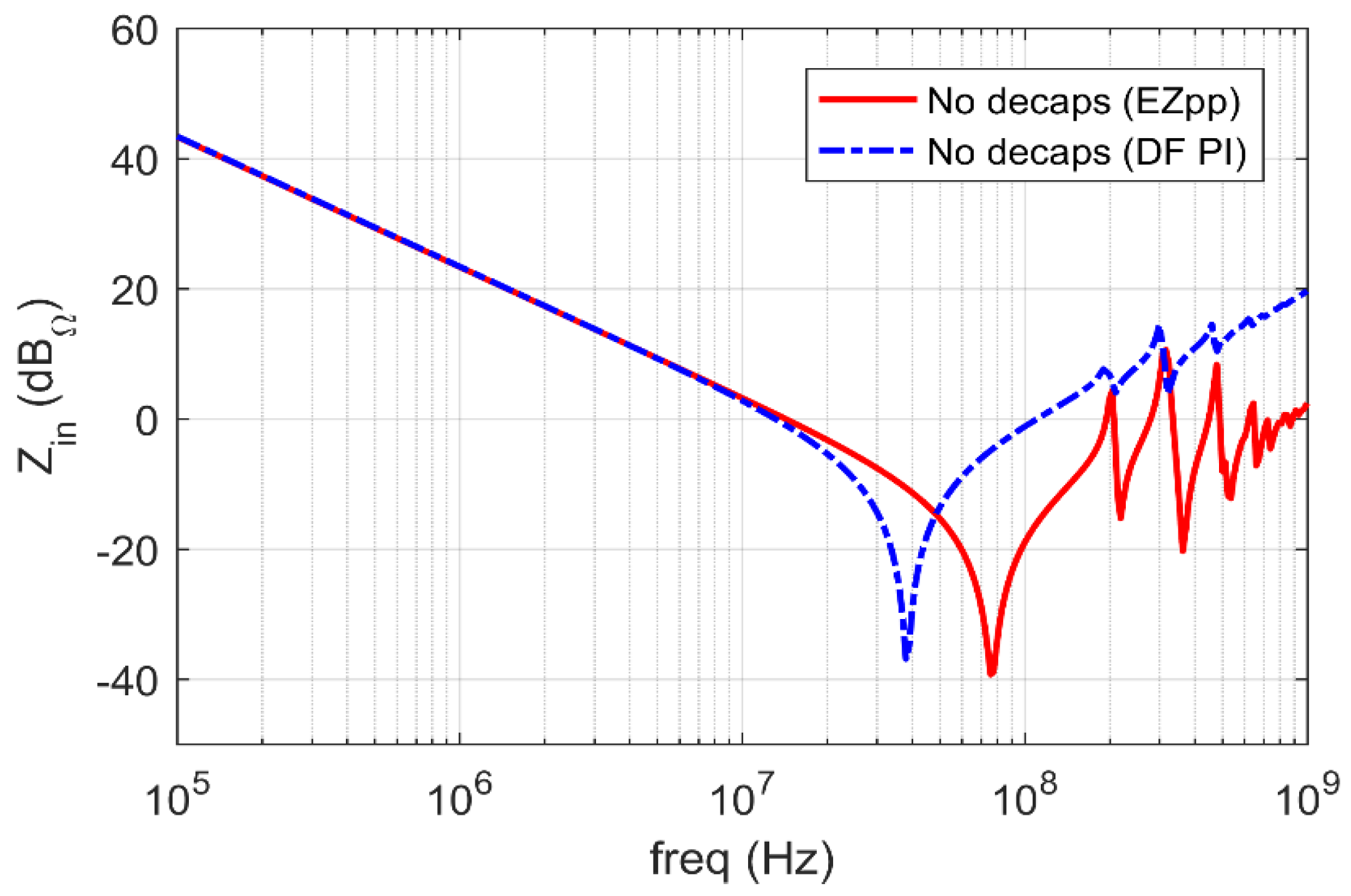
Before proceeding with the optimization task, a comparison between the outputs from EZpp and those from DF PI has been done in order to detect the possible differences between the results. Consequently, the Zin without decoupling capacitances has been computed by the two solvers and compared (Figure 2). Up to almost 50 MHz, the predominant factor is the capacitance of the planes, as justified by the capacitive trend of Zin at low frequency. The equivalent capacitance can be quantified as:
where ε0 is the vacuum permittivity, A is the area of the board and tFR4 = 0.25 mm is the distance between the two planes. EZpp and DF PI provide a capacitance value very close to Equation (1), as reported in Table 2.
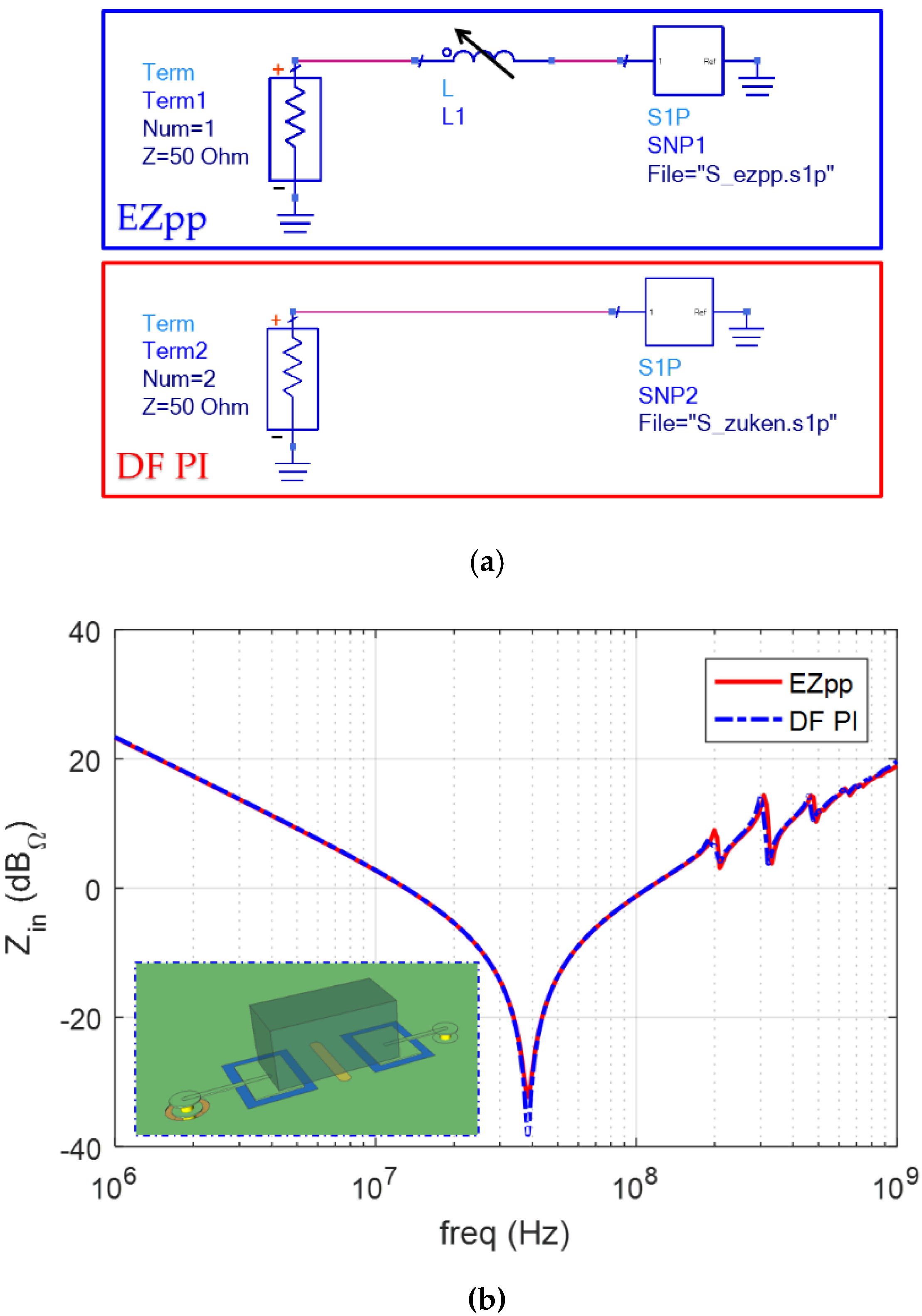
The largest difference between the results from the two solvers can be appreciated at high frequency, where Zin from DF PI exhibits an excess of inductance with respect to that from EZpp. This inductance can be quantified importing, in the circuit simulator Advanced Design System (ADS) [19], the S-parameters from the simulations without decaps and then adding a tunable series inductance between the termination port and the S-Parameter block of the circuit associated to the EZpp results, as depicted in Figure 3a. Tuning the inductance L1, the matching between the frequency spectra of the input impedance from the two solvers (Figure 3b) is reached using an inductance of L1 = 1.20 nH. According to the IEEE Standard P1597 [20], the feature selective validation technique [20,21,22] is used to quantify the matching of the two curves in Figure 3b. The matching is classified as “excellent” [20] being the FSV figure of merits GRADE = 1 and SPREAD = 1.
The extra inductance L1 is introduced by the DF PI model due to the presence of traces and vias (see inset of Figure 3b), which create the connections of each component with the GND and PWR planes.
3. Implementation of the Optimization Algorithms
The NIA chosen to optimize the capacitance values of the three capacitors is the genetic algorithm (GA) [13,14] inspired by the principles of natural selection. The aim of this section is to briefly describe how this algorithm works and how it is interfaced with the two tools, EZpp and DF PI.
3.1. The Genetic Algorithm
The genetic algorithm is a technique allowing a population, composed by Np so-called chromosomes (chrom), to evolve according to specific laws toward a state able to minimize a cost function. The cost function fcost is a mathematical function whose input is each chromosome of the population and the output is generally a value used for creating a rank among the Np chromosomes; in this work, the fcost is defined as follows:
where N1 is the number of the frequency points (361 in the specific case) of Zin that are larger than a specific mask, Zmask (Figure 5), defined by the user, and N2 is the area between the mask and Zin. The factor 107 is introduced in order to avoid that N2 becomes predominant with respect N1.
The target of a GA is to find a vector (chromosome) of Ng = 3 entries (genes) as,
representing the capacitance of three decaps placed around P in a fixed position according to Figure 1a.
The objective of the GA is to minimize fcost; that is to say, to find the best member of the population, chrombest, able to provide the smallest fcost as possible.
The first step of the GA is the definition of the initial population, composed by Np chromosomes, chosen by a random technique [13] from a minimum value, Cmin = 10 nF, and a maximum value, Cmax = 1 µF, resulting in a Np × Ng matrix. The next step is the selection: For each chromosome, the algorithm evaluates the cost function and ranks the population from the fittest (lowest fcost) to the unfittest (highest fcost) electing the best ones for the next step. The number of chromosomes discarded is selected through the variable Xr: The discarded chromosomes are deleted. In the present study, Xr = 0.5, meaning that half population survives, forming the mating pool, and it will be used for the generation of the offspring replacing the discarded chromosomes. Through a “Roulette Wheel” procedure [13], a pair of chromosomes is chosen for generating a pair of offspring; this procedure, called mating, takes place until all the Xr∙Np discarded chromosomes are replaced. The crossover point is randomly chosen between the first and the last genes of the parents’ chromosomes; in this way, each parent donates part of its genes to the resulting offspring.
The subsequent step is the mutation, whose purpose is to introduce diversity in the population randomly altering one or more genes. The number of mutations is regulated by the mutation factor µ which, in the present study, is chosen as µ = 20%.
Once the mutation is applied, the cost function of the brand-new population is evaluated again. The entire procedure, described so far, is iterated until the maximum number of generations (maxgen) is reached or the convergence is reached (fcost = 0). The outcome is the optimum values of the three capacitances C1, C2, C3.
3.2. Optimization Flow Using EZpp and DF PI
The genetic algorithm described in the previous subsection is implemented by using EZpp and DF PI as computational engines and is depicted in Figure 6a,b, respectively.
EZpp [17] is a tool, developed at the EMC Laboratory of the University of Missouri Science and Technology, based on a cavity model [15,16] able to find the S- and Z-Parameters of a PDN, once adding decoupling capacitors at any location over the board itself. All the geometrical and electrical parameters of the board, as well as the locations of input port and decaps, are stored in a text file (.ppf file).
On the other hand, DF PI by Zuken is a 3D PCB design suite which allows to draw the board, define material properties, and place components, selected from a vast library. The PI/EMI analysis tool engine implemented inside DF PI is able to provide the profile of the Zin at the input port, as well as its spatial distribution, for specified frequencies.
The two flows in Figure 6a,b have similarities and differences. The main similarity is in their architecture: The logical position of the launching of the computational engine (EZpp or DF PI) for the evaluation of the cost function is the same to ensure a degree of uniformity in the software structure when the computational engine changes. The main difference between the two flows is how the software handles their input. Concerning EZpp, the Np chromosomes forming the populations are written inside the Np single.ppf files and used as input for EZpp. The resulting Np input impedances, as .csv files, are compared with the mask for obtaining the cost function. Instead, DF PI introduces more flexibility: The entire population, composed by Np chromosomes is written in a single .xml file which, through a batch procedure, is read by DF PI for the generation of as many input impedances.
4. Optimization of the Decoupling Capacitance Value
Figure 7a shows the result of the optimization using EZpp when the maximum number of generations is maxgen = 10 and is maxgen = 100. The resulting input impedances are very similar except at low frequency, around 2 MHz, where the Zin from 10 generations exhibits a peak crossing the mask. As a consequence the case with maxgen = 10 is characterized by a higher fcost, as confirmed by Table 3. The optimum value for the capacitor C1, C1,opt, is very similar in both cases, confirming that the closest capacitor to the input port has the highest impact on the input impedance. In the direction of identify the optimal trade-off between computational time and accuracy of the solution, one can adjust the number of the maximum generations maxgen: The higher the value of maxgen, the lower the value of fcost; all this process is translated in an increasing of the computational time for the optimization algorithm. In the present case, maxgen = 100 introduces a slight improvement, in terms of Zin, at low frequencies, where the capacitances have more effect.
Adopting DF PI as solver for the optimization gives a Zin as illustrated in Figure 8a. Also in this case, there is a slight difference between maxgen = 10 and maxgen = 100, at low frequency. The main difference with respect to EZpp is an aftermath of the excess inductance discussed in Section 2. This has a huge impact on the value of fcost, especially for N2. A higher inductance implies a higher value of the impedance at high frequency, which means a larger value of the area between the mask and the Zin resulting from the optimization, so explaining the higher value of fcost, reported in Table 4, with respect the values from EZpp in Figure 7. Figure 8b testifies, once again, how an increase of the maxgen causes a decreasing of fcost.
5. Optimization of Decaps Value and Position
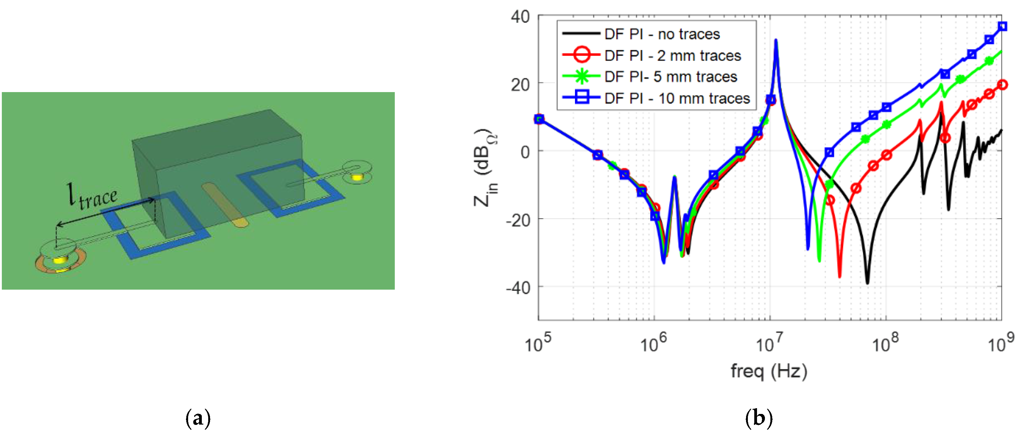
The previous section is devoted to the optimization of the value of three decaps, when their position is fixed. The same algorithm used for this task can be adapted for the optimization of the three decaps value as well as their position on the board. Different from the previous scenario, now the decaps values cannot vary from a minimum value (Cmin = 10 nF) and a maximum value (Cmax = 1 µF) in a continuous way, but in discrete steps. Defined Celem = 100 nF (ESR = 30 mΩ; ESL = 50 nH) as an elementary capacitance, in each of the Npos = 3 positions the algorithm can place from Ndec,min = 1 to Ndec,max = 5 elementary capacitances in parallel. The positions on the boards are not arbitrary, but they are uniformly distributed on a grid, as depicted in Figure 9a. Additional relevant difference concerns the solver DF PI: As described in previous sections, because of the presence of 2 mm traces connecting the capacitance component to the vias, Zin coming from DF PI exhibits higher inductance compared with the Zin from EZpp, which does not take into account neither vias and traces. So, in the direction of carrying on a more consistent comparison between the two solvers, the 2 mm traces have been deleted and now the capacitor is directly connected with PWR and GND planes through vias (Figure 9b).
The i-th chromosome has the following form:
where Pos1, Pos2, Pos3 represent three of the 52 possible grid positions and Ndec,C1, Ndec,C2, and Ndec,C3 are the number of elementary capacitors in each position.
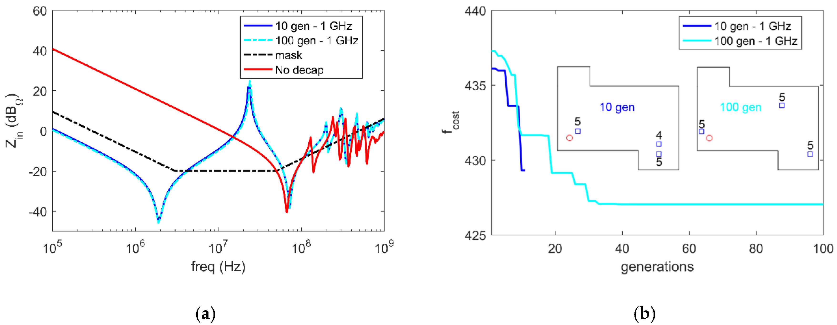
Figure 10a and Figure 11a show the output of the optimization, for maxgen = 10 and maxgen = 100, by using as computational engines EZpp and DF PI, respectively. Both solvers are able to fulfill the condition of an input impedance under the mask, especially at low frequency where the decaps are more effective. Increasing the number of maximum generations from 10 to 100 leads to a slight improvement in terms of cost function: 427 to 429 for DF PI and 326 to 330 for EZpp, as shown by Figure 10b and Figure 11b. The insets in the same figures present the positions and the number of elementary decaps chosen by the GA. The placement resulting from EZpp sees the decaps closer to the input port with respect the position given by the optimization using DF PI. However, both solvers choose a number of decaps very close to the maximum Ndec,max = 5 and, more relevant, at least one position in the proximity of the input port P.
As mentioned, the benefit of decaps on the input impedance is more evident at low frequency so an optimization limited to fmax = 10 MHz has been carried out to better exploit the performances of EZpp and FD PI. Figure 12a and Figure 13a show the profile of Zin obtained by the two above-mentioned computational engines.
When fmax = 1 GHz, due to the numerous resonances at high frequency, Zin tends to more easily change its profile with the variation of number and position of the decaps and a stable cost function is reached after the 40th generation; when the optimization is limited up to fmax = 10 MHz, the convergence of the cost function is reached only after 20 generations as shown in Table 5. In addition, now the placement emerging from the optimization is characterized by decaps closer to the input port (Figure 12b and Figure 13b). Finally, a remark on the computational efficiency. The two relevant parameters considered are the convergence (the number of generations needed to have a constant cost function) and the CPU time. In all cases considered, the maximum number of generations needed for convergence is a little less than 100 (Figure 8b) with an average of 49 over all test performed. This indicates that the implemented GA properly covers the search space. The maximum computational time for 100 generations is 109 min, including the plot and storage of the results.
6. Measurements
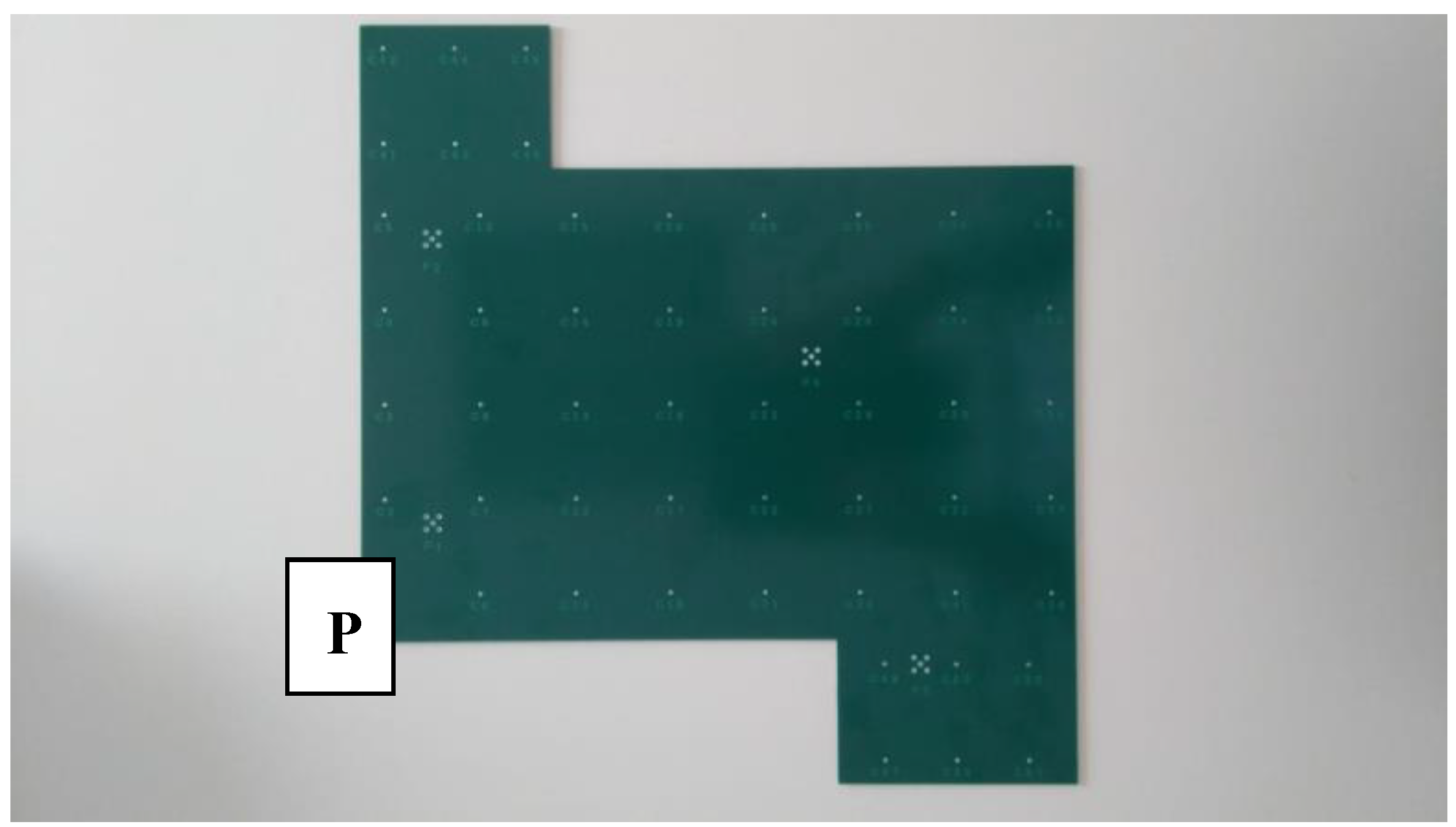
In order to support the results of this work (and also those related to the next steps of the project as indicated in the next section), a test vehicle of a PDN board has been designed and manufactured, whose geometry and electrical characteristics are similar to that described in Section 2 and Section 5. Figure 14 shows the top view of the manufactured board in which either the footprint of the SMA connectors (ports) and the grid of pads for the decoupling capacitors are visible (as illustrated in Figure 9a).
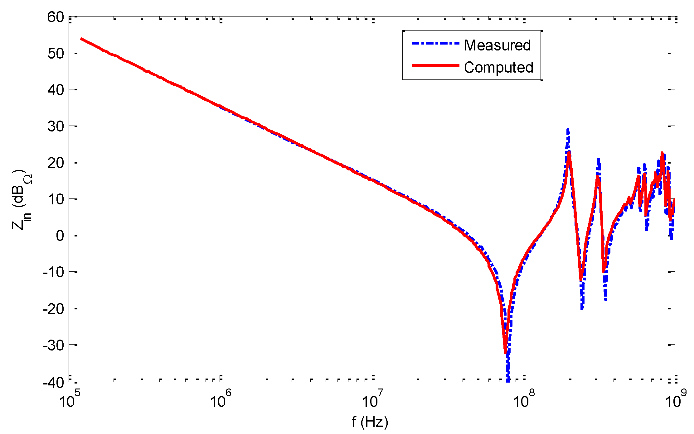
As a first check, the input impedance at the left bottom port P of the PDN board without capacitors (bare board) has been measured paying attention to also de-embed the mainly inductive effects of the connector. The comparison between the frequency spectrum of the magnitude of the measured input impedance and the same impedance computed by DF PI (the computational engine of the proposed optimization procedure) is shown in Figure 15.
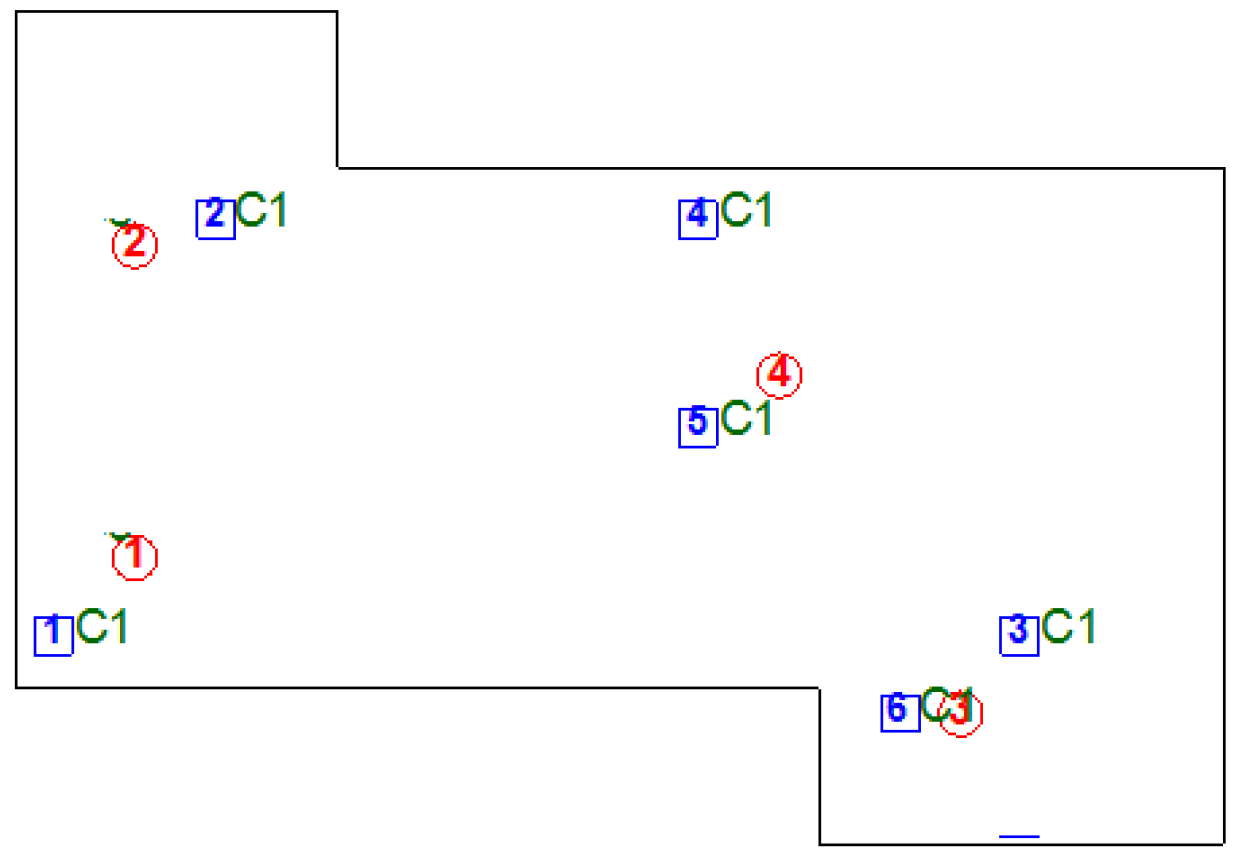
After having run an optimization instance, the proposed algorithm generates the positions of six decoupling capacitors as indicated in Figure 16.
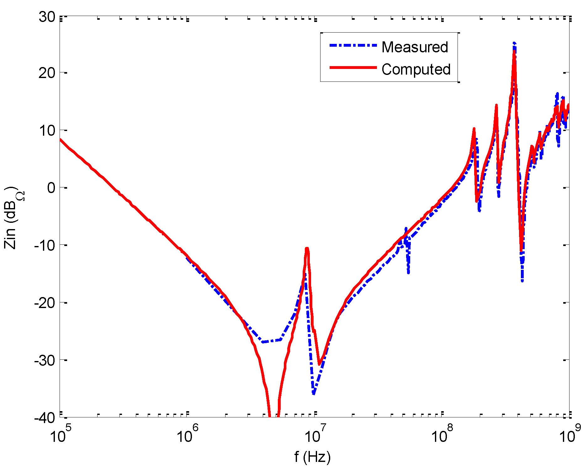
Figure 17 shows the comparison of the measured frequency spectrum of the magnitude of the input impedance of the PDN board with the decoupling capacitors mounted as in Figure 16 and the corresponding computed values.
From Figure 17, it appears that the proposed computational procedure is able to catch either the low-frequency (capacitive) behavior of the PDN board or its high-frequency (inductive) one. Between 100 MHz and 1 GHz, the resonant modes of the physical board are well matched with those computed. The number of measured frequency point is less than the number of computed one. This is the reason for the difference of depth between the two notches at around 5 GHz.
7. Conclusions
Decoupling capacitance is used for the reduction of transient noise in power supply network, but at the same time, a redundant number of them can lead to a considerable series of design issues. A systematic procedure for decaps quantification and placing has to be followed at different steps of the design. This work applies a nature-inspired algorithm to the definition of the decoupling capacitors on a PDN. The optimal position, the number of elementary decaps, and some figures of merit of the algorithm (such as the minimum significant number of generations) are evaluated using a GA, in cooperation with two software tools, EZpp and DF PI. Both software tools are suitable calculation engines; they are able to provide an optimal solution in a limited number of iterations with a very limited difference in their results, cross validating each other.
The computed numerical results in terms of the frequency spectrum of the input impedance are validated by means of the comparison with the measured values of the same impedance measured on a specifically designed PDN board.
The next steps of this research project target to apply the proposed procedure to the design of a real and more complex PDN considering some constraints in the cost function (such as minimum number of decaps, reliability issues, weight) and to introduce an artificial neural network (ANN), which will be able, once properly trained, to replace the use of complex software calculations engines as EZpp and DF PI, with a direct impact in the reduction of the simulation and optimization time.
Author Contributions
Conceptualization, A.O. and M.B.; methodology, A.O. and F.d.P.; software, S.P., C.O., and R.C.; validation, F.d.P. and C.O.; writing—original draft preparation, A.O. and S.P.; writing—review and editing, A.O. and F.d.P.
Funding
This research was funded by Google, 2017 Google Faculty Research Award.
Acknowledgements
The authors would like to thank Zhiping Yang at Google for his valuable support, the useful discussions and the insightful comments for the development of this work.
Conflicts of Interest
The authors declare no conflict of interest.
References
- Hall, S.H.; Heck, H.L. Advanced Signal Integrity for High-Speed Digital Designs; Wiley: New York, NY, USA, 2009. [Google Scholar]
- Orlandi, A.; Archambeault, B.; de Paulis, F.; Connor, S. Electromagnetic Bandgap (EBG) Structures. Common Mode Filters for High Speed Digital Systems; IEEE Press/Wiley: New York, NY, USA, 2017. [Google Scholar]
- Swaminathan, M.; Han, K.J. Design and Modeling for 3D ICs and Interposers; World Sci.: Singapore, 2014. [Google Scholar]
- Smith, L.D.; Bogatin, E. Principles of Power Integrity for PDN Design; Prentice-Hall: New York, NY, USA, 2016. [Google Scholar]
- Su, H.; Sapatnekar, S.S.; Nassif, S.R. Optimal decoupling capacitor sizing and placement for standard-cell layout designs. IEEE Trans. Comput. Aided Des. Integr. Circuits Syst. 2003, 22, 428–436. [Google Scholar] [CrossRef]
- Wang, X.; Cai, Y.; Zhou, Q.; Tan, S.X.; Eguia, T. Decoupling Capacitance Efficient Placement for Reducing Transient Power Supply Noise. In Proceedings of the IEEE/ACM International Conference on Computer-Aided Design—Digest of Technical Papers, San Jose, CA, USA, 2–5 November 2009; pp. 745–751. [Google Scholar]
- Han, G. Simple and Fast method of On-Board Decoupling Capacitor Selection and Placement. In Proceedings of the IEEE Electrical Design of Advanced Packaging and Systems Symposium (EDAPS), Haining, China, 14–16 December 2017; pp. 1–3. [Google Scholar] [CrossRef]
- Piersanti, S.; de Paulis, F.; Olivieri, C.; Orlandi, A. Decoupling Capacitors Placement for a Multichip PDN by a Nature-Inspired Algorithm. IEEE Trans. Electromagn. Compat. 2018, 60, 1678–1685. [Google Scholar] [CrossRef]
- Im, S.; Srivastava, N.; Banerjee, K.; Goodson, K.E. Goodson. Scaling analysis of multilevel interconnect temperatures for high-performance ICs. IEEE Trans. Electron Devices 2005, 52, 2710–2719. [Google Scholar] [CrossRef]
- Patnaik, S.; Yang, X.; Nakamatsu, K. Nature-Inspired Computing and Optimization; Springer: Zurich, Switzerland, 2016. [Google Scholar]
- Koziel, S.; Leifsson, L.; Yang, X. Simulation-Driven Modeling and Optimization; Springer: Zurich, Switzerland, 2016. [Google Scholar]
- Liang, J.J.; Qin, A.K.; Suganthan, P.N.; Baskar, S. Comprehensive learning particle swarm optimizer for global optimization of multimodal functions. IEEE Trans. Evol. Comput. 2006, 10, 281–295. [Google Scholar] [CrossRef]
- Haupt, R.L.; Haupt, S.E. Practical Genetic Algorithms, 2nd ed.; Wiley: New York, NY, USA, 2004. [Google Scholar]
- Haupt, R.L.; Werner, D.H. Genetic Algorithms in Electromagnetics; Wiley: New York, NY, USA, 2007. [Google Scholar]
- Zamek, I.; Boyle, P.; Li, Z.; Sun, S.; Chen, X.; Chandra, S.; Li, T. Modeling FPGA Current Waveform and Spectrum and PDN Noise Estimation. In Proceedings of the DesignCon 2008, Santa Clara, CA, USA, 4–7 February 2008. [Google Scholar]
- Lei, G.; Techentin, R.W.; Gilbert, B.K. High-frequency characterization of power/ground-plane structures. IEEE Trans. Microw. Theory Technol. 1999, 47, 562–565. [Google Scholar]
- EMS+, EZPP User Manual. Available online: www.ems-plus.com (accessed on 2 November 2018).
- Zuken, Design Force User Manual. Available online: https://www.zuken.com/it/products/pcb-design/cr-8000/products/design-force 69 (accessed on 2 November 2018).
- Advanced Design System (ADS) 2013. Available online: www.keysight.com/en/pc-1297113/advanced-design-system-ads (accessed on 2 November 2018).
- Institute of Electrical and Electronics Engineers. IEEE Standard P1597, Standard for Validation of Computational Electromagnetics Computer Modeling and Simulation—Part 1; Institute of Electrical and Electronics Engineers: Piscataway, NJ, USA, 2008. [Google Scholar]
- Duffy, A.P.; Martin, A.J.M.; Orlandi, A.; Antonini, G.; Benson, T.M.; Woolfson, M.S. Feature Selective Validation (FSV) for validation of computational electromagnetics (CEM). Part I—The FSV method. IEEE Trans. Electromagn. Compat. 2006, 48, 449–459. [Google Scholar] [CrossRef]
- Orlandi, A.; Duffy, A.P.; Archambeault, B.; Antonini, G.; Coleby, D.E.; Connor, S. Feature Selective Validation (FSV) for validation of computational electromagnetics (CEM). Part II—Assessment of FSV performance. IEEE Trans. Electromagn. Compat. 2006, 48, 460–467. [Google Scholar] [CrossRef]
Figure 1.
(a) Test boards and (b) its stack-up. The red circle represents the input port P from which the input impedance Zin in evaluated by EZpp and design force (DF) power integrity (PI), whereas C1, C2, and C3 are the three decoupling capacitors whose values have to be optimized by the genetic algorithm (GA).

Figure 2.
Zin computed without decoupling capacitances by EZpp (red line) and from DF PI (blue line).
Figure 2.
Zin computed without decoupling capacitances by EZpp (red line) and from DF PI (blue line).

Figure 3.
(a) Circuits used in ADS for tuning the inductance L1 in order to match Zin, without decaps, from EZpp with the one from DF PI, getting the profiles shown in (b). The inset shows how a component, in this case a capacitor, is represented by DF PI with traces and vias creating the connection with PWR and GND planes.

Figure 4.
(a) Trace, whose length is ltrace, connecting the port to the vias and (b) Zin computed by DF PI when the ltrace is changed from 0 to 10 mm.
Figure 4.
(a) Trace, whose length is ltrace, connecting the port to the vias and (b) Zin computed by DF PI when the ltrace is changed from 0 to 10 mm.

Figure 5.
Zmask delineating the upper limit for the input impedance Zin of the board.

Figure 6.
Optimization flow for (a) EZpp and (b) DF PI.

Figure 7.
(a) Result of the optimization in EZpp after 10 generations (solid red line) and 100 generations (dotted–dashed green line) compared with the mask and the case without decaps. (b) Cost function fcost as function of the number of generations when maxgen = 10 and maxgen = 100.
Figure 7.
(a) Result of the optimization in EZpp after 10 generations (solid red line) and 100 generations (dotted–dashed green line) compared with the mask and the case without decaps. (b) Cost function fcost as function of the number of generations when maxgen = 10 and maxgen = 100.

Figure 8.
(a) Result of the optimization in DF PI after 10 generations (solid red line) and 100 generations (dotted–dashed green line) compared with the mask and the case without decaps. (b) Cost function fcost as function of the number of generations when maxgen = 10 and maxgen = 100.
Figure 8.
(a) Result of the optimization in DF PI after 10 generations (solid red line) and 100 generations (dotted–dashed green line) compared with the mask and the case without decaps. (b) Cost function fcost as function of the number of generations when maxgen = 10 and maxgen = 100.

Figure 9.
(a) Possible positions for the decaps over the board and (b) new configuration for the capacitor in DF PI having no traces for the connection with the vias.
Figure 9.
(a) Possible positions for the decaps over the board and (b) new configuration for the capacitor in DF PI having no traces for the connection with the vias.

Figure 10.
(a) Result of the optimization in EZpp up to 1 GHz after 10 generations (solid blue line) and 100 generations (dotted–dashed cyan line) compared with the mask and the case without decaps. (b) Cost function fcost as function of the number of generations when maxgen = 10 and maxgen = 100. The insets show the decaps placement after as maxgen changes its value and the number of elementary decaps in each position. The red circle represents the input port and the blue squares the position for the decaps.

Figure 11.
(a) Result of the optimization in DF PI up to 1 GHz after 10 generations (solid blue line) and 100 generations (dotted–dashed cyan line) compared with the mask and the case without decaps. (b) Cost function fcost as function of the number of generations when maxgen = 10 and maxgen = 100. The insets show the decaps placement after as maxgen changes its value and the number of elementary decaps in each position. The red circle represents the input port and the blue squares the position for the decaps.

Figure 12.
(a) Result of the optimization in DF PI up to 10 MHz after 10 generations (solid green line) and 100 generations (dotted–dashed light green line) compared with the mask and the case without decaps. (b) Cost function fcost as function of the number of generations when maxgen = 10 and maxgen = 100. The insets show the decaps placement after as maxgen changes its value and the number of elementary decaps in each position. The red circle represents the input port and the blue squares the position for the decaps.

Figure 13.
(a) Result of the optimization in EZpp up to 10 MHz after 10 generations (solid green line) and 100 generations (dotted–dashed light green line) compared with the mask and the case without decaps. (b) Cost function fcost as function of the number of generations when maxgen = 10 and maxgen = 100. The insets show the decaps placement after as maxgen changes its value and the number of elementary decaps in each position. The red circle represents the input port and the blue squares the position for the decaps.

Figure 14.
Manufactured power distribution network (PDN) board with the location of the measurement port P and the grid of possible positions of the decaps.
Figure 14.
Manufactured power distribution network (PDN) board with the location of the measurement port P and the grid of possible positions of the decaps.

Figure 15.
Comparison between the measured and computed values of the input impedance at the port P of the PDN board in Figure 14 without decaps.
Figure 15.
Comparison between the measured and computed values of the input impedance at the port P of the PDN board in Figure 14 without decaps.

Figure 16.
Positions of the decoupling capacitors on the PDN board after optimization (the position and numbers of the ports are circled in red. The input impedance is measured/computed at port numbered “1”).
Figure 16.
Positions of the decoupling capacitors on the PDN board after optimization (the position and numbers of the ports are circled in red. The input impedance is measured/computed at port numbered “1”).

Figure 17.
Comparison between the measured and computed values of the input impedance at the port P of the PDN board with the decaps placed as in Figure 16.
Figure 17.
Comparison between the measured and computed values of the input impedance at the port P of the PDN board with the decaps placed as in Figure 16.


Table 1.
Coordinates of the input port P and the three decoupling capacitors (C1, C2, C3).
| Parameter | Description | x (mm) | y (mm) |
|---|---|---|---|
| P | Input Port | 30 | 110 |
| C1 | Decoupling capacitance | 10 | 160 |
| C2 | Decoupling capacitance | 90 | 160 |
| C3 | Decoupling capacitance | 90 | 80 |
Table 2.
Capacitance value extracted at 1 MHz from Zin (Figure 2).
Table 2.
Capacitance value extracted at 1 MHz from Zin (Figure 2).
| Solver | Capacitance (nF) |
|---|---|
| EZpp | 10.86 |
| DF PI | 10.75 |
| Theory (Equation (1)) | 10.78 |
Table 3.
Best solution provided by EZpp for the decaps value.
| maxgen | C1,opt (nF) | C2,opt (nF) | C3,opt (nF) | N1 | N2/107 | fcost |
|---|---|---|---|---|---|---|
| 10 | 251.2 | 79.7 | 199.0 | 175 | 196 | 371 |
| 100 | 237.3 | 126.0 | 170.8 | 172 | 196 | 368 |
Table 4.
Best solution provided by DF PI for the decaps value.
| maxgen | C1,opt (nF) | C2,opt (nF) | C3,opt (nF) | N1 | N2/107 | fcost |
|---|---|---|---|---|---|---|
| 10 | 119.2 | 138.8 | 265.5 | 250 | 668 | 918 |
| 100 | 169.7 | 258.2 | 101.2 | 249 | 667 | 916 |
Table 5.
Best solution provided by DF PI and EZpp for the optimization of decaps value and position, changing the maximum optimization frequency (fmax) and the maximum number of generations (maxgen).
Table 5.
Best solution provided by DF PI and EZpp for the optimization of decaps value and position, changing the maximum optimization frequency (fmax) and the maximum number of generations (maxgen).
| Solver | fmax | maxgen | Ndec,C1 | Ndec,C2 | Ndec,C3 | N1 | N2/107 | fcost |
|---|---|---|---|---|---|---|---|---|
| DF PI | 1 GHz | 10 | 5 | 4 | 5 | 137 | 292 | 429 |
| 100 | 5 | 5 | 5 | 135 | 292 | 427 | ||
| 10 MHz | 10 | 5 | 4 | 5 | 57 | 11.5 | 68.5 | |
| 100 | 5 | 5 | 5 | 56 | 11.3 | 67.3 | ||
| EZpp | 1 GHz | 10 | 5 | 5 | 5 | 142 | 188 | 330 |
| 100 | 5 | 5 | 5 | 139 | 187 | 326 | ||
| 10 MHz | 10 | 5 | 5 | 5 | 57 | 2 | 59 | |
| 100 | 5 | 5 | 5 | 56 | 2 | 58 |
© 2019 by the authors. Licensee MDPI, Basel, Switzerland. This article is an open access article distributed under the terms and conditions of the Creative Commons Attribution (CC BY) license (http://creativecommons.org/licenses/by/4.0/).
Share and Cite
MDPI and ACS Style
Piersanti, S.; Cecchetti, R.; Olivieri, C.; de Paulis, F.; Orlandi, A.; Buecker, M. Decoupling Capacitors Placement at Board Level Adopting a Nature-Inspired Algorithm. Electronics 2019, 8, 737. https://doi.org/10.3390/electronics8070737
AMA Style
Piersanti S, Cecchetti R, Olivieri C, de Paulis F, Orlandi A, Buecker M. Decoupling Capacitors Placement at Board Level Adopting a Nature-Inspired Algorithm. Electronics. 2019; 8(7):737. https://doi.org/10.3390/electronics8070737
Chicago/Turabian StylePiersanti, Stefano, Riccardo Cecchetti, Carlo Olivieri, Francesco de Paulis, Antonio Orlandi, and Markus Buecker. 2019. "Decoupling Capacitors Placement at Board Level Adopting a Nature-Inspired Algorithm" Electronics 8, no. 7: 737. https://doi.org/10.3390/electronics8070737
Note that from the first issue of 2016, this journal uses article numbers instead of page numbers. See further details here.