Enhanced Thermal Management of GaN Power Amplifier Electronics with Micro-Pin Fin Heat Sinks

1
Institute of Microelectronics of the Chinese Academy of Science, Beijing, 100029, China
2
School of Electronic, Electrical and Communication Engineering, University of Chinese Academy of Science, Beijing, 100049, China
*
Authors to whom correspondence should be addressed.
Electronics 2020, 9(11), 1778; https://doi.org/10.3390/electronics9111778
Submission received: 1 September 2020
/
Revised: 15 October 2020
/
Accepted: 16 October 2020
/
Published: 27 October 2020
(This article belongs to the Section Power Electronics)
Abstract
:This study introduces an enhanced thermal management strategy for efficient heat dissipation from GaN power amplifiers with high power densities. The advantages of applying an advanced liquid-looped silicon-based micro-pin fin heat sink (MPFHS) as the mounting plate for GaN devices are illustrated using both experimental and 3D finite element model thermal simulation methods, then compared against traditional mounting materials. An IR thermography system was equipped to obtain the temperature distribution of GaN mounted on three different plates. The influence of mass flow rate on a MPFHS was also investigated in the experiments. Simulation results showed that GaN device performance could be improved by increasing the thermal conductivity of mounting plates’ materials. The dissipated power density of the GaN power amplifier increased 17.5 times when the mounting plate was changed from LTCC (Low Temperature Co-fired Ceramics) (k = 2 Wm−1 K−1) to HTCC (High-Temperature Co-fired Ceramics) (k = 180 Wm−1 K−1). Experiment results indicate that the GaN device performance was significantly improved by applying liquid-looped MPFHS, with the maximum dissipated power density reaching 7250 W/cm2. A thermal resistance model for the whole system, replacing traditional plates (PCB (Printed Circuit Board), silicon wafer and LTCC/HTCC) with an MPFHS plate, could significantly reduce θjs (thermal resistance of junction to sink) to its theoretical limitation value.
1. Introduction
As a third-generation semiconductor material, GaN is advantageous over silicon and GaAs materials in its wide bandgap, electron saturation migration speed, breakdown field strength and operating temperature. As a result, it is widely applied in power electronics devices, RF devices and the 5G communication field [1,2,3]. Notably, GaN devices are frequently operated under high frequency and voltage conditions due to their material characteristics, resulting in extremely high-power densities and high temperatures, especially in the channel region. The power density of GaN devices is an order of magnitude higher than that of GaAs devices [4,5]. According to the Arrhenius life-stress model, the mean time to failure (MTTF) of a device is strongly correlated with the channel temperature, and a tiny increase in temperature decreases its lifetime notably. These detrimental consequences have greatly affected device performance and operation reliability. In this regard, it is urgent to search for an effective thermal management solution to dissipate heat from the GaN gate-fingers [6,7]. Researchers have made great efforts to change the base-plate materials (on which GaN chips are mounted) from CuW to diamond composites that have higher thermal conductivities and can improve thermal management. However, the use of diamond composite materials is more like a lateral heat spreader than an effective heat sink [8,9]. Convective flow in a micro-pin fin heat sink (MPFHS) has been identified as a promising cooling strategy for heat dissipation in such high heat flux chips [10]. It is superior in terms of the adequate heat exchange area between a heat source and liquid, which is ascribed to the high aspect ratio of the structure [11].
In this paper, IR thermography measurements were conducted to explore the device temperature of a GaN power amplifier (PA) grown on SiC substrates mounted on different plates, including PCB, bare silicon wafer and a liquid-looped Si-based MPFHS. Furthermore, a series of experiments were performed to evaluate the cooling capacities of the three kinds of plates. The effect of mass flow rate on device temperature for the MPFHS was also investigated. In addition, a 3D finite element model (FEM) thermal simulation was conducted to correlate with the experiment results, which was compared with traditional mounting materials with different thermal conductivities such as HTCC/LTCC (High/Low Temperature Co-fired Ceramics).
2. Experimental and Simulation Details
2.1. GaN-on-SiC Power Amplifier and Thermal Experiments
In these experiments, the GaN-on-SiC devices were operated under a direct current model. AlGaN/GaN that was 2 μm in thickness was grown on 50-μm-thick SiC substrates with 11 fingers, which were referred to as the power source region. The infrared optical imaging system (Flir A315) equipped with a 320 × 240-pixel microbolometer for detecting low temperature difference (temperature accuracy = 50 mK) was used to measure the maximum channel temperature of the GaN-on-SiC device at various power levels, and the close-up IR lens (Flir T197415) was used as the example to focus the power source region on. The focal length of the lens was 100 μm. Compared with the micro-Raman thermography method, IR thermography is a popular and readily accessible technology due to its easy operation and rapid acquisition of real-time results, even though the IR cameras have certain limitations such as low accuracy, difficulty in imaging reflective surfaces and an incapability of obtaining actual surface temperatures of semiconductor material because of the covered metal structures [12].
A GaN power amplifier was mounted onto the center of three different plates (PCB, bare silicon wafer and a Si-based MPFHS fabricated according to MEMS technology) by AuSn die attached under the same conditions as the 25-μm-thick interface layer of solder alloy (as shown in Figure 1a). Figure 1b shows a cross-section view of the GaN chip with the integrated MPFHS. Table 1 shows the parameter data of the equipment. A direct current power supply was connected to the test module, which was supported by the Au wire-bond method.
2.2. MPFHS Fabrication and Experimental Loop
The geometry of the MPFHS is shown in Figure 2. In this study, an MPFHS with the global size of 20 mm (width) × 20 mm (length)× 1 mm (height) was fabricated by deep reactive-ion etching (DRIE) MEMS (micro-electro-mechanical system) technology on a silicon wafer, which could conveniently be further integrated by semi-conductor devices. Micro-pin fins (MPFs) were distributed uniformly in a 15 mm × 15 mm square in the central area, while the circle MPFs were 60 μm in diameter and 250 μm deep. The pitch distance between two adjacent fins was 100 μm. MPFs were etched from the 4-inch pieces of 500-μm-thick double-side polished silicon wafer. Then, an Si-based MPF plate was anodic-bonded with BF33 borosilicate glass (also 500 μm in thickness) as a cover plate.
Figure 3a depicts the forced convection experimental test platform, which is a closed loop. Deionized water, which was used as the coolant, was pumped continuously via an infusion pump (XYHY Y-600). The diagonal flow direction was obtained, and the mass flow rate was adjusted within the range of 0 to 1000 mL/min. Thereafter, the coolant entered the MPF chamber and a heat exchange occurred inside the MPF test modules. Eventually, the deionized water returned back to the water reservoir. An IR camera was placed right above the heat sink, and was closely focused on the GaN power amplifier device to probe the temperature distribution, as shown in Figure 3b. The temperature bar is presented at the right side in Figure 3b. Notably, the IR temperature measurement equipment was calibrated prior to experiments.
2.3. Thermal Simulation
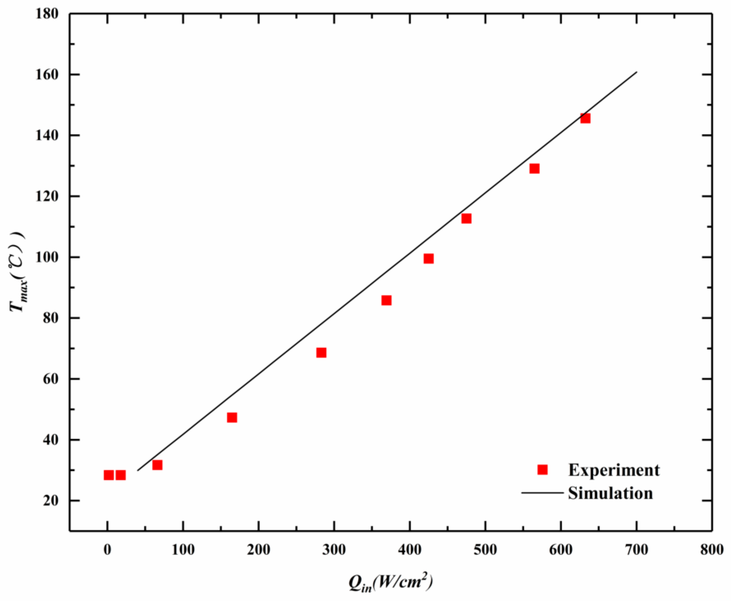
The 3D finite element models (FEMs) of the GaN power amplifier mounted on the PCB were constructed by Comsol Multiphysics software, as shown in Figure 1. To provide a heat flux in the chip, the 11 fingers were set as the heat source, which was set as the top surface of the GaN layer. In this model, the AlGaN barrier material was neglected, and the ambient temperature was set at 22 °C. Additionally, natural convection between the test module and air was taken into consideration, with a heat transfer coefficient (h) of 6 Wm−2 K−1. Moreover, tetrahedron elements were applied in our model for meshing.
The simulation results were compared with the experimental data extracted from the IR measurement at the finger of the GaN chip at different power densities, as displayed in Figure 4. According to the comparison results, the experimental results agreed well with the simulation results. Consequently, the 3D FEMs of the GaN power amplifier mounted on the bare silicon wafer and some traditional carrier materials of GaN chips (such as LTCC/HTCC) were constructed by the Comsol Multiphysics software using the same model. The material characteristics are listed in Table 2.
2.4. Data Reduction
Thermal resistance (θ) is defined as the ratio of temperature drop (ΔT) to the dissipated heat transfer rate (Pd):
Considering that a cooling system was introduced into the liquid loop and that the water temperature changed with junctions, the reference temperature was uniformly set as the ambient temperature (Tamb = 22 °C) during the experiments and thermal resistance calculation (not the inlet water temperature). Figure 5 demonstrates the thermal resistance model used to simplify the calculation and analysis of thermal management enhancement. The heating area was under the gate, as presented in Figure 5a. In this paper, the maximum temperature of the GaN chip was referred as Tj, measured by the IR system in junction area of the GaN chip. Tsink should be considered the average temperature of the area under the GaN power amplifier that could not be obtained in experiments. As the size of the GaN chip was much smaller than the mounting plates size (lateral heat conduction over a small distance can be ignored), Tsink was simplified and regarded as the average temperature of four points on the top surface of mounting plates that were adjacent to the edges of the chip.
As displayed in Figure 5, the equivalent thermal resistance circuit illustrated the thermal path from the power source to ambient air. The chip heating resource was the GaN region under the gate fingers. According to JESD51-1, when the heat sink was applied to dissipate the heat power of the chip, an accurate relationship of junction temperature, thermal resistance and dissipated power was expressed as:
where Tj is the junction temperature, Tamb stands for ambient temperature, Pd indicates the dissipated heat power, θja represents the thermal resistance of natural convection and radiation from the junction to the ambient thermal path, θsa represents the thermal resistance from the heat sink to ambient air (including processes of forced and natural convection and radiation) and θjs represents thermal resistance from the junction to the heat sink, which is a summation of the following:
Therefore, θtotal is defined as the following:
The IR system obtained the temperature distribution on the test module’s surface in the horizontal direction, but not the inner materials in the vertical direction; therefore, θGaN, θSiC and θAuSn could not be obtained from the experimental temperatures. In this regard, we would estimate these three resistances theoretically by absolute thermal resistances θt, which are properties of particular components (certain thermal conductivity k, as the influence of temperature was ignored) and defined geometries (thickness and area):
3. Results and Discussion
3.1. PCB, Bare Silicon Wafer and MPFHS
Figure 6 displays the variation of maximum temperature of the GaN-on-SiC power amplifier mounted on three different plates (PCB, bare silicon wafer and MPFHS) probed by the IR camera system that was focused on the devices at different power densities, presented by dot lines. Typically, the maximum temperature was referred to as the temperature of junction. During the experiments, the mass flow rates of the MPFHS were changed from 0 to 90 mL/min. Figure 6 also illustrates the compared thermal simulation results of the GaN device brazed to PCB, bare silicon wafer and LTCC/HTCC plates, presented by dash lines.
Generally, the device mounted on LTCC plate showed the worst performance, due to the extremely low thermal conductivity (as low as 2 Wm−1 K−1), much like a thermal isolator rather than a thermal conductor. The device could not dissipate heat effectively in the vertical direction. The total dissipated power density was under 200 W/cm2 and temperature had already achieved highs of up to 150 °C. GaN mounted on the PCB also performed badly, with a relatively low thermal conductivity of 9.5 Wm−1 K−1, and a very high temperature (145°C) achieved at a heat power density of lower than 640 W/cm2.
In this study, the maximum temperatures of GaN mounted on the bare silicon wafer and MPFHS with no convective liquid structure were almost the same. The increased surface area of MPFs made no difference in the heat transfer enhancement, because the BF33 borosilicate glass cover plate blocked the natural convection between MPFs and the air. Two test plates achieved 254.4% power density increments (up to 1700 W/cm2) compared to the PCB plate at the same junction temperature of 145 °C due to increasing material thermal conductivity. When the mounting material was changed to HTCC, thermal conductivity increased further to 180 Wm−1 K−1, and power density increased to 3500 W/cm2. Thus, a conclusion can be made that the thermal performance of a GaN device can be improved by increasing the thermal conductivity of the mounting material.
Moreover, by combining the MPFHS with a liquid loop, the power density range of the GaN power amplifier was significantly extended to reach 7250 W/cm2 at a Tj of 145 °C and a mass flow rate of 90 mL/min, which is nearly a four-fold increase compared to GaN mounted on the bare silicon wafer, and 11.5 times better relative to GaN mounted on the PCB. When compared with the traditional mounting plate material HTCC, the heat dissipation ability was enhanced two-fold.
On the other hand, the increasing mass flow rate also extended the power density range of the device from 6800 to 7257 W/cm2 at the Tj of 145 °C. However, the improvement by increasing flow rate was limited, with much effort remaining to be made on factors affecting the heat transfer performance of an MPFHS, such as the pin fins arrangement [13,14], surface roughness [15,16,17], surface hydrophilia/hydrophobicity [18,19,20] and surface coating with nanowire/nanoparticles [21,22,23], so as to attain a superior heat removal capacity.
3.2. Thermal Resistance Analysis
Table 3 summarizes the thermal resistance calculated from experimental data using Equations (1)–(4). Clearly, the thermal resistance decreased when the plate changed from the PCB to the bare silicon wafer, which is attributable to the higher thermal conductivity of silicon than PCB. In addition, the MPFHS without liquid cooling had a slightly higher thermal resistance than the bare silicon wafer. This might have been related to the fact that the air sandwiched between the silicon MPF and the glass cover plate (with a very low thermal conductivity of 1.005 Wm−1 K−1) blocked the direct heat exchange with ambient air. When GaN was mounted on the MPFHS, the thermal resistance remarkably decreased to 4.097 °C/W at the flow rate of 30 mL/min. A limited improvement on thermal resistance to 3.13 °C/W at 90 mL/min was attained as the mass flow rate increased. θtotal was improved 18.5-fold compared with the PCB.
The θjs (junction to sink) in all cases was smaller than the θja (junction to ambient air), suggesting that the chip heat was dissipated mainly through the mounting heat sink plates. Therefore, it is important to analyze heat path junction to the sink, and we focus on θjs in the following discussion. The theoretical thermal resistance of θjs obtained by Equation (5) was 0.6485 °C/W (θGaN +θSiC +θAuSn), which was regarded as the limit value. In our experiments, θjs was reduced from 16.92 to 3.63 °C/W, and was improved 3.6-fold compared to the PCB, which was further decreased to the limit value. Figure 7 shows the decreasing trend of θjs that approached 0.6485 °C/W. The one reason θjs reduction was temperature dependent on thermal conductivities for the GaN, SiC and AuSn layers was that the thermal conductivities of solid materials increased with decreasing temperature. The difference between the experimental and theoretical θjs values was mainly ascribed to the phonon scattering at the interface of different materials.
Moreover, it was obtained by Equation (5) that θAuSn for the die attach represented over 70% of the θjs. Beyond the scope of this article, such a result illustrates that a further development of the die attach method may reduce the limitation of θjs, for instance, a direct die attach to MPFs, coolants without interlayers and the interchip cooling strategy [24,25].
4. Conclusions
IR thermography measurements were employed in this study to probe the device temperature of a GaN power amplifier grown on the SiC substrates mounted on different plates, namely, a PCB, a bare silicon wafer and an Si-based MPFHS, within the range of operating power. Additionally, a series of experiments were conducted to evaluate the cooling capacities of these three plates. The effect of mass flow rate on the MPFHS device temperature was also examined. Further, the experimental results were compared with 3D FEM thermal simulation results. The following conclusions are drawn from the experiments:
- (1)
- The thermal performance of a GaN device can be improved by increasing the thermal conductivity of the mounting material. The dissipated power density of the GaN power amplifier was 200 W/cm2 when mounted on LTCC (thermal conductivity is 2 Wm−1 K−1). While mounted on HTCC (thermal conductivity increasing to 180 Wm−1 K−1), the power density increased 17.5-fold to 3500 W/cm2.
- (2)
- The thermal performance of a GaN device can be improved by applying a silicon-based micro-pin fin heat sink. When mounted on the MPFHS, the power density reached 7250 W/cm2 (at a Tj of 145 °C and a mass flow rate of 90 mL/min), which is nearly a two-fold increase compared with traditional mounting material HTCC. This means that using a silicon-based MPFHS can improve the reliability of the device and reduce the junction temperature effectively, making it a promising thermal management method.
- (3)
- The improvement of thermal management was limited for GaN mounted on the MPFHS, with a mass flow rate increase from 30 to 90 mL/min. Nonetheless, lots of heat sink optimization schemes could be further developed to achieve the optimal cooling effect, such as the cross-shape of micro-pin fins or the pin fin arrangement.
- (4)
- The θtotal was improved 18.5-fold compared with the PCB and MPFHS at a mass flow rate of 90 mL/min. These significant results can elongate the mean time to failure and ensure a more reliable operation of GaN devices.
- (5)
- Replacing the traditional base plates (PCB, silicon wafer and LTCC/HTCC) with an MPFHS plate can significantly reduce the θjs to approach the theoretical limitation value. In future studies, this is a promising and possible way of developing the die-attach method in order to improve thermal interface resistance for solving this bottleneck problem. Alternatively, removing interface layers and adopting an interchip cooling strategy are also the promising approaches.
Author Contributions
Conceptualization, T.K. and B.J.; methodology, T.K., Y.Y. and Y.J.; validation, T.K., Y.Y. and Y.J.; formal analysis, T.K.; investigation, T.K. and Y.Y.; resources, B.J. and Y.K.; data curation, T.K.; writing—original draft preparation, T.K.; writing—review and editing, Y.K. and B.J.; visualization, T.K.; supervision, Y.K. and B.J.; project administration, Y.K. and B.J. All authors have read and agreed to the published version of the manuscript.
Funding
This research received no external funding.
Acknowledgments
The research is supported by the Chinese Equipment Pre-research Field Foundation Key Project (Grant no.61409230703).
Conflicts of Interest
The authors declare no conflict of interest.
Nomenclature
| ΔT | Temperature Drop [°C] |
| c | Specific Heat [Jkg−1 K−1] |
| FEM | Finite Element Model |
| HTCC | High-Temperature Co-fired Ceramics |
| h | Heat Transfer Coefficient [Wm−2 K−1] |
| k | Thermal Conductivity [Wm−1 K−1] |
| LTCC | Low-Temperature Co-fired Ceramics |
| MPFHS | Micro Pin Fin Heat Sink |
| P | Power [W] |
| PA | Power Amplifier |
| PCB | Printed Circuit Board |
| Q | Power Density [W/cm2] |
| Greek symbols | |
| θ | Thermal Resistance [°C/W] |
| ρ | Density [kg/m3] |
| Subscripts | |
| amb | Ambient |
| d | Dissipated power density |
| in | Input |
| j | Junction |
| ja | Junction to Ambient Air |
| js | Junction to Sink |
| max | Maximum |
| sa | Sink to Ambient Air |
| sink | Heat Sink |
| total | Total Thermal Resistance |
References
- Pomeroy, J.; Bernardoni, M.; Sarua, A.; Manoi, A.; Dumka, D.C.; Fanning, D.M.; Kuball, M. Achieving the Best Thermal Performance for GaN-on-Diamond. In Proceedings of the 2013 IEEE Compound Semiconductor Integrated Circuit Symposium (CSICS), Monterey, CA, USA, 13–16 October 2013; pp. 1–4. [Google Scholar]
- Park, J.; Shin, M.W.; Lee, C. Thermal Modeling and Measurement of GaN-Based HFET Devices. IEEE Electron Device Lett. 2003, 24, 424–426. [Google Scholar] [CrossRef]
- Sarua, A.; Ji, H.; Kuball, M.; Uren, M.; Martin, T.; Hilton, K.; Balmer, R. Integrated micro-Raman/ Infrared Thermography Probe for Monitoring of Self-Heating in AlGaN/GaN Transistor Structures. IEEE Trans. Electron Devices 2006, 53, 2438–2447. [Google Scholar] [CrossRef]
- Tian, T.; Sun, X.; Gao, H.; Lu, S. Improved Thermal Management of Power Cells with Adding Cooling Path from Collector to Ground. Electron. Lett. 2019, 55, 513–515. [Google Scholar] [CrossRef]
- Samanta, K.K. PA Thermal Management and Packaging: Wideband PA and Packaging, History, and Recent Advances: Part 2. IEEE Microw. Mag. 2016, 17, 73–81. [Google Scholar] [CrossRef]
- Sarua, A.; Ji, H.; Hilton, K.P.; Wallis, D.J.; Uren, M.J.; Martin, T.; Kuball, M. Thermal Boundary Resistance Between GaN and Substrate in AlGaN/GaN Electronic Devices. IEEE Trans. Electron Devices 2007, 54, 3152–3158. [Google Scholar] [CrossRef]
- Kuball, M.; Rajasingam, S.; Sarua, A.; Uren, M.J.; Martin, T.J.; Hughes, B.T.; Hilton, K.P.; Balmer, R.S. Measurement of Temperature Distribution in Multifinger AlGaN/GaN Heterostructure Field-Effect Transistors Using Micro-Raman Spectroscopy. Appl. Phys. Lett. 2003, 82, 124–126. [Google Scholar] [CrossRef]
- Faqir, M.; Batten, T.; Mrotzek, T.; Knippscheer, S.; Massiot, M.; Buchta, M.; Blanck, H.; Rochette, S.; Vendier, O.; Kuball, M. Improved Thermal Management for Gan Power Electronics: Silver Diamond Composite Packages. Microelectron. Reliab. 2012, 52, 3022–3025. [Google Scholar] [CrossRef]
- GaN Power Amplifier Design Solutions. 2018. Available online: https://www.microwavejournal.com/articles/31075-gan-power-amplifier-design-solutions (accessed on 20 October 2020).
- Ma, A.; Wei, J.; Yuan, M.; Fang, J. Enhanced Flow Boiling Heat Transfer of FC-72 on Micro-Pin-Finned Surfaces. Int. J. Heat Mass Transf. 2009, 52, 2925–2931. [Google Scholar] [CrossRef]
- Krishnamurthy, S.; Peles, Y. Flow Boiling of Water in a Circular Staggered Micro-Pin Fin Heat Sink. Int. J. Heat Mass Transf. 2008, 51, 1349–1364. [Google Scholar] [CrossRef]
- Colthup, N.B.; Daly, L.H.; Wiberley, S.E. Introduction to Infrared and Raman Spectroscopy, 2nd ed.; Academy Press: New York, NY, USA, 1975; pp. 69–118. [Google Scholar]
- Lorenzini, D.; Green, C.; Sarvey, T.; Zhang, X.; Hu, Y.; Fedorov, A.G.; Bakir, M.S.; Joshi, Y. Embedded Single Phase Microfluidic Thermal Management for Non-Uniform Heating and Hotspots Using Microgaps with Variable Pin Fin Clustering. Int. J. Heat Mass Transf. 2016, 103, 1359–1370. [Google Scholar] [CrossRef]
- Shafeie, H.; Abouali, O.; Jafarpur, K.; Ahmadi, G. Numerical Study of Heat Transfer Performance of Single-Phase Heat Sinks with Micro Pin-Fin Structures. Appl. Therm. Eng. 2013, 58, 68–76. [Google Scholar] [CrossRef]
- Gregorčič, P.; Zupančič, M.; Golobič, I. Scalable Surface Microstructuring by a Fiber Laser for Controlled Nucleate Boiling Performance of High-and Low-Surface-Tension Fluids. Sci. Rep. 2018, 8, 7461. [Google Scholar] [CrossRef] [PubMed] [Green Version]
- Heo, K.Y.; Kihm, K.D.; Lee, J.S. Fabrication and Experiment of Micro-Pin-Finned Microchannels to Study Surface Roughness Effects on Convective Heat Transfer. J. Micromechanics Microengineering 2014, 24, 125025. [Google Scholar] [CrossRef]
- Alam, T.; Lee, P.; Yap, C.R. Effects of Surface Roughness on Flow Boiling in Silicon Microgap Heat Sinks. Int. J. Heat Mass Transf. 2013, 64, 28–41. [Google Scholar] [CrossRef]
- Chen, B.; Zhou, Z.; Shi, J.; Schafer, S.R.; Chen, C.-L. Flooded Two-Phase Flow Dynamics and Heat Transfer with Engineered Wettability on Microstructured Surfaces. J. Heat Transf. 2015, 137, 091021. [Google Scholar] [CrossRef] [Green Version]
- Shen, C.; Zhang, C.; Bao, Y.; Wang, X.; Liu, Y.; Ren, L. Experimental Investigation on Enhancement of Nucleate Pool Boiling Heat Transfer Using Hybrid Wetting Pillar Surface at Low Heat Fluxes. Int. J. Therm. Sci. 2018, 130, 47–58. [Google Scholar] [CrossRef]
- Li, Q.; Yu, Y.; Zhou, P.; Yan, H. Enhancement of Boiling Heat Transfer Using Hydrophilic-Hydrophobic Mixed Surfaces: A Lattice Boltzmann Study. Appl. Therm. Eng. 2018, 132, 490–499. [Google Scholar] [CrossRef]
- Kim, B.S.; Shin, S.; Lee, D.; Choi, G.; Lee, H.; Kim, K.M.; Cho, H.H. Stable and Uniform Heat Dissipation by Nucleate-Catalytic Nanowires for Boiling Heat Transfer. Int. J. Heat Mass Transf. 2014, 70, 23–32. [Google Scholar] [CrossRef]
- Kim, B.S.; Shin, S.; Shin, S.J.; Kim, K.M.; Cho, H.H. Control of Superhydrophilicity/Superhydrophobicity using Silicon Nanowires via Electroless Etching Method and Fluorine Carbon Coatings. Langmuir ACS J. Surf. Colloids 2011, 27, 10148–10156. [Google Scholar] [CrossRef]
- Dixit, P.; Lin, N.; Miao, J.; Wong, W.K.; Choon, T.K. Silicon Nanopillars Based 3D Stacked Microchannel Heat Sinks Concept for Enhanced Heat Dissipation Applications in MEMS Packaging. Sens. Actuators A Phys. 2008, 141, 685–694. [Google Scholar] [CrossRef]
- Bar-Cohen, A.; Maurer, J.J.; Felbinger, J.G. Darpa’s Intra/Interchip Enhanced Cooling (Icecool) Program. In Proceedings of the International Conference on Compound Semiconductor Manufacturing Technology, CS MANTECH, New Orleans, LA, USA, 13–16 May 2013; pp. 171–174. [Google Scholar]
- Bar-Cohen, A. Gen-3 Thermal Management Technology: Role of Microchannels and Nanostructures in an Embedded Cooling Paradigm. J. Nanotechnol. Eng. Med. 2013, 4, 020907. [Google Scholar] [CrossRef]
Figure 1.
(a) Three-dimensional model of a GaN power amplifier mounted onto plates (not to scale), (b) Cross-sectional view of the GaN chip with integrated MPFHS (micro-pin fin heat sink) (not to scale).
Figure 1.
(a) Three-dimensional model of a GaN power amplifier mounted onto plates (not to scale), (b) Cross-sectional view of the GaN chip with integrated MPFHS (micro-pin fin heat sink) (not to scale).

Figure 2.
Si-based MPFHS: (a) schematic diagram of MPFHS; (b) microscopic image of an MPF (micro-pin fins).
Figure 2.
Si-based MPFHS: (a) schematic diagram of MPFHS; (b) microscopic image of an MPF (micro-pin fins).

Figure 3.
(a) Close-loop of the experimental test platform; (b) an IR camera was focused on the GaN power amplifier chips area (off working state).
Figure 3.
(a) Close-loop of the experimental test platform; (b) an IR camera was focused on the GaN power amplifier chips area (off working state).
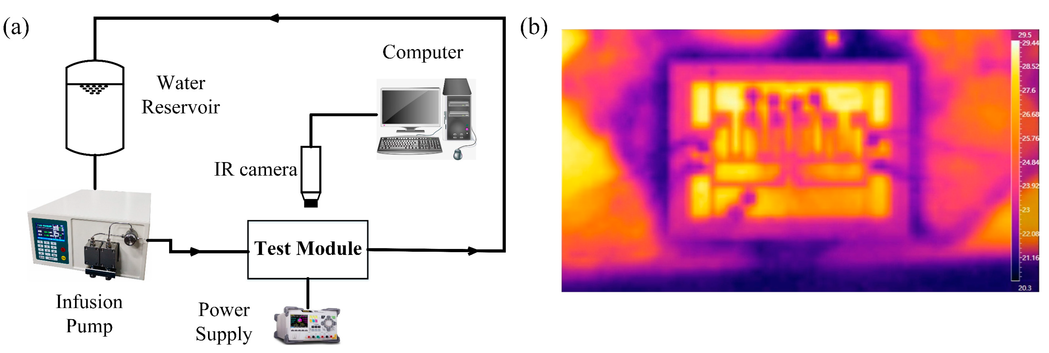
Figure 4.
Maximum temperature of GaN chips (mounted on PCB) as a function of input power density obtained based on IR measurements and 3D FEM (finite element models) simulation results.
Figure 4.
Maximum temperature of GaN chips (mounted on PCB) as a function of input power density obtained based on IR measurements and 3D FEM (finite element models) simulation results.

Figure 5.
Thermal resistance model: (a) material system for the test module; (b) thermal resistance circuit for calculation and analysis.
Figure 5.
Thermal resistance model: (a) material system for the test module; (b) thermal resistance circuit for calculation and analysis.
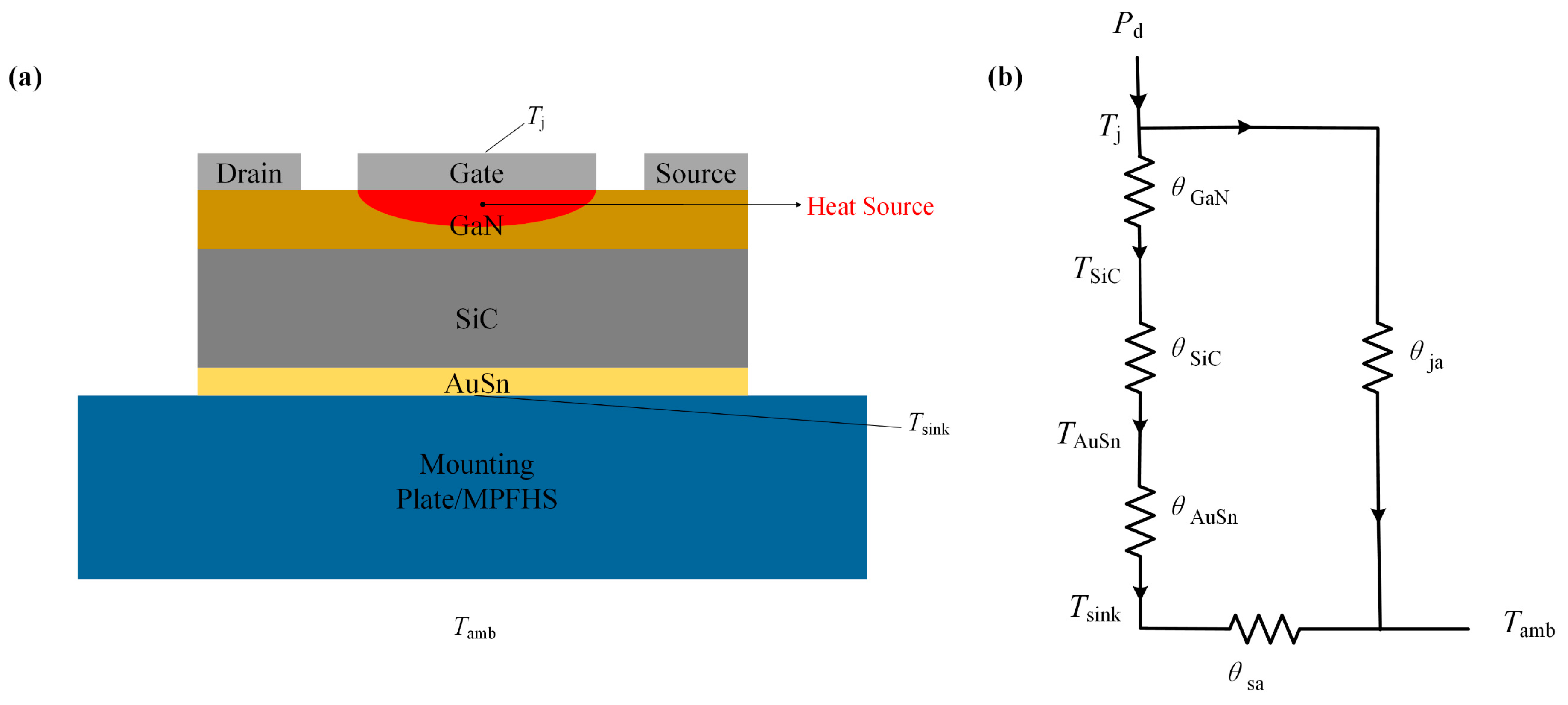
Figure 6.
The maximum temperature of the GaN power amplifier mounted on three different plates (PCB, bare silicon wafer and MPFHS) as a function of dissipated power density probed by the IR camera system. During the experiments, the mass flow rates of the MPFHS were changed from 0 to 90 mL/min.
Figure 6.
The maximum temperature of the GaN power amplifier mounted on three different plates (PCB, bare silicon wafer and MPFHS) as a function of dissipated power density probed by the IR camera system. During the experiments, the mass flow rates of the MPFHS were changed from 0 to 90 mL/min.
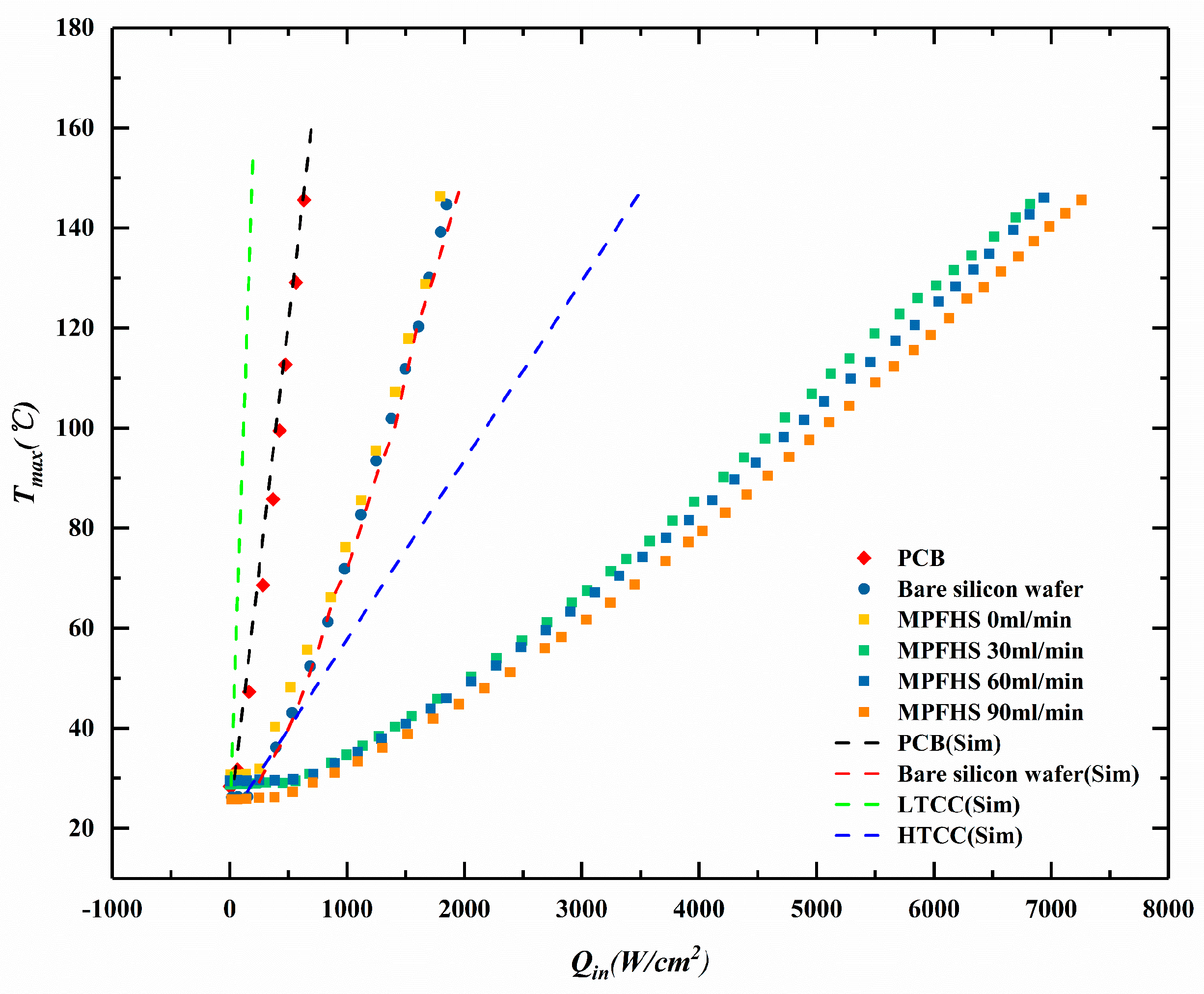
Figure 7.
Decreasing trend of θjs and the theoretical limitation of 0.6458 °C/W


Table 1.
Parameters of the equipment.
| Parameters | GaN PA | PCB (Printed Circuit Board) | Bare Silicon Wafer | MPFHS |
|---|---|---|---|---|
| Length | 1100 μm | 2 cm | 2 cm | 2 cm |
| Width | 800 μm | 2 cm | 2 cm | 2 cm |
Table 2.
Characteristics of materials in thermal simulation.
| Materials | Thermal Conductivity [Wm−1 K−1] | Specific Heat [Jkg−1 K−1] | ρ [kg m−3] | Thickness [μm] | Area [mm2] |
| GaN | 150 | 490 | 6070 | 2 | 1.1 × 0.8 |
| SiC | 420 | 690 | 3216 | 50 | 1.1 × 0.8 |
| AuSn | 57 | 150 | 14,700 | 25 | 1.1 × 0.8 |
| LTCC | 2 | 900 | 2500 | 500 | 20 × 20 |
| PCB | 9.5 | 1369 | 1900 | 500 | 20 × 20 |
| Si | 150 | 700 | 2329 | 500 | 20 × 20 |
| HTCC | 180 | 750 | 3280 | 500 | 20 × 20 |
Table 3.
Thermal resistance calculated from experimental data at the same power dissipation.
| Dissipated Heat Power (W) | θja (°C W−1) | θjs (°C W−1) | θsa (°C W−1) | θtotal (°C W−1) | |
|---|---|---|---|---|---|
| PCB | 1.012 | 122.13 | 16.92 | 105.22 | 61.07 |
| Bare silicon wafer | 1.068 | 28.46 | 8.61 | 19.85 | 14.237 |
| MPFHS (0 mL/min) | 1.059 | 31.82 | 9.93 | 21.90 | 15.917 |
| MPFHS (30 mL/min) | 1.087 | 8.188 | 4.02 | 4.17 | 4.097 |
| MPFHS (60 mL/min) | 1.133 | 7.81 | 3.83 | 3.99 | 3.91 |
| MPFHS (90 mL/min) | 1.139 | 6.27 | 3.63 | 2.63 | 3.13 |
Publisher’s Note: MDPI stays neutral with regard to jurisdictional claims in published maps and institutional affiliations. |
© 2020 by the authors. Licensee MDPI, Basel, Switzerland. This article is an open access article distributed under the terms and conditions of the Creative Commons Attribution (CC BY) license (http://creativecommons.org/licenses/by/4.0/).
Share and Cite
MDPI and ACS Style
Kang, T.; Ye, Y.; Jia, Y.; Kong, Y.; Jiao, B. Enhanced Thermal Management of GaN Power Amplifier Electronics with Micro-Pin Fin Heat Sinks. Electronics 2020, 9, 1778. https://doi.org/10.3390/electronics9111778
AMA Style
Kang T, Ye Y, Jia Y, Kong Y, Jiao B. Enhanced Thermal Management of GaN Power Amplifier Electronics with Micro-Pin Fin Heat Sinks. Electronics. 2020; 9(11):1778. https://doi.org/10.3390/electronics9111778
Chicago/Turabian StyleKang, Ting, Yuxin Ye, Yuncong Jia, Yanmei Kong, and Binbin Jiao. 2020. "Enhanced Thermal Management of GaN Power Amplifier Electronics with Micro-Pin Fin Heat Sinks" Electronics 9, no. 11: 1778. https://doi.org/10.3390/electronics9111778
Note that from the first issue of 2016, this journal uses article numbers instead of page numbers. See further details here.