Hot Carrier Stress Sensing Bulk Current for 28 nm Stacked High-k nMOSFETs
by
 ,
,
Chii-Wen Chen
1, 
Mu-Chun Wang
1,*,
Cheng-Hsun-Tony Chang
1,
Wei-Lun Chu
1,
Shun-Ping Sung
2 and
Wen-How Lan
3,* 1
Department of Electronic Engineering, Minghsin University of Science and Technology, Hsinchu 30401, Taiwan
2
Graduate Institute of Mechatronic Engineering, National Taipei University of Technology, Taipei 10608, Taiwan
3
Department of Electrical Engineering, National University of Kaohsiung, Kaohsiung 81148, Taiwan
*
Authors to whom correspondence should be addressed.
Electronics 2020, 9(12), 2095; https://doi.org/10.3390/electronics9122095
Submission received: 23 October 2020
/
Revised: 27 November 2020
/
Accepted: 4 December 2020
/
Published: 8 December 2020
(This article belongs to the Special Issue Application of Electronic Devices on Intelligent System)
Abstract
:This work primarily focuses on the degradation degree of bulk current (IB) for 28 nm stacked high-k (HK) n-channel metal–oxide–semiconductor field-effect transistors (MOSFETs), sensed and stressed with the channel-hot-carrier test and the drain-avalanche-hot-carrier test, and uses a lifetime model to extract the lifetime of the tested devices. The results show that when IB reaches its maximum, the ratio of VGS/VDS values at this point, in the meanwhile, gradually increases in the tested devices from the long-channel to the short ones, not just located at one-third to one half. The possible ratiocination is due to the ON-current (IDS), in which the short-channel devices provide larger IDS impacting the drain junction and generating more hole carriers at the surface channel near the drain site. In addition, the decrease in IB after hot-carrier stress is not only the increment in threshold voltage VT inducing the decrease in IDS, but also the increment in the recombination rate due to the mechanism of diffusion current. Ultimately, the device lifetime uses Berkley’s model to extract the slope parameter m of the lifetime model. Previous studies have reported m-values ranging from 2.9 to 3.3, but in this case, approximately 1.1. This possibly means that the critical energy of the generated interface state becomes smaller, as is the barrier height of the HK dielectric to the conventional silicon dioxide as the gate oxide.
Keywords:
drain current; hot-carrier; impact ionization; high-k; lifetime; substrate current; ALD technology1. Introduction
With the continuous scaling of complementary metal–oxide–semiconductor (CMOS) technology, there are many benefits to metal–oxide–semiconductor field-effect transistors (MOSFETs), including an increasing number of devices in integrated circuits, not only providing impressive electrical performance of the device, but also decreasing the entire power consumption. However, the shorter channel length and thinner gate dielectric thickness of the MOSFET increase the OFF-current including the gate leakage and source/drain (S/D) punch-through effect, and relatively influencing the threshold voltage (VT), short channel effect, and reliability issues [1,2]. In terms of reliability, the device lifetime will be reduced by hot carrier injection (HCI) [3,4]. The most common physical model for HCI is the lucky carry model built by Hu et al. [5]. Berkeley’s model can derive the device lifetime with bulk current (or called substrate current (ISUB)). The model is shown in Equation (1).
where τ is the device lifetime, IDS is the drain-to-source current, ISUB is the substrate current, and the acceleration factor m = ϕit/ϕi, where ϕit is the critical hot carrier energy required to create an interface state of approximately 3.7 eV and ϕi is the minimum hot carrier energy required to create an impact ionization of approximately 1.3 eV for the poly-gate and Si-SiO2 interface.
The hot carrier effect can be classified into two types: Channel-hot-carrier (CHC) and drain-avalanche-hot carrier (DAHC) tests [6]. The CHC effect means that the carriers near the drain terminal are accelerated by the lateral electric field and travel through the channel [7,8,9,10,11,12], as shown in Figure 1. The quoted references related to hot-carrier (HC) effects are listed in Table 1. Studies have shown that the maximum ISUB (ISUB_max) is at VDS = VGS [13,14]. As VDS > VGS, the depletion region near the drain site is increased. As the carriers in the channel travel through this region, they are accelerated and energized to become hot carriers. These hot carriers may generate extra electron–hole pairs [15] in the channel, especially in the depletion region of the drain size. This phenomenon is called impact ionization. The generated electron may inject into the gate or drain terminal, and the generated holes trend to the substrate, as shown in Figure 2. The results demonstrate that the ISUB_max value is located at VGS = VDS/3 ~ VDS/2 [16,17], called the DAHC effect.
In particular, while the thickness of the silicon dioxide (SiO2)-based gate dielectric approaching its physical limitation, at the 45 nm-node-technology generation [18,19,20], is below 15 Å, gate leakage due to the direct tunneling effect cannot be tolerated at the OFF-current specification. Using the stacked high-k (HK) dielectric (HfOx/ZrOy/HfOz (HZH)), replacing the conventional SiO2 in gate engineering or halo implants and lightly doped-drain (LDD) technology in the surface channel is a couple of attractive metrologies to promote the drive current and decrease the leakage in nano-node process technology [21].
In this study, we used a HK-stack and metal gate (MG) as the n-MOSFET structure to analyze the variation in substrate current under hot carrier stresses [22]. In Equation (1), the severity of hot carrier injection is observed by the degradation in the substrate current, related to the issues of device lifetime. The other interesting event is to expose the relationship between channel lengths and substrate currents in nano-node n-MOSFETs. In addition, we used different stress conditions to probe the impact of substrate current, and investigated the τ × IDS/W vs. The ISUB/IDS model extracts the slope parameter m in Equation (1). In this study, VT extraction was followed the constant current methodology. To accelerate the process and circuit development in yield and reliability analysis in the nano-node era, the technology computer-aided design simulator is an appropriate choice as an assistant [23,24,25].
2. Concise Process Flow and Stress Conditions
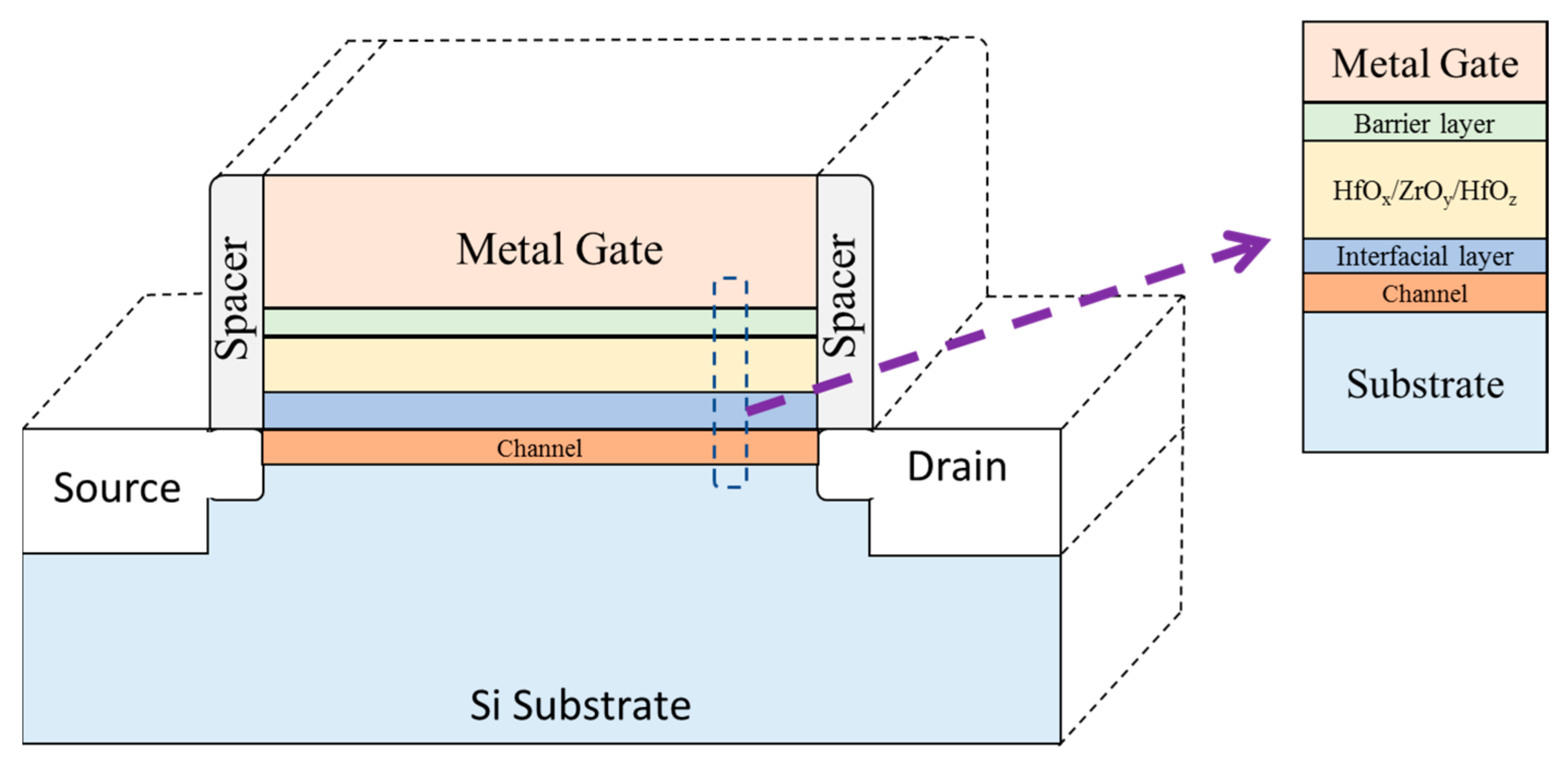
In this study, the schematic tested devices on 28 nm HK/MG wafers fabricated from the United Microelectronics Corporation (UMC) are used to perform the related extraction and analysis, as shown in Figure 3. After the standard cleaning, an interfacial layer (IL) of SiOx of approximately 9 Å was grown thermally to play a buffer between the surface channel and HK material and resist the nitrogen free radical to arrive at the surface channel to form the silicon nitride. Subsequently, the HK material was deposited as HZH by atomic layer deposition (ALD) technology [26,27,28]. In sequence, the devices were processed with the decoupled plasma nitridation (DPN) treatment to retard the amount of oxygen vacancies [29,30]. The treatment process employed the annealing temperature (700 °C) and nitrogen concentration (8%) after accomplishing an HK layer. The other key processes include an Si-based substrate, channel implantation, S/D engineering, interfacial layer, barrier metal, and low-resistivity Al metal gate. The metal gate was adopted in the gate-last (GL) process technology [31]. This technology provides several good functions to reduce the threshold voltage, gate electrode resistance, power consumption, and gate delay. The detailed 28 nm HK/MG process flow with the GL process can be referred to Wang et al. [21].
The basic electrical characteristics and stress tests were performed using a Keithley 4200 Semiconductor Characterization System. The test conditions can be divided into two parts. The first part is that the ISUB is measured with different channel lengths to observe the impact of the channel length change. The measurement conditions are listed in Table 2. The second part is related to the measurement of the HC degradation test. In these stresses, different stress voltages and channel lengths were applied to sense and analyze the most serious stress method, either CHC or DAHC stress [32]. The measurement conditions are presented in Table 3 with the VT extraction metrology following the constant current measurement.
3. Results and Discussion
3.1. The Relationship between the Channel Length and ISUB
The ISUB–VGS curves of n-MOSFETs were measured for different channel lengths, as shown in Figure 4. When the tested device was in the OFF state, the increment in absolute value of gate voltage at the negative VGS axis increased the ISUB because of the gate-induced drain leakage effect [33]. However, as the tested device was operated in the ON state, the gate voltage increased, inducing an increment in ISUB. This effect points to the fact that the average carriers in short channels are hotter and have more energy to create an impact ionization event. Thus, the rate of increase in ISUB with the shorter channel-length device is higher than the increase in IDS. As the channel length of the tested device decreases, the lateral electric field increased, and the IDS increases, resulting in an impact ionization rate (ISUB/IS), where IS is the current sensed at the source terminal, which increases, as shown in Figure 4a. While the channel length decreased, the maximum ISUB with the increase in VGS increases, generating a higher impact ionization rate, as shown in Figure 4b. The possible ratiocination indicates that the gate voltage increases, indicating a stronger vertical field, to attract more inversion electrons to recombine the holes in the longer channel length.
3.2. ISUB and VT Degradation after HC Stresses
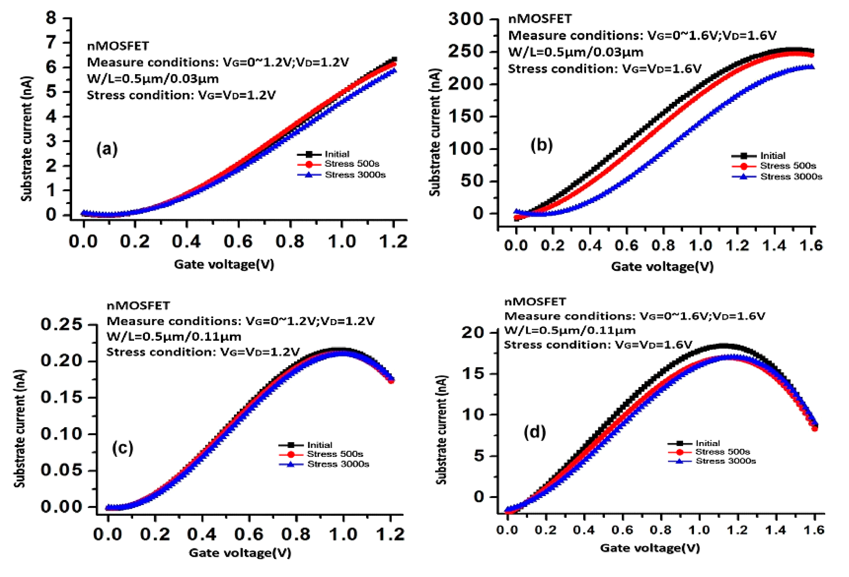
The stress conditions in the CHC stress mode are listed in Table 3. Figure 5 illustrates that the short channel device causes serious degradation owing to the larger horizontal field from the drain site to the source node, and the higher stress voltage can also increase the device degradation in the ISUB aspect. In summary, the most obvious degradation for ISUB is set at the tested device W/L = 0.5/0.03 µm and the stress voltage at VGS = VDS = 1.6 V. The other degradation index VT shifts with different channel lengths, and the different stress voltages are shown in Figure 6. The VT shift observed at L = 0.03 µm and the stress voltage VGS = VDS = 1.6 V are the worst [34,35,36]. However, as the stress condition is at the higher gate field, the distribution of VT shift at L = 0.03 µm and 0.11 µm is similar, as shown in Figure 6b,d, but not at the lower field, as shown in Figure 6a,c. This speculation is that the capability of trap repair in the lower field is better in the channel, and so is the longer device. Following the research results of Huang et al. [37], they denoted that the drain current in the nano-MOSFETs covers the drift and diffusion currents, fitting well in simulation and measured electrical current–voltage characteristics. In this reference, the carrier conduction in the channel is similar to that in a p-n junction. The entire current flow in the p-n junction is mainly dominated by the diffusion mechanism. Therefore, a reasonable speculation of the decrement in ISUB after HC stress is not only the increase in VT indirectly causing the decrease in IDS, but also the increase in the recombination rate arising from the diffusion current, especially for the nano-node devices. As the channel length is less than 0.04 μm, this consequence is more distinct regardless of the HC stress method.
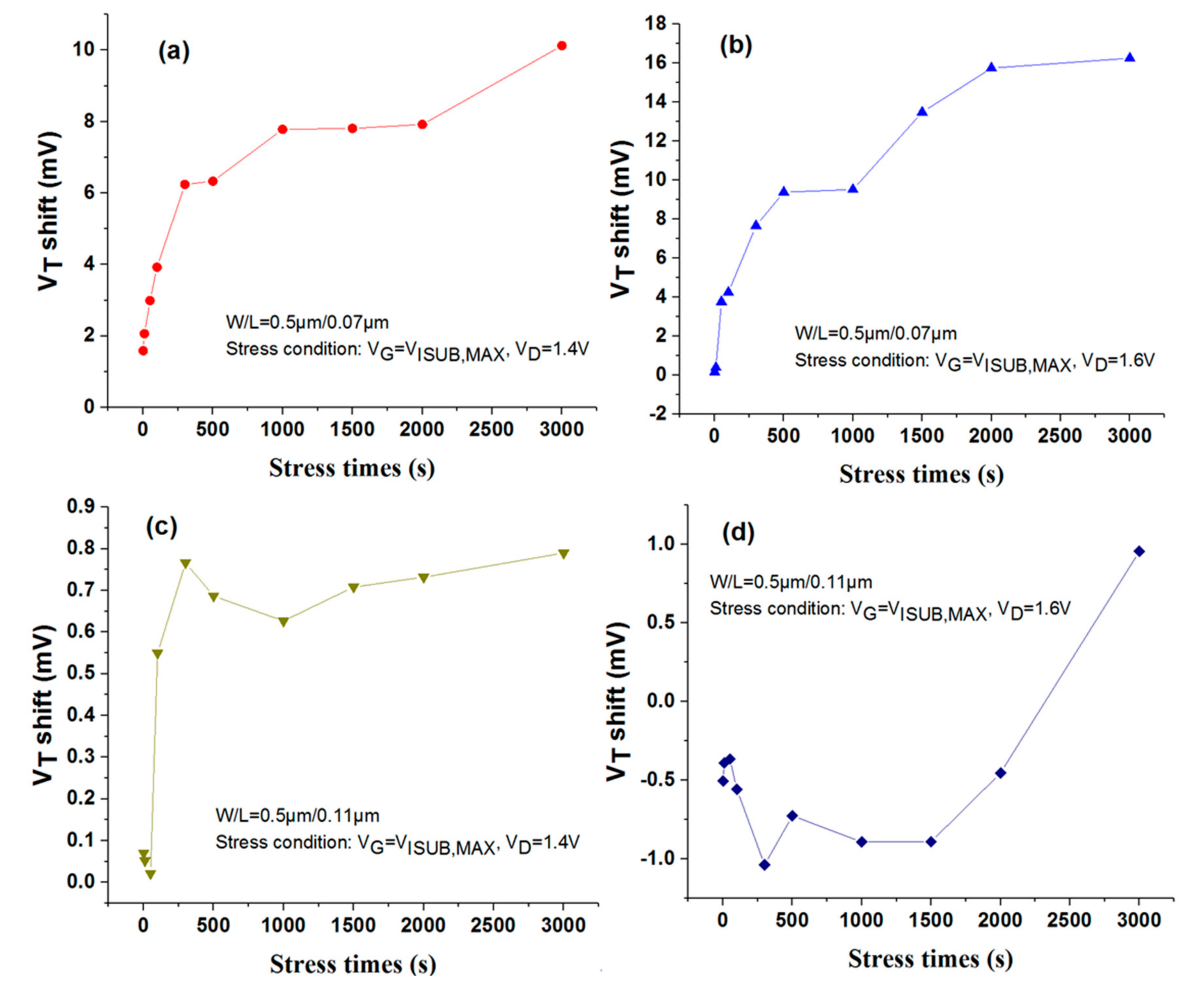
In the DAHC stress mode, the stress conditions are similar to the CHC stress. The slight difference is that the gate voltage is defined by the VGS at the maximum ISUB. The test results show that the maximum ISUB does not appear in the short-channel device (L = 0.03 µm). Therefore, the discussion will only focus on the tested devices with L = 0.07 µm and L = 0.11 µm. Figure 7 shows that the most serious degradation of ISUB is at L = 0.07 µm and the stress voltage VDS = 1.6 V. The VT shift is shown in Figure 8. The worst degradation is at L = 0.07 µm and the stress voltage VGS at ISUB_max and VDS = 1.6 V. After the DAHC stress, the substrate current is similarly decreased by the increase in VT, causing a decrease in IDS and an increase in the recombination rate from the diffusion current.
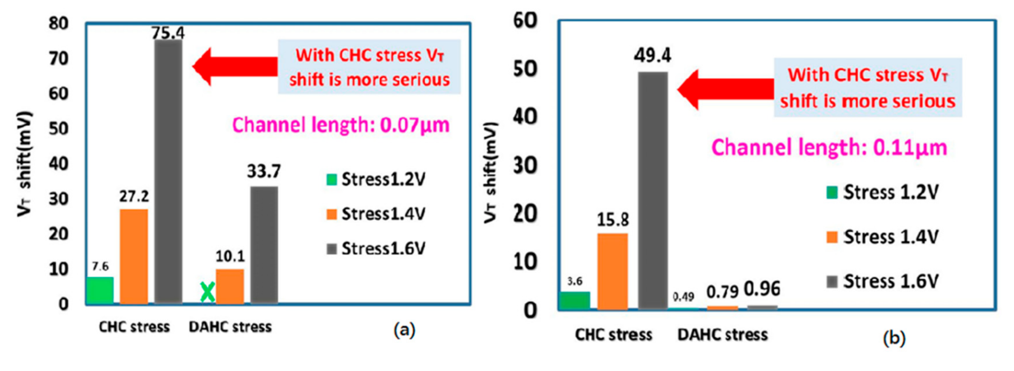
By observing the amount of VT shift with CHC and DAHC tests, the value of VT-shift with the CHC test is higher than that with the DAHC test. This phenomenon is similar to that reported in [32]. As deep analysis, because of the low gate field, the distribution trends of VT shift vs. stress time are not the same, which are different from the consequences under the CHC stress. However, the decrease trends of substrate current both before and after the HC stresses seem compatible.
3.3. HC Lifetime Model for n-MOSFETs
The τ × IDS/W vs. ISUB/IDS model [5,16] is adopted into these tested devices, as in Equation (1). The model can effectively explain the correlation between ISUB and lifetime (τ). When the ISUB increases, the lifetime decreases. This indicates that when the ISUB is larger, the HC effect and the device degradation become serious. The slope of the predicted line, m, is 1.1, as shown in Figure 9, compared with the former research m ranging from 2.9 to 3.3 for SiO2. The decrement in m-value means that the interface states become easier to generate due to the HK structure. According to references [38,39], the work function of polygrain Al is 4.13 eV and the band offset of HfO2 compared to Si is 1.5 eV. The affinity of Si is 4.05 V. The barrier height between gate Al and HfO2 is approximately 1.58 eV, close to the critical hot carrier energy, requiring the creation of an interface state ϕit, as shown in Figure 10. If we adopt the ϕi = 1.3 eV minimum hot carrier energy to create an impact ionization in the Si-based surface channel, the ratio of ϕit/ϕi representing the theoretical m-value is approximately 1.2, which is very close to the extracted m parameter 1.1.
After stress, the subthreshold swing SS is changed, related to the change in interface integrity between the IL and Si-based channel. The ∆SS (SS value after stress—SS value before stress) is equal to
where k is Boltzmann’s constant, T is the absolute temperature, q is the unit charge, Cit is the equivalent interface-state capacitance per area = qDit, Dit is the interface state density, Nit is the interface state number per area with integration of Dit in the energy band, and Cox is the gate capacitance per area.
The threshold voltage change, ∆VT, after stress contains the change in the oxide trap in the gate dielectric and the interface state on the surface channel, as shown in Equation (3). ∆Qf covers the qNit change q∆Nit and qNot change q∆Not, where Not is the oxide trap number per area in the gate dielectric.
Using Equations (2) and (3), ∆Nit and ∆Not can be decoupled after hot carrier stress. These two amounts also explain the degradation level of the oxide trap and interface trap state for a tested device under a long-time operation, as shown in Figure 11 with W/L = 1/0.03 µm under different plasma nitridation treatments [21,39,40]. ∆Nit or ∆Not with different nitridation treatments exposes the different historical trends in hot carrier stress. In addition, in terms of the test consequences, the VT-shift with CHC stress is more serious than that with DAHC, as shown in Figure 12. Even though the observed ISUB_max occurs well under DAHC stress conditions, the major degradation mechanism still comes from the interface state and/or oxide trap generation [41,42,43,44]. Moreover, the generation of the interface state near the IL is also possibly due to the channels strained, which could be more relevant to reduce the bonding energy than that on the top of the HK layer. Due to the CHC stress mode owing to the higher gate voltage generating more interface states and oxide traps, the VT-shift in the worst case under the view of ISUB_max can be effectively demonstrated to be attributed to the VGS = VDS stress condition, not at VGS traditionally located at one-third to one-half VDS [5].
4. Conclusions
In this work, we observe that the maximum substrate current and the ratio of ISUB/Is before the HC stress increased as the channel length of the tested devices was shorter. After the HC stress, the ISUB_max decreased, especially for the deep nano-node channel-length device because of the increase in VT indirectly degrading the IDS and the increase in the recombination rate from the diffusion current as the channel length entered the nano-node level. Through the longer stress time, this phenomenon was more obvious, which also contributed to the VT shift. Even though the observed ISUB_max occurred well under DAHC stress conditions, the major degradation mechanism still came from the interface state and/or oxide trap generation. The other consistent agreement was to extract the HC lifetime with Berkley’s model, still available in HK/MG n-MOSFETs, deposited with ALD technology, but the values of acceleration factor m were different from the gate dioxide or oxy-nitride. Ultimately, the HC stress is indeed and still a good gauge or application in nano-node device reliability tests or process splits in the optimal adjustment of front-end processes, such as channel implementation, growth of the gate dielectric, or HK dielectric deposition with nitridation treatment.
Author Contributions
Conceptualization, C.-W.C.; methodology, W.-H.L. and S.-P.S.; formal analysis, C.-W.C. and M.-C.W.; data curation, S.-P.S. and W.-L.C.; writing—Original draft preparation, M.W.; writing—Review and editing, M.-C.W.; project administration, C.-H.-T.C. All authors have read and agreed to the published version of the manuscript.
Funding
This research received no external funding.
Acknowledgments
The authors cordially thank United Microelectronics Corporation in Taiwan for providing precious 12” wafers, and the financial support from Ministry of Science and Technology of Republic of China under Contract Nos. MOST 109-2622-E-159-001.
Conflicts of Interest
The authors declare no conflict of interest.
Abbreviations
| Tox | Thickness of oxide |
| CADDET | Computer-Aided Device Design in Two Dimensions |
| R-D | Recombination-Diffusion |
| SDE | Source/Drain Extension |
| LEM | Lucky Electron Model |
| BTI | Bias Temperature Instability |
| EOT | Equivalent Oxide Thickness |
References
- Taur, Y.; Ning, T.H. CMOS Performance Factors. In Fundamentals of Modern VLSI Devices; University Press: Cambridge, UK, 2018; pp. 256–317. [Google Scholar]
- Pearce, C.W.; Yaney, D.S. Short-channel effects in MOSFET’s. IEEE Electron Dev. Lett. 1985, 6, 326–328. [Google Scholar] [CrossRef]
- Childs, P.; Leung, C. New mechanism of hot carrier generation in very short channel MOSFETs. Electron. Lett. 1995, 31, 139–141. [Google Scholar] [CrossRef]
- Joly, Y.; Lopez, L.; Portal, J.M.; Aziza, H.; Ogier, J.L.; Bert, Y.; Julien, F.; Fornara, P. Matching degradation of threshold voltage and gate voltage of NMOSFET after Hot Carrier Injection stress. Microelectron. Reliab. 2011, 51, 1561–1563. [Google Scholar] [CrossRef]
- Tam, S.; Ko, P.K.; Hu, C. Lucky-electron model of channel hot-electron injection in MOSFET’s. IEEE Trans. Electron Dev. 1984, 31, 1116–1125. [Google Scholar]
- Takeda, E. Hot-carrier effects in scaled MOS devices. Microelectron. Reliab. 1993, 33, 1687–1711. [Google Scholar] [CrossRef]
- Yu, B.; Wann, C.H.J.; Nowak, E.D.; Noda, K.; Hu, C. Short-channel effect improved by lateral channel-engineering in deep-submicronmeter MOSFET’s. IEEE Trans. Electron Dev. 1997, 44, 627–634. [Google Scholar]
- Takeda, E.; Nakagome, Y.; Kume, H.; Asai, S. New hot-carrier injection and device degradation in submicron MOSFETs. IEEE Proc. I Solid State Electron Devices 1983, 130, 144. [Google Scholar] [CrossRef]
- Abramo, A.; Fiegna, C.; Venturi, F. Hot Carrier Effects in Short MOSFETs at Low Applied Voltages; Institute of Electrical and Electronics Engineers (IEEE): Piscataway, NJ, USA, 2002. [Google Scholar]
- la Rosa, G.; Rauch, S.E. Channel hot carrier effects in n-MOSFET devices of advanced submicron CMOS technologies. Microelectron. Reliab. 2007, 47, 552–558. [Google Scholar] [CrossRef]
- Mahapatra, S.; Sharma, U. A Review of Hot Carrier Degradation in n-Channel MOSFETs—Part I: Physical Mechanism. IEEE Trans. Electron Devices 2020, 67, 2660–2671. [Google Scholar] [CrossRef]
- Mahapatra, S.; Sharma, U. A Review of Hot Carrier Degradation in n-Channel MOSFETs—Part II: Technology Scaling. IEEE Trans. Electron Devices 2020, 67, 2672–2681. [Google Scholar] [CrossRef]
- Amat, E.; Kauerauf, T.; Degraeve, R.; de Keersgieter, A.; Rodriguez, R.; Nafria, M.; Aymerich, X.; Groeseneken, G. Channel Hot-Carrier Degradation in Short-Channel Transistors With High- kk/Metal Gate Stacks. IEEE Trans. Device Mater. Reliab. 2009, 9, 425–430. [Google Scholar] [CrossRef]
- Pagey, M.P. Hot-carrier reliability simulation in aggressively scaled MOS transistors. Ph.D. Thesis, Vanderbilt University, Nashville, TN, USA, 2003. [Google Scholar]
- Hofmann, K.R.; Werner, C.; Weber, W.; Dorda, G. Hot-electron and hole-emission effects in short n-channel MOSFET’s. IEEE Trans. Electron Dev. 1985, 32, 691–699. [Google Scholar] [CrossRef]
- Koike, N.; Tatsuuma, K. A Drain Avalanche Hot Carrier Lifetime Model for n- and p-Channel MOSFETs. IEEE Trans. Device Mater. Reliab. 2004, 4, 457–466. [Google Scholar] [CrossRef]
- Acovic, A.; la Rosa, G.; Sun, Y.C. A review of hot-carrier degradation mechanisms in MOSFETs. Microelectron. Reliab. 1996, 36, 845–869. [Google Scholar] [CrossRef]
- Kim, H.D.; Roh, Y.; Lee, J.E. Characteristics of high-k gate dielectric formed by the oxidation of sputtered Hf/Zr/Hf thin films on the Si substrate. J. Vac. Sci. Tech. 2004, 22, 1342–1346. [Google Scholar] [CrossRef]
- Wong, H. The Current Conduction Issues in High-k Gate Dielectrics; Institute of Electrical and Electronics Engineers (IEEE): Piscataway, NJ, USA, 2007; pp. 31–36. [Google Scholar]
- Wong, H.; Iwai, H. On the scaling issues and high-k replacement of ultrathin gate dielectrics for nanoscale MOS transistors. Microelectron Eng. 2006, 83, 1867–1904. [Google Scholar] [CrossRef]
- Wang, S.J.; Sung, S.P.; Wang, M.C.; Huang, H.S.; Chen, S.Y.; Fan, S.K.; Wang, S.J.; Sung, S.P.; Wang, M.C.; Huang, H.S.; et al. Electrical stress probing recovery efficiency of 28 nm HK/MG nMOSFETs using decoupled plasma nitridation treatment. Vacuum 2018, 153, 117–121. [Google Scholar] [CrossRef]
- Amat, E.; Kauerauf, T.; Rodriguez, R.; Nafria, M.; Aymerich, X.; Degraeve, R.; Groeseneken, G. A comprehensive study of channel hot-carrier degradation in short channel MOSFETs with high-k dielectrics. Microelectron. Eng. 2013, 103, 144–149. [Google Scholar] [CrossRef]
- Pfäffli, P.; Tikhomirov, P.; Xu, X.; Avci, I.; Oh, Y.S.; Balasingam, P.; Krishnamoorthy, S.; Ma, T.; Avcı, I. TCAD for reliability. Microelectron. Reliab. 2012, 52, 1761–1768. [Google Scholar] [CrossRef]
- Macaleoni, A.; Villa, C.M.; Medda, M. Emerging challenges for a built-in reliability in innovative Automotive ICs. In Proceedings of the ESREF 2018, Aalborg, Denmark, 1–5 October 2018. [Google Scholar]
- Han, C.; Shi, X.; Huang, Q. Optimization of short channel effect and external resistance on small size FinFET for different threshold voltage flavors and supply voltages. Microelectron. J. 2019, 85, 1–5. [Google Scholar] [CrossRef]
- Tsai, C.H.; Yang, C.W.; Hsu, C.H.; Lai, C.M.; Lo, K.Y.; Chen, C.G.; Huang, R.M.; Tsai, C.T.; Hung, L.S.; You, J.W.; et al. Characteristics of HfZrOx Gate Stack Engineering forR Improvement on 28nm HK/MG CMOS Technology; Institute of Electrical and Electronics Engineers (IEEE): Piscataway, NJ, USA, 2012; pp. 1–2. [Google Scholar]
- Hegde, R.I.; Triyoso, D.H.; Samavedam, S.B.; White, B.E. Hafnium zirconate gate dielectric for advanced gate stack applications. J. Appl. Phys. 2007, 101, 74113. [Google Scholar] [CrossRef]
- Chung, S.; Yeh, C.H.; Feng, H.J.; Lai, C.S.; Yang, J.J.; Chen, C.C.; Jin, Y.; Chen, S.; Liang, M.-S. Impact of STI on the Reliability of Narrow-Width pMOSFETs With Advanced ALD N/O Gate Stack. IEEE Trans. Device Mater. Reliab. 2006, 6, 95–101. [Google Scholar] [CrossRef]
- Chiang, C.K.; Chang, J.C.; Liu, W.H.; Liu, C.C.; Lin, J.F.; Yang, C.L.; Wu, J.Y.; Wang, S.J. Investigation of the Structural and Electrical Characterization on ZrO2 Addition for ALD HfO2 with La2O3 Capping Layer Integrated Metal-oxide Semiconductor Capacitors; Institute of Electrical and Electronics Engineers (IEEE): Piscataway, NJ, USA, 2011; pp. 1–4. [Google Scholar]
- Cartier, E.; Ando, T.; Hopstaken, M.; Narayanan, V.; Krishnan, R.; Shepard, J.F.; Sullivan, M.D.; Krishnan, S.; Chudzik, M.P.; De, S.; et al. Characterization and Optimization of Charge Trapping in High-k Dielectrics; Institute of Electrical and Electronics Engineers (IEEE): Piscataway, NJ, USA, 2013; pp. 5A.2.1–5A.2.7. [Google Scholar]
- Zhao, L.; Su, J.C.; Zhang, X.B.; Pan, Y.F.; Wang, L.M.; Sun, X.; Li, R. Research on Reliability and Lifetime of Solid Insulation Structures in Pulsed Power Systems. IEEE Trans. Plasma Sci. 2012, 41, 165–172. [Google Scholar] [CrossRef]
- Tu, C.H.; Chen, S.Y.; Lin, M.H.; Wang, M.C.; Wu, S.H.; Chou, S.; Ko, J.; Huang, H.S. The switch of the worst case on NBTI and hot-carrier reliability for 0.13μm pMOSFETs. Appl. Surf. Sci. 2008, 254, 6186–6189. [Google Scholar] [CrossRef]
- Auth, C.; Cappellani, A.; Chun, J.S.; Dalis, A. 45nm High-k + metal gate strain-enhanced transistors. In Proceedings of the VLSI Technology Symposium, Honolulu, HI, USA, 17–19 June 2008. [Google Scholar]
- Kim, N.; Lee, S.; Kim, C.; Lee, C.; Park, J.; Kang, B. Enhanced degradation of n-MOSFETs with high-k/metal gate stacks under channel hot-carrier/gate-induced drain leakage alternating stress. Microelectron. Reliab. 2012, 52, 1901–1904. [Google Scholar] [CrossRef]
- Chung, J.; Moon, J.; Ko, P.K.; Hu, C.; Jeng, M.C. Low-voltage hot-electron currents and degradation in deep-submicrometer MOSFETs. IEEE Trans. Electron Devices 1990, 37, 1651–1657. [Google Scholar] [CrossRef] [Green Version]
- Tam, S.; Hsu, F.C.; Hu, C.; Muller, R.S. Hot-electron currents in very short channel MOSFET’s. IEEE Electron Dev. Lett. 1983, 4, 249–251. [Google Scholar] [CrossRef]
- Huang, H.S.; Wang, W.L.; Wang, M.C.; Chao, Y.H.; Wang, S.J.; Chen, S.Y. I-V model of nano nMOSFETs incorporating drift and diffusion current. Vacuum 2018, 155, 76–82. [Google Scholar] [CrossRef]
- Robertson, J. Electronic Structure and Band Offsets of High-Dielectric-Constant Gate Oxides. MRS Bull. 2002, 27, 217–221. [Google Scholar] [CrossRef]
- Wang, S.J.; Wang, M.C.; Der Lee, W.; Chen, W.S.; Huang, H.S.; Chen, S.-Y.; Huang, L.; Liu, C.H. Kink effect for 28 nm n-channel field-effect transistors after decoupled plasma nitridation treatment with annealing temperatures. Int. J. Nanotechnol. 2015, 12, 59. [Google Scholar] [CrossRef]
- Chou, C.C.; Shen, T.S.; Chen, J.M.; Chang, C.H.T.; Wang, S.J.; Lan, W.H.; Wang, M.C. Uniformity of Gate Dielectric for I/O and Core HK/MG pMOSFETs with Nitridation Treatments. J. Electron. Mater. 2020, 49, 1–12. [Google Scholar] [CrossRef]
- Sangiorgi, E.; Ricco, B.; Olivo, P. Hot electrons and holes in MOSFET’s biased below the Si-SiO2 interfacial barrier. IEEE Electron Dev. Lett. 1985, 6, 513–515. [Google Scholar] [CrossRef]
- Bude, J.; Iizuka, T.; Kamakura, Y. Determination of Threshold Energy for Hot Electron Interface State Generation; Institute of Electrical and Electronics Engineers (IEEE): Piscataway, NJ, USA, 2002; pp. 865–868. [Google Scholar]
- Duhan, P.; Rao, V.R.; Mohapatra, N.R. Effect of Device Dimensions, Layout and Pre-Gate Carbon Implant on Hot Carrier Induced Degradation in HKMG nMOS Transistors. IEEE Trans. Device Mater. Reliab. 2020, 20, 555–561. [Google Scholar] [CrossRef]
- Choudhury, N.; Parihar, N.; Mahapatra, S. Analysis of The Hole Trapping Detrapping Component of NBTI over Extended Temperature Range; Institute of Electrical and Electronics Engineers (IEEE): Piscataway, NJ, USA, 2020; pp. 1–5. [Google Scholar]
Figure 1.
Schematic diagram of channel-hot-carrier injection.
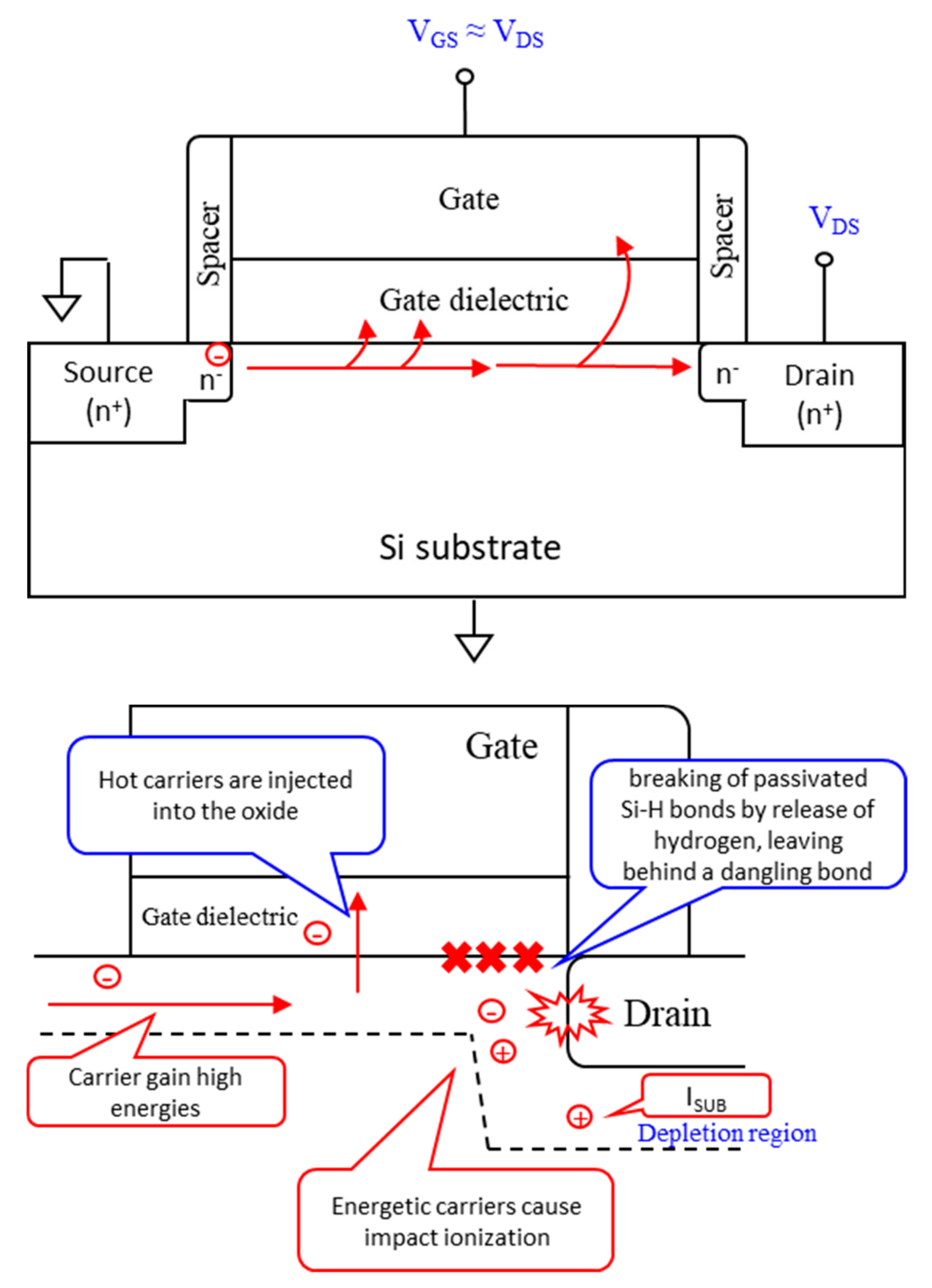
Figure 2.
Major mechanism of drain-avalanche-hot-carrier generation.

Figure 3.
Schematic cross-section profile of an n-channel metal–oxide–semiconductor field-effect transistor (n-MOSFET).
Figure 3.
Schematic cross-section profile of an n-channel metal–oxide–semiconductor field-effect transistor (n-MOSFET).

Figure 4.
(a) The impact ionization compared with different channel lengths; (b) substrate current with different channel lengths of n-MOSFETs.
Figure 4.
(a) The impact ionization compared with different channel lengths; (b) substrate current with different channel lengths of n-MOSFETs.

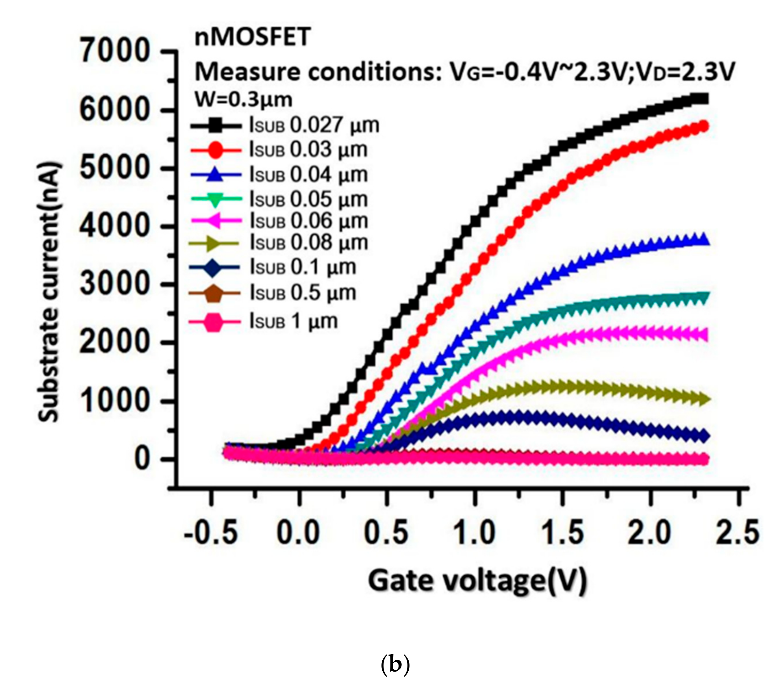
Figure 5.
In channel-hot-carrier (CHC) test conditions, the ISUB at: (a) W/L = 0.5/0.03 μm/μm, stressed at VGS = VDS = 1.2 V, (b) W/L= 0.5/0.03 μm/μm, stressed at VGS = VDS = 1.6 V, (c) W/L= 0.5/0.11 μm/μm, stressed at VGS = VDS = 1.2 V, and (d) W/L = 0.5/0.11 μm/μm, stressed at VGS = VDS = 1.6 V.
Figure 5.
In channel-hot-carrier (CHC) test conditions, the ISUB at: (a) W/L = 0.5/0.03 μm/μm, stressed at VGS = VDS = 1.2 V, (b) W/L= 0.5/0.03 μm/μm, stressed at VGS = VDS = 1.6 V, (c) W/L= 0.5/0.11 μm/μm, stressed at VGS = VDS = 1.2 V, and (d) W/L = 0.5/0.11 μm/μm, stressed at VGS = VDS = 1.6 V.

Figure 6.
In CHC test conditions, the VT shift at: (a) W/L = 0.5/0.03 μm/μm, stressed at VGS = VDS = 1.2 V, (b) W/L = 0.5/0.03 μm/μm, stressed at VGS = VDS = 1.6 V, (c) W/L = 0.5/0.11 μm/μm, stressed at VGS = VDS = 1.2 V, and (d) W/L = 0.5/0.11 μm/μm, stressed at VGS = VDS = 1.6 V.
Figure 6.
In CHC test conditions, the VT shift at: (a) W/L = 0.5/0.03 μm/μm, stressed at VGS = VDS = 1.2 V, (b) W/L = 0.5/0.03 μm/μm, stressed at VGS = VDS = 1.6 V, (c) W/L = 0.5/0.11 μm/μm, stressed at VGS = VDS = 1.2 V, and (d) W/L = 0.5/0.11 μm/μm, stressed at VGS = VDS = 1.6 V.

Figure 7.
In drain-avalanche-hot carrier (DAHC) test mode, the ISUB at: (a) W/L = 0.5/0.07 μm/μm, stressed at VGS at ISUB_max plus VDS = 1.4 V, (b) W/L = 0.5/0.07μm/μm, stressed at VGS at ISUB_max and VDS = 1.6 V, (c) W/L = 0.5/0.11 μm/μm, stressed at VGS at ISUB_max and VDS = 1.4 V, and (d) W/L = 0.5/0.11 μm/μm, stressed at VGS at ISUB_max and VDS = 1.6 V.
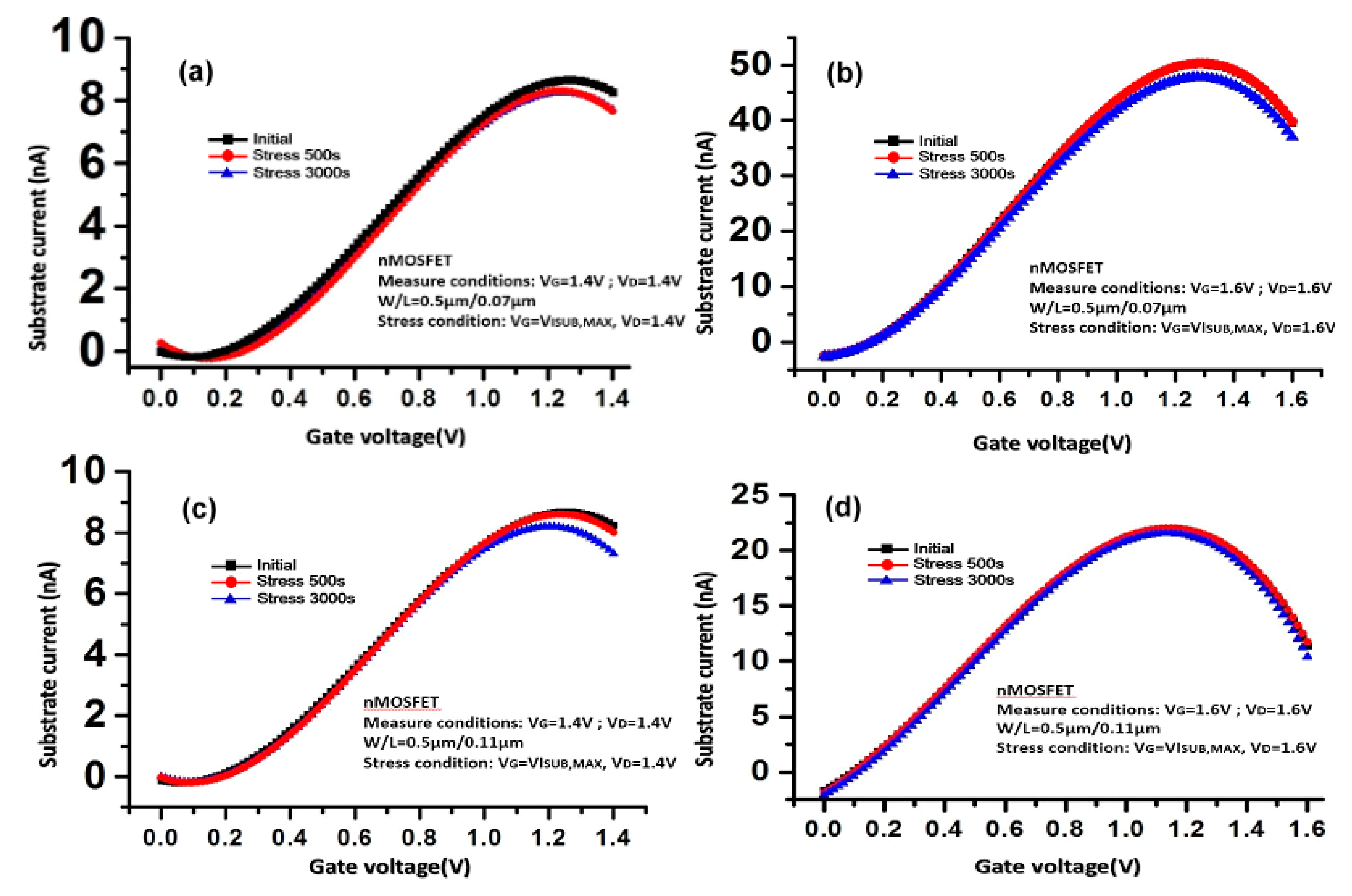
Figure 8.
In DAHC test mode, the VT shift at: (a) W/L = 0.5/0.07 μm/μm, stressed at VGS at ISUB_max plus VDS = 1.4 V, (b) W/L = 0.5/0.07 μm/μm, stressed at VGS at ISUB_max and VDS = 1.6 V, (c) W/L = 0.5/0.11 μm/μm, stressed at VGS at ISUB_MAX and VDS = 1.4 V, and (d) W/L = 0.5/0.11 μm/μm, stressed at VGS @ISUB_max and VDS = 1.6 V.

Figure 9.
n-MOSFETs lifetime data using the proposed model plotted on log (τ × IDS/W) versus ISUB/IDS.
Figure 9.
n-MOSFETs lifetime data using the proposed model plotted on log (τ × IDS/W) versus ISUB/IDS.

Figure 10.
(a) Simple band diagram of high-k (HK)-stacked HfOx/ZrOy/HfOz (HZH) structure operated at accumulation mode. EC: Conduction band, Ei: Intrinsic Fermi level, EF: Fermi level, and EV: Valence band, and (b) band offset for different dielectric compared with Si.
Figure 10.
(a) Simple band diagram of high-k (HK)-stacked HfOx/ZrOy/HfOz (HZH) structure operated at accumulation mode. EC: Conduction band, Ei: Intrinsic Fermi level, EF: Fermi level, and EV: Valence band, and (b) band offset for different dielectric compared with Si.

Figure 11.
The shift in interface trapped charge and oxide trapped charge after 3000 s CHC stress (W/L = 1/0.03 μm/μm) with decoupled plasma nitridation (DPN) or post-deposition annealing (PDA) treatments under 8% N2 concentration and annealing temperatures.
Figure 11.
The shift in interface trapped charge and oxide trapped charge after 3000 s CHC stress (W/L = 1/0.03 μm/μm) with decoupled plasma nitridation (DPN) or post-deposition annealing (PDA) treatments under 8% N2 concentration and annealing temperatures.

Figure 12.
The VT shift compared the CHC test with the DAHC test as the tested devices: (a) W/L = 0.5/0.07 μm/μm and (b) 0.5/0.11 μm/μm.
Figure 12.
The VT shift compared the CHC test with the DAHC test as the tested devices: (a) W/L = 0.5/0.07 μm/μm and (b) 0.5/0.11 μm/μm.


Table 1.
The comparison of quoted references [7,8,9,10,11,12,17,22] in the former and present process technologies.
| Reference | Purpose | Stress Method | Specifications |
|---|---|---|---|
| Takeda et al. [7] | Probing the DAHC injection and the substrate current-induced hot-electron injection (SCHE) under submicron process with gate dioxide. | DAHC and SCHE |
|
| Abramo et al. [8] | Using a Monte Carlo simulator to quantify the electron energy distribution in Si devices at low applied voltages involving the process of carrier heating. | DAHC |
|
| Yu et al. [9] | Exposing the hot-carrier effect related to the channel implantation process influencing the normal and reverse short-channel effect LDD MOSFETs down to 0.1 μm. | CHC |
|
| La Rosa et al. [10] | Reviewing the CHC mechanism and its effects on n-MOSFETs of deep submicron CMOS bulk technologies guided into the carrier dominant energy. | CHC |
|
| Mahapatra et al. [11] | Reviewing the physical mechanisms of transistor parameter shift due to hot-carrier degradation (HCD) in n-MOSFETs. | CHC and DAHC |
|
| Mahapatra et al. [12] | Reviewing the technology scaling including the stress temperature and performing the comparison of dc and ac stress | CHC under dc and ac stress |
|
| Acovic et al. [17] | Reviewing the hot-carrier effects and reliability problem in MOSFET | DAHC and ac stress |
|
| Amat et al. [22] | Presenting a comprehensive study on CHC degradation in short-channel MOSFETs with high-k dielectric | CHC and ac stress |
|
| This work | Studying the degradation mechanisms of substrate current for high-k MOSFETs after HC stresses and exposing the change mechanisms of values of the acceleration factor in lifetime calculation | CHC and DAHC |
|
Table 2.
Measurement conditions for ISUB values.
| Variable | Parameters Setup |
|---|---|
| Device width (µm) | 0.3 |
| Vcc (V) | 0.8 |
| Dimension (µm) | 0.027, 0.03, 0.04, 0.05, 0.06, 0.08, 0.1, 0.5, 1 |
| Stress conditions | VGS = −0.4 – 2.3 V; VDS = 2.3 V |
| Temperature (°C) | 25 |
Table 3.
Test conditions under HC stresses.
| Variable | Parameters Setup | |
|---|---|---|
| Device width (µm) | 0.5 | |
| Vcc (V) | 0.8 | |
| Stress mode | CHC | DAHC |
| Dimension (µm) | 0.03, 0.07, 0.11 | |
| Vstress | VGS = VDS = 1.2 V, 1.4 V, 1.6 V | VGS at ISUB, max; VDS = 1.2, 1.4, 1.6 V |
| Temperature (°C) | 25 | |
| Threshold Voltage (VT) | Constant current method to extract VT values, VT, lin = VGS at IDS = 300 nA × W/L, VDS = 0.1 V, VB = VS = 0 V | |
Publisher’s Note: MDPI stays neutral with regard to jurisdictional claims in published maps and institutional affiliations. |
© 2020 by the authors. Licensee MDPI, Basel, Switzerland. This article is an open access article distributed under the terms and conditions of the Creative Commons Attribution (CC BY) license (http://creativecommons.org/licenses/by/4.0/).
Share and Cite
MDPI and ACS Style
Chen, C.-W.; Wang, M.-C.; Chang, C.-H.-T.; Chu, W.-L.; Sung, S.-P.; Lan, W.-H. Hot Carrier Stress Sensing Bulk Current for 28 nm Stacked High-k nMOSFETs. Electronics 2020, 9, 2095. https://doi.org/10.3390/electronics9122095
AMA Style
Chen C-W, Wang M-C, Chang C-H-T, Chu W-L, Sung S-P, Lan W-H. Hot Carrier Stress Sensing Bulk Current for 28 nm Stacked High-k nMOSFETs. Electronics. 2020; 9(12):2095. https://doi.org/10.3390/electronics9122095
Chicago/Turabian StyleChen, Chii-Wen, Mu-Chun Wang, Cheng-Hsun-Tony Chang, Wei-Lun Chu, Shun-Ping Sung, and Wen-How Lan. 2020. "Hot Carrier Stress Sensing Bulk Current for 28 nm Stacked High-k nMOSFETs" Electronics 9, no. 12: 2095. https://doi.org/10.3390/electronics9122095
Note that from the first issue of 2016, this journal uses article numbers instead of page numbers. See further details here.