Article

Low Voltage Time-Based Matrix Multiplier-and-Accumulator for Neural Computing System

1
Electrical and Computer Engineering, The University of Texas at Austin, Austin, TX 78712, USA
2
Qualcomm Technologies Inc., San Diego, CA 92121, USA
3
Department of Electronics and Control Engineering, Hanbat National University, Daejeon 34158, Korea
4
School of Electronics Engineering, Kyungpook National University, Daegu 41566, Korea
5
School of Electronic and Electrical Engineering, Kyungpook National University, Daegu 41566, Korea
*
Author to whom correspondence should be addressed.
Electronics 2020, 9(12), 2138; https://doi.org/10.3390/electronics9122138
Submission received: 26 October 2020 / Revised: 8 December 2020 / Accepted: 11 December 2020 / Published: 14 December 2020
(This article belongs to the Special Issue Energy Efficient Circuit Design Techniques for Low Power Systems)

Abstract

:
A time-based matrix multiply-and-accumulate (MAC) operation for a neural computing system is described. A simple and compact time-based matrix MAC structure is proposed that can perform multiplication and accumulation simultaneously in a single multiplier structure, and the hardware complexity is not affected by the matrix input size. To enhance the linearity of the weight factor, an offset-free pulse-width modulator is introduced. The proposed MAC architecture operates at a low supply voltage of 0.5 V while it consumes MAC energy of 0.38 pJ with a 32 nm low-power (LP) predictive technology model (PTM) CMOS process. In addition, the near-subthreshold operation can remove the level shifter to interface between the MAC operator and digital circuits such as static random-access-memory (SRAM) because both can utilize the same level of the supply voltage. The proposed MAC is based on a digital intensive pulse-width modulation, and thus it can further improve its performance and area with more advanced technologies.

1. Introduction

Over several decades since 1950s, scientific communities strived to realize artificial intelligence based on the neural network and this classical topic recently gained the popularity with a gigantic surge of machine learning applications [1,2,3]. Relevant applications include computer vision [4,5,6,7,8,9,10,11,12], speech recognition [13,14], and medical applications [15,16,17,18], where the machine learning lies at the core of the technology and extracts meaningful data.
The matrix multiply-and-accumulate (MAC) is an essential operation for scientific computing, real-time signal processing, and machine learning. Several integrated circuit designs have demonstrated neural networks based on the MAC operation. An image recognition chip using neural networks has been demonstrated in [7]. To mimic neural networks, 256 neurons are used to compute the signal originating from synapses and 256 × 256 binary synapses to save the weight factors. A neuron comprises a digital type 16-bit adder and comparator. A static random-access-memory (SRAM) is used for 256 × 256 synapses. The operating frequency and supply voltage are 1 MHz and 0.55 V, respectively. The total chip size is 4.2 mm2 with 45-nm CMOS technology, and 2500 μm2 of the total area is occupied by 256 neurons. Compared with the work in [7], Merolla et al. proposed an enhanced image recognition chip using a larger number of neurons and synapses [8]. One million neurons and 256 million synapses were used. Consequently, the total area of the chip was 4.3 cm2 with 28-nm CMOS technology and the power consumption reached 72 mW at 0.775 V operating voltage. These representative works proved the benefits of neural network implementation on the integrated circuit but two major concerns on the area and power consumption arose due to the large number of neurons and synapses. To minimize these problems, a memristor was used [19]. Two characteristics of memristor, i.e., the small memristor size with respect to their functionality and ability to connect to the memristors using crossbars, can decrease the area and power overhead attributed to a large number of neurons and synapses. However, this approach has not been implemented to demonstrate neural networks.
Analog signal processing can be an alternative solution to alleviate the limitations of area and power consumption of digital implementations for neuromorphic computing. Using an analog MAC operator for a neuron instead of the digital approach can significantly improve the area and power consumption performances, since the number of transistors required for the analog adder and multiplier is substantially less. An analog MAC operator may exhibit the in-accuracy in its calculation, however it is not a problem because of the approximation characteristics of the neural network.
As an important application of neuromorphic computing, a self-calibrating GPS accelerator [20] requires four-dimensional data acquisition and processing (X, Y, Z, and time) for correlation calculation. The correlation calculation is performed by adding the multiplication result of the received signal with the time-shifted correlation pattern requiring large numbers of addition operations. Unlike conventional digital processing, correlating calculation can be performed in the analog domain using a current-mode summation with a current digital-to-analog converter (DAC). Thus, the addition of one more adder, instead of a larger adder tree, into the system enables the design to possess a single current control cell. In addition to the area and design complexity, the correlation result can exhibit a narrow dynamic range using a matched filter that allows a high resolution. Authors in [20] reported that the efficiency of the accelerator increased by 65 times while maintaining similar performance.
Multiplication is another significant burden on hardware, leading to a large area and processing time in digital VLSI circuits. A passive multiplication method using a capacitive DAC array is proposed [21,22]. This utilizes the advantages of charge conservation and redistribution which can be used in an energy-efficient computing system. Moreover, the offset problem in analog systems did not affect performance in the approximate computing applications. Similarly, a successive approximation (SAR) analog-to-digital converter (ADC), which comprises a conventional capacitor DAC array in series with another capacitor array to create a feedback divider, was used as a digitally controlled analog multiplier [9]. An electrocardiogram (ECG) based cardiac-arrhythmia detector and image-pixel-based gender detector were demonstrated using this system. A switched-capacitor MAC approach was reported in [10] such that the MAC operation was performed in three phases: (1) sampling and charge multiplication, (2) charge accumulation, and (3) SAR ADC digitization. The multiplying coefficients are determined by the capacitor ratio in the switched-capacitor network, and they can be adjusted based on the optimization results from the classifier-training kernel. An image classifier front end and an analog accelerator for classifier training were demonstrated.
Although power and area saving are the major advantages of the analog MAC approach, the analog implementation requires a higher supply voltage than digital circuits since the transistor in saturation requires higher voltage headroom and more transistor stacking is required in the analog circuit. Co-existence with the analog MAC and the other digital circuits needs to be considered as well. Because the digital circuit typically operates at the near-subthreshold region to save power [7,8], the analog MAC also desires to operate in the same supply voltage level used in the digital circuit.
In this work, a time-based matrix MAC operator for neural computing is proposed. In the conventional time-based MAC operation, a weighted multiplication is implemented by varying the time-delay or pulse-width, and the accumulation is achieved by adding multiple delay-based multiplier units [23,24]. Therefore, it requires as many multiplier units as the number of inputs to accumulate each time-delay. In the proposed design, the input data is converted into the analog signal by input current DAC, and a time-based multiplication is implemented by the pulse-width modulator and the sample-and-hold circuit. The accumulation is performed simultaneously in the multiplication circuit such that the proposed MAC does not require multiple multiplier units.
The proposed design can easily increase the number of inputs without the burden of hardware complexity. Due to the time-based operation, it can operate in the near-threshold region for energy saving. Moreover, the near-subthreshold operation can remove the level shifter to interface between the matrix multiplier and the digital circuits, because both can utilize the same supply voltage.
This paper is organized as follows. Section 2 introduces the principle of the time-based MAC operation. Section 3 describes the circuit implementation of the matrix MAC operator. Section 4 provides the simulated results and the conclusion remarks are given in Section 5.

2. Time-Based Analog Multiplier

2.1. Conventional Analog Implementation

Generally, the characteristics of charge conservation and Kirchhoff’s current law (KCL) are used to implement the analog MAC operation as shown in Figure 1. Based on the charge conservation, VOUT in Figure 1a can be written as
V O U T   =   C 1 C 1   +   C 2 V I N
Equation (1) has a multiplication form, and the multiplier can be easily adjusted by changing the ratio of the capacitances. However, this approach has a disadvantage in terms of area because many capacitor arrays are required for the matrix multiplier. To reduce area overhead, establishing a small unit capacitance is desired. For example, a fringe capacitor of 300 aF was used in [10], albeit this small capacitance makes the circuit sensitive to a process mismatch.
Figure 1b shows the analog summation using KCL. IOUT is the summation of the currents flowing into the node (VX). Then, it can be expressed as
I O U T   =   I 1 + I 2 + + I n
This approach has a significant disadvantage in the aspect of power consumption because many current sources are needed.
An operational transconductance amplifier (OTA) was used to incorporate both multiplication and summation in the voltage domain, as shown in Figure 1c. The output can be expressed as
V O U T   =   C 1 C S V 1 + C 2 C S V 2 + +   C n C S V N
However, this implementation suffers from the problem of excessive noise arising from the OTA. Moreover, the bandwidth of the OTA should be wider than the input rate, which is difficult to design with the limited supply voltage and power consumption.

2.2. Proposed Time-Based Implementation

To resolve the problems of the conventional voltage-domain analog implementation, a time-based operation can be utilized. In the conventional time-based MAC structure, the weighted multiplication is implemented by the variable time-delay unit and the accumulation is done by sequentially adding the multiplier units [23,24]. Therefore, it requires as many multiplier units as the number of inputs such that it may cause high complexity for a large matrix input.
A simple and compact time-based MAC operator is proposed which can perform the multiplication and accumulation simultaneously. Figure 2 shows the proposed time-based multiplier that consists of a sample-and-hold circuit with a current input signal (IIN). A switch in the sample-and-hold circuit is controlled by the pulse-width-modulated (PWM) signal. Hence, the output voltage can be expressed as
V O U T   =   t p w C S I I N
where, tpw is the time of PWM signal and CS is the sampling capacitor in the sample-and-hold circuit. The output voltage is shown as a multiplication form and the coefficient of the multiplier can be easily adjusted by varying the pulse-width.
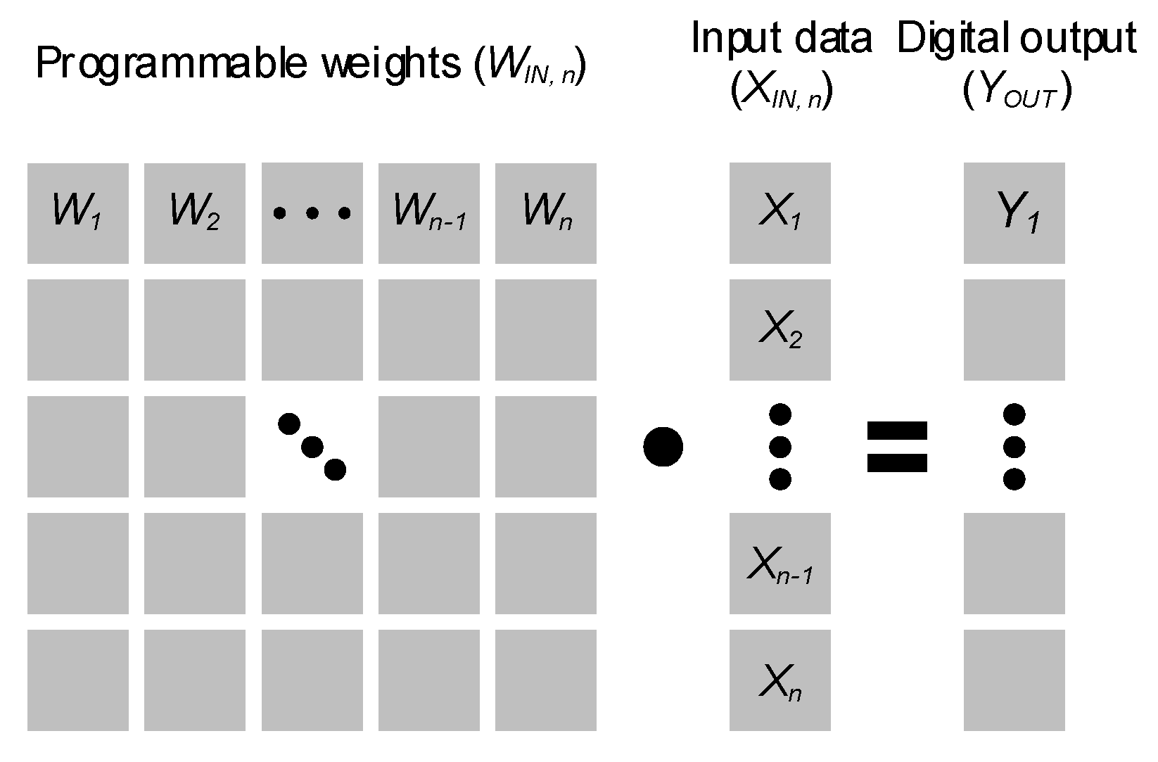
Figure 3 shows the vector-by-matrix multiplication. The input data (XIN) such as images or any user-generated signals are multiplied with a programmable weighted matrix (WIN) and generate accumulated digital output (YOUT). Applying the input data information and weighted factor by varying the IIN and tpw, respectively, at every sampling cycle, both the multiplication and accumulation are obtained simultaneously in the proposed time-based multiplier (Figure 2). The output of the sample-and-hold circuit including the MAC operation can be expressed as
V O U T   =   t p w , 1 C S I I N , 1 + t p w , 2 C S I I N , 2 + +   t p w , n C S I I N , n
Although conventional time-based MAC operators require multiple time-based multiplier units in proportion to the input matrix size, the proposed time-based MAC operation is achieved only by a single-multiplier unit, regardless of the input matrix size.
The time-based multiplier has significant benefits in terms of area and power consumption. The pulse-width control circuit can be implemented by digital logic, hence, a large capacitor array is not required. Moreover, the lower supply voltage limitation due to an OTA does not exist in the proposed structure. Furthermore, digital gates can be easily operated in the near-threshold region, implying high power efficiency.

3. Circuit Implementation

The time-based matrix MAC operator comprises the input current DAC, a sample-and-hold, SAR ADC, and a pulse-width modulator as shown in Figure 4a. The input data is converted into the analog signal by the input current DAC and then time-based multiplication is performed by the pulse-width modulator and the sample-and-hold circuit. The accumulation is performed by adding the charge of each multiplication cycle into the same sampling capacitor, CS. Figure 4b shows the timing diagram of the proposed time-based MAC operation. A complete computation involves 64 cycles (n = 64), indicating that the number of required current DACs and ADCs is decreased by 64×. The ADC operation is simultaneously executed for previous accumulated output data to increase the operating frequency of the matrix multiplier. After the computation, the ADC samples the output again and then the sampling capacitor is initiated for the next computation.

3.1. Proposed Offset-Free Pulse-Width Modulator

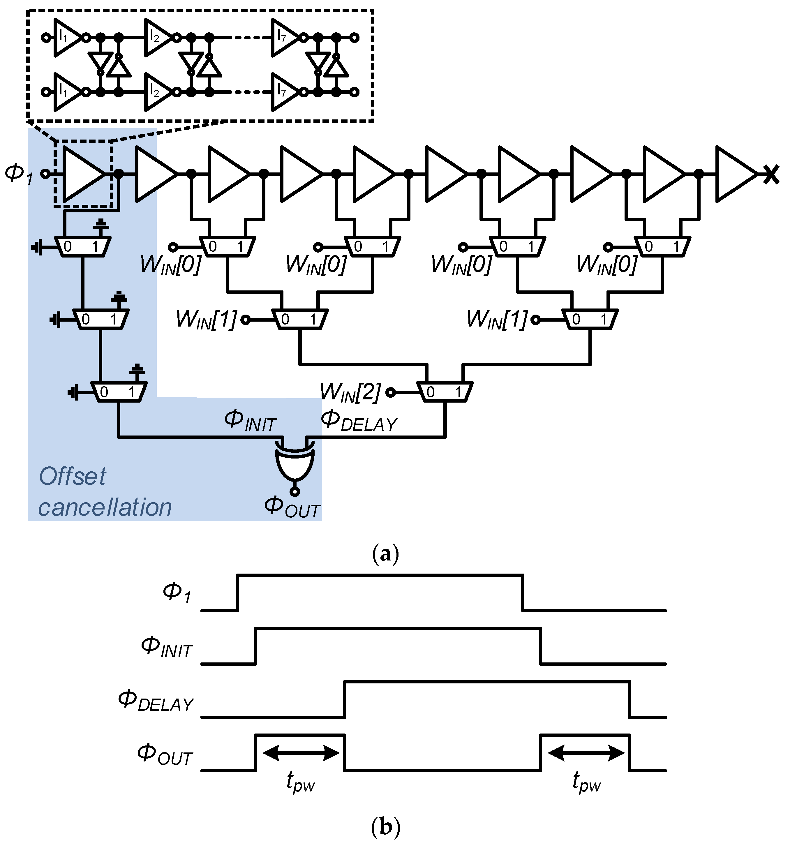
The pulse-width modulator has a 3-bit weighted input such that it can generate 8 different pulse-widths. Figure 5 shows the proposed offset-free digital intensive pulse-width modulator and its timing diagram. To generate different pulse-widths, the delay line comprising 10 delay units is used. Each delay unit comprises 7 cross-coupled inverters for differential pulse output. To isolate the pulse-width variation from the effect of input slope and loading capacitance, two additional buffers are added to the first and last stage of the delay line. Achieving a good linearity of the delay without offset delay is crucial. If the offset delay is added to the multiplier, the result of the multiplier can be inaccurate. The offset delay is caused by the additional multiplexer which selects the delay line from the weighted control code (WIN). To remove the offset delay, the first stage output also uses the dummy multiplexers to match the propagation delay. After that, the first stage output and the delayed signal output are both fed into the XOR gate to generate two pulses for every one input signal. Hence, (4) can be modified as follows
V O U T   =   2 × t p w C S I I N
The supply voltage of 0.5 V is used for the near-threshold operation. Consequently, the delay resolution of the delay line is 15 ns and its delay variation shows a very linear characteristic with the control code, as shown in Figure 6.

3.2. SAR ADC

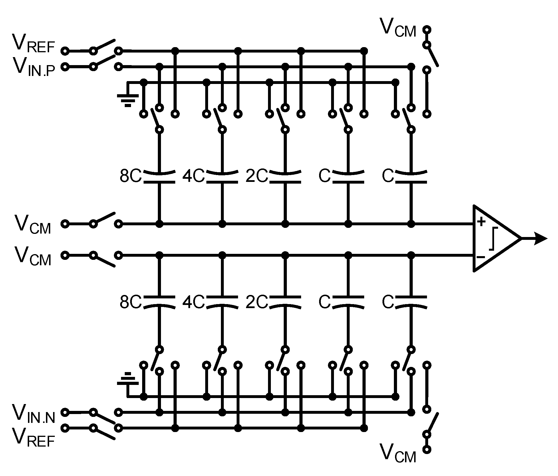
A fully differential SAR ADC is designed to convert the analog voltage back to the digital domain. A SAR ADC has an advantage of a small area such that it is good for applications requiring a large number of ADCs in an array. A 6-bit ADC is designed in this application, as shown in Figure 7. To reduce the number of capacitors in the capacitive DAC array with the unit cap of 4 fF, the bidirectional single-sided switching algorithm is used in the design. A 98% power saving can be achieved and the size of the MSB capacitor can be reduced by 4 times. Thus, the area of the capacitor requiring most of the area in the system is saved by 75% compared with the conventional switching scheme.
The charge in the storing capacitor is redistributed with the capacitor array of the SAR ADC, which can limit the swing of data. However, in this design, the error and limitation of the swing is less than 0.16% because the total capacitance of the array is 16 fF, which is negligible compared with that of the storage capacitor.
The ADC performs a 6-bit resolution with power less than 2.38 nW at 27.8 kS/s with a 0.5 V supply voltage. SNDR shows 34.7 dB that corresponds to an ENOB of 5.5 bits. Since the tested input is not full swing, a 3-dB drop is expected in the SNDR.

3.3. Input Current DAC

Although it is difficult to operate the MOSFET in the saturation region with a 0.5 V power supply, a current mirror can be implemented in the subthreshold region [25,26]. The MOSFET drain current in the subthreshold region can be expressed as
i D   =   ( n 1 ) μ C o x W L V T 2 e V G S V T H n V T ( 1 e V D S V T )
where n is the subthreshold ideality factor, μ is the mobility, COX is the oxide capacitance per unit area, VTH is the threshold of the transistor and VT = kT/q is the thermal voltage, which is 26 mV at room temperature. If VDS is significantly larger than VT, Equation (7) can be approximately written as follows:
i D ( n 1 ) μ C o x W L V T 2 e V G S V T H n V T   =   I S 0 W L e V G S V T H n V T
Applying IREF and iu for the case of the PMOS current mirror (Figure 8a) into Equation (8), IREF and iu can be expressed as
I R E F   =   I S 0 W P 1 L P 1 e V B I A S . P V T H n V T
i u   =   I S 0 W P 2 L P 2 e V B I A S . P V T H n V T
Hence, the relationship between the two currents IREF and iu can be expressed as
i u   =   L P 1 L P 2 W P 2 W P 1 I R E F
Equation (11) shows that the current can be mirrored using the ratio of widths and lengths. Based on these equations, the current unit for a source and sink is configured as shown in Figure 8a,b, respectively.
The input current DAC is fully differential and subsequently drives the SAR ADC. Figure 8c shows the single-ended half-circuit for illustration. The input current of the DAC comprises the current mirrors for the current source and sink and resistors for the reset operation. The input of the current DAC is 6 bits with the MSB as a sign-bit. In our design, the 1’s complement signed number is adopted due to its simplicity while sacrificing only 3% for negative number representation. To achieve a good matching property, each current mirror consists of the same current unit size with a different number of units. Moreover, a long channel is used for the current mirror to increase the output impedance, minimize the leakage current, and mitigate the mismatch from the process variation. The unit transistor size for the current source/sink unit (Figure 8a,b) is set to W = 2 μm and L = 4 μm. Consequently, sufficient linearity of the 6-bit input current DAC is achieved, as shown in Figure 9.

4. Simulation Results

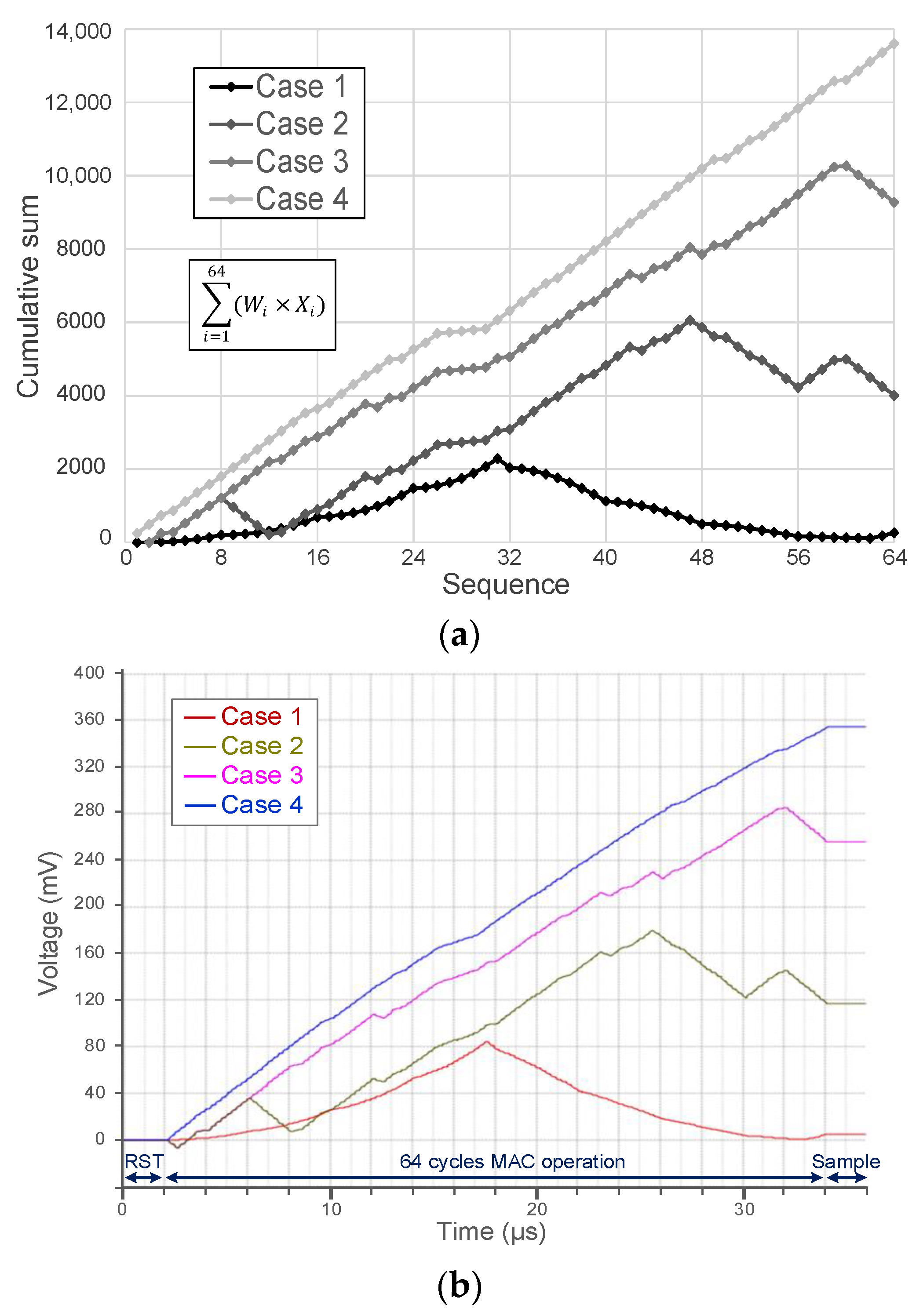
The proposed time-based matrix multiplier is implemented using a 32 nm low-power (LP) predictive technology model (PTM) CMOS process with a 0.5 V supply voltage. An important fact for the matrix MAC with an ADC is that the output is not the true value, but a scaled value. This is because the transitions from the digital input to the analog input and from the analog output to the digital output during the computation involve a scaling process. In particular, the analog output must be converted by an ADC and thus the output of the operator is scaled by the number of output bits of the ADC. To extract the exact scaling factor, the output values of the ADC are measured for minimum and maximum inputs. After translating the ADC output from the [0:63] range to the [−32:31] range, since the input has both a negative and a positive range, the ADC output shows −24 when the input is minimum while it shows 23 when the input is maximum. The full range of the expected output is 31,744 because the minimum and maximum expected outputs are −15,872 (−31 × 8 × 64 cycles) and 15,872 (31 × 8 × 64 cycles), respectively. Hence, the scaling factor is 675 (=31,744/47).
To verify the MAC operation, the expected output value for the applied input values and output of the proposed matrix MAC are compared, as shown in Figure 10. Figure 10a shows the accumulated multiplier value during 64 cycles for four different cases, and Figure 10b shows the simulated differential output, which is the input voltage of the ADC. The actual time domain for the case from 1 to 4 is shifted to the same time domain for a clear view. Both the expected MAC output and simulated output show similar shape and the error of the ADC output is summarized in Table 1. Table 1 shows the computation results of the analog matrix multiplier with the various input vectors for all cases, as depicted in Figure 10a. For example, the expected final output of case 1 is 262. Considering the scaling factor of 675 and the limitation of the expression of the fractional part of the number in binary numbers, the final output of the analog matrix multiplier should be 0 (262/675 = 0.39). The simulated result shows that the ADC output after 64 cycles is 0 (6′b100000 − 2′d32), which matches well with the expected output. Most of calculation error is caused by the mismatch of the current mirror due to the channel length modulation by the different drain voltage, vDS, and the quantization error of the ADC. The result shows that the calculation error is around 1.
The proposed architecture consumes 1.5 μW and shows MAC energy (EMAC) of 0.38 pJ at a 2 MHz MAC rate in the simulation. The energy efficiency includes ADC, MAC, and DAC operation. Table 2 compares the architecture with prior works. It is difficult to lower the supply voltage for conventional analog-based structures due to the voltage headroom of analog circuits. Furthermore, the work in [10] used a switched-capacitor that required many analog switches. The size of the switches significantly increases with near-subthreshold operation under low supply voltage, which decreases the accuracy of the calculation and increases dynamic power consumption. Although the conventional time-based structures can avoid the headroom of the supply voltage, it requires many time-based multiplier units in proportion to the input matrix size [23,24]. The proposed structure can implement the MAC operation with a single multiplier regardless of the input matrix size.

5. Conclusions

The analog matrix MAC resolves the limits of chip area and power consumption from the digital arithmetic implementation although low supply voltage in the scaled CMOS process does not favor the conventional analog matrix MAC. In this work, we proposed the simple and compact time-based matrix MAC operator that can perform multiplication and accumulation simultaneously in a single multiplier structure. The proposed architecture avoids hardware complexity, even from the large matrix input, and also can operate at a 0.5 V supply voltage with an EMAC of 0.38 pJ. The near-subthreshold operation can avoid an interfacing circuit such as a level shifter when the analog and digital circuits utilize different supply levels. The pulse-width modulation for the proposed analog matrix MAC can further benefit in its performance and chip area through the use of more advanced technologies.

Author Contributions

Conceptualization, circuit modeling, and simulations, S.H., H.K.; analysis, S.H., H.K., J.K., K.C.; resources, J.K., K.C.; writing—original draft preparation, S.H., H.K., K.C.; writing—review and editing, J.K., K.C.; visualization, K.C.; supervision, J.K., K.C. All authors have read and agreed to the published version of the manuscript.

Funding

This work was supported by the National Research Foundation of Korea (NRF), from a grant funded by the Korean government (MSIT) (No. 2020R1G1A1100085).

Acknowledgments

The EDA tool was supported by the IC Design Education Center (IDEC), Korea.

Conflicts of Interest

The authors declare no conflict of interest.

References

  1. Sze, V.; Chen, Y.-H.; Emer, J.; Suleiman, A.; Zhang, Z. Hardware for machine learning: Challenges and opportunities. In Proceedings of the IEEE Custom Integrated Circuits Conference (CICC), Austin, TX, USA, 30 April–3 May 2017; pp. 1–8. [Google Scholar]
  2. Vanhoucke, V.; Senior, A.; Mao, M.Z. Improving the speed of neural networks on CPUs. In Proceedings of the Deep Learning and Unsupervised Feature Learning Workshop, NIPS, Granada, Spain, 16 December 2011. [Google Scholar]
  3. Lu, J.; Young, S.; Arel, I.; Holleman, J. A 1 TOPS/W Analog Deep Machine-Learning Engine With Floating-Gate Storage in 0.13 µm CMOS. IEEE J. Solid-State Circuits 2015, 50, 270–281. [Google Scholar] [CrossRef]
  4. Cisco Visual Networking Index (VNI) Complete Forecast Update. Available online: https://www.cisco.com (accessed on 1 January 2016).
  5. Woodhouse, J. Big, Big, Big Data: Higher and Higher Resolution Video Surveillance. Available online: http://technology.ihs.com (accessed on 1 January 2016).
  6. Szeliski, R. Computer Vision: Algorithms and Applications; Springer: London, UK, 2010. [Google Scholar]
  7. Seo, J.-S.; Brezzo, B.; Liu, Y.; Parker, B.D.; Esser, S.K.; Montoye, R.K.; Rajendran, B.; Tierno, J.A.; Chang, L.; Modha, D.S.; et al. A 45nm CMOS neuromorphic chip with a scalable architecture for learning in networks of spiking neurons. In Proceedings of the IEEE Custom Integrated Circuits Conference (CICC), San Jose, CA, USA, 18–21 September 2011; pp. 1–4. [Google Scholar]
  8. Merolla, P.A.; Arthur, J.V.; Alvarez-Icaza, R.; Cassidy, A.S.; Sawada, J.; Akopyan, F.; Jackson, B.L.; Imam, N.; Guo, C.; Nakamura, Y.; et al. A million spiking-neuron integrated circuit with a scalable communication network and interface. Science 2014, 345, 668–673. [Google Scholar] [CrossRef] [PubMed]
  9. Zhang, J.; Wang, Z.; Verma, N. A matrix-multiplying ADC implementing a machine-learning classifier directly with data conversion. In Proceedings of the IEEE International Solid-State Circuits Conference (ISSCC) Digest of Technical Papers, San Francisco, CA, USA, 22–26 February 2015; pp. 332–333. [Google Scholar]
  10. Lee, E.H.; Wong, S.S. Analysis and Design of a Passive Switched-Capacitor Matrix Multiplier for Approximate Computing. IEEE J. Solid-State Circuits 2016, 52, 261–271. [Google Scholar] [CrossRef]
  11. Rieutort-Louis, W.; Moy, T.; Wang, Z.; Wagner, S.; Sturm, J.C.; Verma, N. A Large-Area Image Sensing and Detection System Based on Embedded Thin-Film Classifiers. IEEE J. Solid-State Circuits 2015, 51, 281–290. [Google Scholar] [CrossRef]
  12. Wang, Z.; Zhang, J.; Verma, N. Realizing Low-Energy Classification Systems by Implementing Matrix Multiplication Directly Within an ADC. IEEE Trans. Biomed. Circuits Syst. 2015, 9, 1. [Google Scholar] [CrossRef] [PubMed]
  13. Price, M.; Glass, J.; Chandrakasan, A.P. A 6 mW, 5,000-Word Real-Time Speech Recognizer Using WFST Models. IEEE J. Solid-State Circuits 2014, 50, 102–112. [Google Scholar] [CrossRef]
  14. Yazdani, R.; Segura, A.; Arnau, J.-M.; Gonzalez, A. An ultra low-power hardware accelerator for automatic speech recognition. In Proceedings of the IEEE/ACM International Symposium on Microarchitecture (MICRO), Taipei, Taiwan, 15–19 October 2016; pp. 1–12. [Google Scholar]
  15. Verma, N.; Shoeb, A.; Guttag, J.V.; Chandrakasan, A.P. A micro-power EEG acquisition SoC with integrated seizure detection processor for continuous patient monitoring. In Proceedings of the IEEE Symposium on VLSI Circuits, Kyoto, Japan, 16–18 June 2009; pp. 62–63. [Google Scholar]
  16. Chen, T.-C.; Lee, T.-H.; Chen, Y.-H.; Ma, T.-C.; Chuang, T.-D.; Chou, C.-J.; Yang, C.-H.; Lin, T.-H.; Chen, L.-G. 1.4µW/channel 16-channel EEG/ECoG processor for smart brain sensor SoC. In Proceedings of the IEEE Symposium on VLSI Circuits, Honolulu, HI, USA, 16–18 June 2010; pp. 21–22. [Google Scholar]
  17. Lee, K.H.; Verma, N. A Low-Power Processor with Configurable Embedded Machine-Learning Accelerators for High-Order and Adaptive Analysis of Medical-Sensor Signals. IEEE J. Solid-State Circuits 2013, 48, 1625–1637. [Google Scholar] [CrossRef]
  18. Bin, A.M.; Yoo, J. A 1.83 μJ/classification, 8-channel, patient-specific epileptic seizure classification SoC using a non-linear support vector machine. IEEE Trans. Biomed. Circuits Syst. 2016, 10, 49–60. [Google Scholar]
  19. Ebong, I.E.; Mazumder, P. CMOS and Memristor-Based Neural Network Design for Position Detection. Proc. IEEE 2011, 100, 2050–2060. [Google Scholar] [CrossRef]
  20. Skrzyniarz, S.; Fick, L.; Shah, J.; Kim, Y.; Sylvester, D.; Blaauw, D.; Fick, D.; Henry, M.B. A 36.8 2b-TOPS/W self-calibrating GPS accelerator implemented using analog calculation in 65nm LP CMOS. In Proceedings of the IEEE International Solid-State Circuits Conference (ISSCC), San Francisco, CA, USA, 31 January–4 February 2016; pp. 420–422. [Google Scholar]
  21. Bankman, D.; Murmann, B. Passive charge redistribution digital-to-analogue multiplier. Electron. Lett. 2015, 51, 386–388. [Google Scholar] [CrossRef]
  22. Joshi, S.; Kim, C.; Ha, S.; Chi, Y.M.; Cauwenberghs, G. 2pJ/MAC 14b 8×8 linear transform mixed-signal spatial filter in 65nm CMOS with 84dB interference suppression. In Proceedings of the IEEE International Solid-State Circuits Conference (ISSCC), San Francisco, CA, USA, 5–9 February 2017; pp. 364–365. [Google Scholar]
  23. Miyashita, D.; Kousai, S.; Suzuki, T.; Deguchi, J. A Neuromorphic Chip Optimized for Deep Learning and CMOS Technology With Time-Domain Analog and Digital Mixed-Signal Processing. IEEE J. Solid-State Circuits 2017, 52, 2679–2689. [Google Scholar] [CrossRef]
  24. Everson, L.; Liu, M.; Pande, N.; Kim, C.H. An Energy-Efficient One-Shot Time-Based Neural Network Accelerator Employing Dynamic Threshold Error Correction in 65 nm. IEEE J. Solid-State Circuits 2019, 54, 2777–2785. [Google Scholar] [CrossRef]
  25. Gilbert, B. Translinear circuits: An historical overview. Analog. Integr. Circuits Signal Process. 1996, 9, 95–118. [Google Scholar] [CrossRef]
  26. Vittoz, E.; Fellrath, J. CMOS analog integrated circuits based on weak inversion operations. IEEE J. Solid-State Circuits 1977, 12, 224–231. [Google Scholar] [CrossRef] [Green Version]
Figure 1. Conventional analog operators: (a) analog multiplication using charge conservation, (b) analog summation using Kirchhoff’s current law (KCL) and (c) analog multiplication and summation using an operational transconductance amplifier (OTA).
Electronics 09 02138 g001
Figure 2. Proposed time-based analog multiplier.
Electronics 09 02138 g002
Figure 3. Vector-by-matrix multiplication.
Electronics 09 02138 g003
Figure 4. Proposed time-based matrix multiply-and-accumulate (MAC): (a) system architecture and (b) timing diagram.
Electronics 09 02138 g004
Figure 5. Proposed offset-free digital-intensive pulse-width modulator: (a) circuit diagram and (b) timing diagram.
Electronics 09 02138 g005
Figure 6. Simulated result of the pulse-width modulator for different weight code (WIN).
Electronics 09 02138 g006
Figure 7. Successive approximation (SAR) analog-to-digital converter (ADC) architecture.
Electronics 09 02138 g007
Figure 8. Input current DAC: (a) current source unit, (b) current sink unit, (c) half-circuit of the differential DAC.
Electronics 09 02138 g008
Figure 9. Simulated results of the input current digital-to-analog converter (DAC).
Electronics 09 02138 g009
Figure 10. Simulated results of the analog matrix multiplier: (a) expected accumulated multiplier value for different input vector cases and (b) simulated differential output plotted in the same time scale.
Electronics 09 02138 g010
Table 1. Output error for different input vectors.
Expected Scaled OutputADC OutputError
Case 10.390+0.39
Case 25.947−1.06
Case 313.7415−1.26
Case 420.1621−0.84
Table 2. Architecture comparison.
ProcessDomainSupply VoltageWeighted MultiplierAccumulator
[10]40 nmAnalog1.1 VSwitched-capacitor multiplier with variable capacitor ratioCharge accumulation
[9]130 nmAnalog1.2 VMultiplying ADC with variable capacitor ratioDigital adder by S/W
[22]65 nmAnalog1.2 VMultiplying DAC with variable capacitor ratioDigitally controlled VGA
[23]65 nmTime1 VVariable delay cellSequentially added
multiplier units
[24]65 nmTime0.7–1.4 VVariable delay cell with calibrationSequentially added
multiplier units
This work32 nmTime0.5 VVariable delay cell with offset-free structureCharge accumulation
Publisher’s Note: MDPI stays neutral with regard to jurisdictional claims in published maps and institutional affiliations.