A Novel General Purpose Combined DFVF/VCII Based Biomedical Amplifier


Department of Industrial and Information Engineering and Economics, University of L’Aquila, 67100 L’Aquila, Italy
*
Author to whom correspondence should be addressed.
Electronics 2020, 9(2), 331; https://doi.org/10.3390/electronics9020331
Submission received: 2 January 2020
/
Revised: 7 February 2020
/
Accepted: 11 February 2020
/
Published: 14 February 2020
(This article belongs to the Special Issue Low-Voltage Integrated Circuits Design and Application)
Abstract
:We here present a 0.15 µm CMOS high input impedance and low noise AC coupled flipped voltage follower-based amplifier for high integration level in integrated circuits in a wide range of sensing applications. With such a circuit, it is possible to achieve a high level of integration, thanks to the absence of passive resistors, and also to implement a very high input impedance without capacitive feedback thanks to bootstrap operation, thus offering a very low high-pass cutoff frequency. Simulated results with a proven and well modeled standard technology show a whole circuit input-referred noise of 5.4 µVrms. The bias voltage is ±0.6 V with a total power consumption of the single amplifier of 20 µW. The very low circuit complexity allows a very low estimated reduced area occupation giving, as a general example, the possibility of integrating an array of up to thousands of channels for biomedical applications. Detailed simulation results, PVT analysis and comparison tables are also presented in the paper.
1. Introduction
The acquisition and recording of low-frequency and low-amplitude signals for photonics, automotive, biomedical and structural applications is of fundamental importance in current electronic systems: as an example, the acquisition of very noisy signals is at the foundation of understanding brain functions [1,2,3,4,5,6,7,8,9,10]. Bioelectric signal sensing, in particular, is a challenging feature in both daily healthcare and prevention.
A general electrical biosignal is characterized by very low amplitude and also by the fact that is buried in noise. As widely reported in the literature, neuro signals have a very low electrical amplitude, up to 1 mVpp, and their frequency ranges between 0.5 Hz and 10 kHz. They can be classified into two groups: local-field potentials (LFPs) and action potentials (APs). The first group is characterized by very slow signals, where the frequency is in the range ∼ (0.5 Hz–1 kHz), while in the second group, the neuro signals present a rapid amplitude variation forming a series of spikes; therefore, the frequency is higher and falls in the range ∼ (0.3 Hz–10 kHz). Moreover, these signals are characterized by an amplitude that is inversely proportional to the frequency, causing faster signals, such as AP to have an even smaller amplitude; therefore, proper amplification is required. With respect to heart signal monitoring, all the information for electrocardiography (ECG) is located in the ∼ (0.05 Hz–100 Hz) range, while the voltage amplitude, considering conventional wet cloth electrodes, is below 0.5 V [11]. A challenging aspect of designing a general-purpose amplifier, however, is that there are applications where, instead, a large bandwidth may be of importance, as presented in [12,13]. A compromise is therefore necessary for the overall performance of the circuit.
In the literature, many electronic circuits and systems have been proposed in order to interface with and sense very low voltage signals from dedicated or general-purpose electrodes [14,15,16,17,18,19,20], even for portable application [21], where the energy consumption is much more critical and energy harvesting techniques can be employed to remove the battery dependence or at least to increase the lifetime [22,23,24,25,26]. As a rule, the performances of these interfacing circuits, including, in most cases, buffers or amplifiers as a first stage, are limited by the DC gain, DC offset, noise, Common Mode Rejection Ratio (CMRR), and input impedance. Also, dimensions and power consumption are important features, especially in very low voltage, very low power applications, and also the limiting of heat dissipation. Finally, the on-chip area occupation, in addition to the features listed above, is often a fundamental requirement. Due to all the aforementioned aspects, electronic recording circuits and systems require a very low noise first interfacing stage that in most cases is formed by a high-impedance input voltage amplifier. Several architectures implementing such circuits have been proposed in the literature [27,28,29,30,31,32,33], but there is a continuous demand for novel and improved-performance topologies in order to achieve an ultra-large-scale integrated solution. In particular, in the biomedical acquisition system literature, different electronic interfaces have been proposed, in order to minimize the interference voltage contribution, usually by achieving a very high input impedance and high CMRR values. Most of these solutions are centered on the analysis of the frontend amplifier, which has to perform a differential reading with appropriate noise rejection; hence, its performance affects the overall behavior of the whole system.
In this work, in order to overcome the mentioned specifications tradeoff in terms of noise, power consumption, gain and space occupancy we propose a low complexity mixed operation mode (voltage/current) amplifier using two different circuit architectures. In particular, we combine a Differential Flipped Voltage Follower (DFVF) stage with a Second-Generation Voltage Conveyor (VCII) acting as transimpedance amplifier.
The proposed circuit was simulated in LTspice using a standard CMOS technology with very accurate 0.15 um foundry models, comparing the performance with state-of-the-art circuits. The proposed circuit has an input-referred noise of 5.4 µVrms. The supply voltage is ±0.6 V, with a total power consumption of the single amplifier of 20 µW.
This paper is organized as follows. In Section 2, a brief recall of DFVF and VCII are given while in Section 3 we describe in detail the proposed architecture and the design constraint of the proposed integrable circuit blocks. Simulation results are outlined in Section 4. Finally, Section 5 reports the conclusions of the paper.
2. Flipped Voltage Follower and Second-Generation Voltage Conveyor Short Overview
2.1. The Flipped Voltage Follower
The Flipped Voltage Follower (FVF) is basically a high input impedance low complexity high precision buffer. The FVF is also characterized by very low output impedance, requiring a very low static power dissipation.
The basic FVF circuit is reported in Figure 1a [34,35,36,37,38,39,40,41]. The applied signal Vin is buffered to the source of transistor Ml. In this case, a high value of input impedance, especially at low frequency, is given by the gate of transistor Ml, while a low output impedance is achieved due to the negative feedback loop implemented by the transistor M2. Concerning the bias condition, the current flowing through M1 is constant and fixed by the current generator IB. The circuit load current is given by varying the current through M2. Two different phases can be distinguished during normal operating conditions. The first phase is for the applied rising edge of Vin. In this case, the current is injected to the load; the transistor M1 current is fixed to IB while the M2 current in is reduced, with the load current now being equal to IL = IB−ID(M2). A maximum load current equal to IB is delivered to the load when M2 is switched off. In the second phase, the input signal falling edge is considered. In this case the current is taken from the load but, the current through M1 being constant, this means that the M2 current increases, and this is possible thanks to the negative feedback loop that increases the A node voltage increasing the gate applied voltage of M2. In this last case, the total current of M2 is given by IL + IB not being limited by IB, but rather only being limited by the supply voltage. The output impedance is always low for both phases while the input impedance remains the same (gate terminal impedance).
The presented conventional FVF has a major drawback: it can deliver a sink load current greater than the bias current, but is limited in terms of delivering a maximum load current of IB. For this reason, distortion phenomena may occur in normal operation when large input signals are applied, or extremely low operation voltages required. To overcome this limitation, improved topologies have been presented in the literature. For example, Figure 1b shows a modified FVF architecture that is able to deliver a load current larger than the applied bias. In this topology, the M1 current is not fixed by a constant current source as in Figure 1a; in this way, it can provide a load current in both phases that is greater than its bias current. The only limitation of this modified architecture is that during the second phase, when high input signals are applied, the feedback loop does not work properly anymore, and the buffer functionality is performed by the simple common drain transistor M1. In this last case, the FVF output impedance becomes 1/gm1, which is different from the first phase output impedance because the feedback is very low.
2.2. The Second-Generation Voltage Conveyor
Recently, current-mode signal processing and, in particular, the basic building block, namely the second-generation current conveyor (CCII), have been used instead of the Op-Amp in many integrated applications [42,43,44]. With respect to the classical Op-Amp, the CCII device is simpler and superior due to both the low complexity of the transistor level structure and, more importantly, its open-loop configuration. In fact, thanks to the absence of negative feedback, the frequency compensation is not needed, resulting in a further simplified circuit design and also high-frequency operation with the same performance as the Op-Amp. More recently, in 2001, a novel block identified as second-generation voltage conveyor (VCII) [45,46,47,48] was introduced, resulting in the dual of CCII. In Figure 2a a diagram of the VCII is provided, showing the three main signal terminals, while in Figure 2b, the internal structure is depicted. In detail, the internal architecture is formed by a current buffer between Y and X nodes and a voltage buffer between X and Z terminals.
Different from the CCII, the Y node of a VCII is a very low impedance current input port, while the X node is a very high impedance output current node. Finally, the Z node is a low impedance voltage output port.
The constitutional relationships between port voltages and currents can be expressed as follows:
where β0 and α0 are DC values (ideally equal to unity) of the current gain between Y and X terminals and voltage gain between X and Z terminals, while ωβ and ωα are the so-called −3 dB frequency of current and voltage transfer characteristic, respectively. Two types of VCII, namely VCII+ and VCII−, are identified by β (also, β must be as close as possible to 1). In the ideal representation, α is also unitary.
In Figure 3 the transistor level implementation of the VCII utilized in this work (VCII+) is reported: the Y, X, and Z terminals are reported, also showing both the voltage and current architecture buffers.
3. The Proposed Combined Architecture
In this section, the design strategy and architecture of the proposed amplifier is presented. The system is composed of two main blocks, which are a Differential Flipped Voltage Follower (DFVF) and a VCII, as reported in Figure 4. The first is identified by transistors M1, M2, and M3 and represents the differential voltage input stage of the circuit. It is a non-linear, Class-AB transconductance amplifier, since the quiescent current is Ibias, different from zero, but the maximum output current is larger than the biasing current. Considering the scheme depicted in Figure 4 and neglecting the channel length modulation, it is possible to compute the drain current Id, M1 of the transistor M1 as follows:
where and are the charge-carrier effective mobility and the gate oxide capacitance per unit area of the PMOS transistor, respectively.
On the other hand, the voltage at the shared node A between all the three transistors is equal to:
Since the voltage at the gate of M3 is equal to the drain voltage of M2, and the source voltage corresponds to the supply voltage , Equation (3) can be expressed as follows:
Moreover, the voltage can also be expressed as
Therefore, by substituting Equation (5) in Equation (4), a new expression of the source-gate voltage of M1 can be formulated:
Finally, by recalling Equation (2) and by considering the expression of as shown in Equation (6), the final relation between the input voltages and follows, as well as the output current of the DFVF input stage:
Equation (7) demonstrates that the output current of the DFVF input stage is quadratically proportional to the difference between Vin1 and Vin2. This quadratic dependence can be linearized, so the output current can be considered to be linearly proportional to the differential input voltage when the latter is very small, as in the case of neural signals. By changing the ratio of the transistor M1, the transconductance gain of the differential input stage can be modified.
The DFVF is followed by a VCII in transimpedance configuration. Recalling Equation (1), the current at the node Y of the voltage conveyor is mirrored at the node X, multiplied by the β coefficient, and is converted to a voltage VX by means of the resistor Rg, as follows:
Since the voltage at the X node of the VCII is replicated at the Z node, multiplied by the α factor, the output voltage expression of the proposed neural amplifier can be expressed as:
where the resistor acts as gain tuner of the output voltage.
By observing Equation (8), it can be stated that the proposed scheme acts as a tunable inverting differential voltage amplifier without the use of any feedback network, where the gain can be adjusted by changing the value of the resistor
To achieve full-chip integrability of the proposed scheme, Rg is substituted by a simple voltage-controlled resistor [49], whose schematic level implementation is depicted in Figure 5a.
This structure acts as a variable resistor, controlled by a voltage Vctrl, as described in the following equation:
The actual resistance vs. control voltage relationship referred to transistor sizes reported in Table 1 is shown in Figure 5b.
Therefore, Equation (9) can be rewritten by substituting Equation (10) into the term:
where the voltage gain decreases as the control voltage increases. From Equation (11), it can be seen that the terms and disappear from the input–output relation, since both the voltage-controlled resistors and the input DFVF stage are implemented by means of a PMOS transistor. As a consequence, the constitutive relation of the proposed neural amplifier is not dependent on the technology parameters.
Finally, if the transistors M4 and M5 are made with the same geometric dimensions as M1 and M2, Equation (11) can be simplified as follows:
with α and β being coefficients usually equal to unity, for a standard designed VCII.
In Figure 6, the final transistor-level implementation of the proposed neural amplifier is presented. Here, the differential input stage is AC coupled by means of capacitors C1 and C2, which can be very small, since the input impedance of the scheme is high. Transistors M26 and M27 are utilized to bias the DFVF input. The VB voltage is chosen so to maintain them in sub threshold conditions. The Y branch of the VCII is implemented by means of an AB-Class, super common-gate cell, which helps to lower the impedance at the Y node. The AB-Class biasing is performed by means of transistors M5-M6, where the VA voltage establishes the biasing current of the Y and X branches.
Since the current at X terminal has to flow into the node (it is equal to the Y current), the circuit behaves as an inverting amplifier.
4. Simulation Results and Comparisons
Simulations were performed using the LFoundry 150 nm low Vth CMOS process. Supply voltage was set to ±0.6 V. Transistor dimensions, as well as main biasing parameters, are reported in Table 1. The overall power consumption was evaluated as 20 µW. To minimize the dependence of the output voltage on the process parameters, the active resistor was implemented through a PMOS pair, while their aspect ratio was tuned in order to achieve the largest gain span possible with the control voltage ranging from 0.1 V to 0.6 V. In this regard, the minimum value is given by the technology threshold voltage, while the upper one is fixed by the supply voltage.
Figure 7 shows the drain current of M1 when a differential signal is applied to the DFVF inputs.
As can be seen, the current follows the differential input variation, with a 2.3 µA DC value fixed by the biasing mirror M15–M4. As stated before, although the relationship between the differential input voltage and the M1 drain current is non-linear (Equation (7)), it can be linearized in applications where input amplitudes are sufficiently low. AC performances of the amplifier at various gain levels are shown in Figure 8. For this simulation, a 1 pF load capacitor was connected at the output of the amplifier.
As long as the control voltage remains greater than the threshold voltage of the PMOS equivalent resistor pair, it is possible to set the gain of the amplifier from 32 dB to 0 dB. The value of C1 and C2 was set to 1 pF resulting in a lower cutoff frequency of approximately 100 mHz.
The input–output relationship of the amplifier was derived by applying a differential voltage ranging from −5 mV to 5 mV to the input DFVF and monitoring the Z terminal of the VCII. Figure 9 acknowledges a good linearity when very small input signal applications are considered, even under conditions of high gain.
Referring to Figure 6, the X and Y branches and the DFVF stage were biased with the same current so as to make sure that, for common-mode inputs, the current flowing into the gain resistor is equal to zero, and so is the voltage at the output. Input-referred noise performances are shown in Figure 10. The total noise over a bandwidth that goes from 100 mHz to 10 kHz is equal to 5.4 µVRMS. To achieve a low noise figure, due to the mixed current and voltage mode behavior of the proposed amplifier, both the current and voltage noise contribution have to be addressed. In particular, to reduce current noise at each terminal, it is possible to reduce the W/L ratio of M7, M24 and M25. To reduce the noise voltage of the circuit, it is instead possible to design M20 and M21 with a high W/L ratio.
Noise efficiency factor (NEF) was also evaluated over the same bandwidth at room temperature on the basis of the following equations:
where ITOT is the total current consumption of the amplifier, vni,rms is the total RMS voltage noise referred to the input, VT is the thermal voltage expressed in [K], KB is the Boltzmann’s constant and BW the total bandwidth with reference to the noise. The resulting NEF is equal to 8.3.
Since the actual sensing elements can be placed far from the processing circuitry, an investigation on the influence of the line impedance [50] over the output voltage was performed. Figure 11 shows the input impedance of the amplifier. Variations induced in the output voltage when a series resistor is introduced between the signal generator and the amplifier itself are overall negligible, due to the extremely high input impedance of the proposed topology (3.2 GΩ @ 10 kHz).
To evaluate the spectral distortion introduced by the proposed circuit, a differential sinusoidal input with a 100 µV peak amplitude and a frequency of 10 kHz was applied to the input terminals. The total harmonic distortion of the output voltage was equal to 1.1% (−39.8 dB) when considering 10 harmonics and with the amplifier gain set to its maximum value (32 dB).
To conclude the analysis, the robustness of the amplifier performance with respect to randomly imposed PVT conditions was investigated. For this simulation, a Monte Carlo analysis was conducted over 100 iterations of an AC simulation, while monitoring the output voltage, and the two cutoff frequencies. The gain of the amplifier was set to 20 dB (Vctrl = 0.4 V). Figure 12a–c shows the probability distributions for the gain, the lower cutoff frequency and the upper cutoff frequency, respectively.
5. Conclusions
We have presented a mixed DFVF/VCII circuital topology for implementing optimized high-efficiency integrated amplifiers to be used in several applications such as biomedical systems. The interfacing amplifier was designed with a 150 nm CMOS technology showing, at simulation level, very low input-referred noise and high input impedance, together with very low sensitivity towards the amplifier input line impedance. Moreover, the proposed architecture showed no need for any capacitive feedback for the input bootstrap operation, in any case offering very low high-pass cutoff frequency.
Author Contributions
Conceptualization, V.S.; Methodology, A.L. and G.B.; Validation, V.S.; Formal Analysis, A.L., G.B. and V.S.; Data Curation, G.B.; Writing—Original Draft Preparation, V.S., A.L. and G.B.; Writing—Review & Editing, V.S. All authors have read and agreed to the published version of the manuscript.
Funding
This work was not funded by any external sources.
Acknowledgments
The authors thanks Giuseppe Ferri and Leila Safari for the fruitful discussion and suggestion on the VCII design and development.
Conflicts of Interest
The authors declare no conflict of interest.
References
- Du, J.; Blanche, T.; Harrison, R.; Lester, H.; Masmanidis, S. Multiplexed, High Density Electrophysiology with Nanofabricated Neural Probes. PLoS ONE 2011, 6, e26204. [Google Scholar] [CrossRef] [PubMed]
- Yazicioglu, F.; Lopez, C.M.; Mitra, S.; Raducanu, B.; Musa, S. Ultra-High-Density In-Vivo Neural Probes. In Proceedings of the 36th Annual International Conference of the IEEE Engineering in Medicince and Biology Society, Chicago, IL, USA, 26–30 August 2014; pp. 2032–2035. [Google Scholar]
- Scholvin, J.; Kinney, J.; Bernstein, J.; Moore-Kochlacs, C.; Kopell, N.; Fonstad, C.; Boyden, E. Close-Packed Silicon Microelectrodes for Scalable Spatially Oversampled Neural Recording. IEEE Trans. Biomed. Eng. 2016, 63, 120–130. [Google Scholar] [CrossRef] [PubMed] [Green Version]
- Dimitriadis, G.; Neto, J.; Kampff, A. t-SNE Visualization of Large-Scale Neural Recordings. Neural Comput. 2018, 30, 1750–1774. [Google Scholar] [CrossRef] [PubMed]
- Santhanam, G.; Linderman, M.; Gilja, V.; Afshar, A.; Ryu, S.; Meng, T.; Shenoy, K. HermesB: A Continuous Neural Recording System for Freely Behaving Primates. IEEE Trans. Biomed. Eng. 2007, 54, 2037–2050. [Google Scholar] [CrossRef] [Green Version]
- Angotzi, G.N.; Berdondini, L. A low-power, low-area modular architecture for high density neural probes. In Proceedings of the 2015 7th International IEEE/EMBS Conference on Neural Engineering (NER), Paris, France, 22–24 April 2015; pp. 521–524. [Google Scholar]
- Ludwig, K.; Miriani, R.; Langhals, N.; Joseph, M.; Anderson, D.; Kipke, D. Using a Common Average Reference to Improve Cortical Neuron Recordings from Microelectrode Arrays. J. Neurophysiol. 2009, 101, 1679–1689. [Google Scholar] [CrossRef]
- Buzsáki, G.; Stark, E.; Berényi, A.; Khodagholy, D.; Kipke, D.; Yoon, E.; Wise, K. Tools for Probing Local Circuits: High-Density Silicon Probes Combined with Optogenetics. Neuron 2015, 86, 92–105. [Google Scholar] [CrossRef] [Green Version]
- Olsson, R.; Wise, K. A three-dimensional neural recording microsystem with implantable data compression circuitry. IEEE J. Solid-State Circuits 2005, 40, 2796–2804. [Google Scholar] [CrossRef]
- Neto, J.; Lopes, G.; Frazão, J.; Nogueira, J.; Lacerda, P.; Baião, P.; Aarts, A.; Andrei, A.; Musa, S.; Fortunato, E.; et al. Validating silicon polytrodes with paired juxtacellular recordings: Method and dataset. J. Neurophysiol. 2016, 116, 892–903. [Google Scholar] [CrossRef] [Green Version]
- Peter, S.; Pratap Reddy, B.; Momtaz, F.; Givargis, T. Design of Secure ECG-Based Biometric Authentication in Body Area Sensor Networks. Sensors 2016, 16, 570. [Google Scholar] [CrossRef] [Green Version]
- Wu, Y.; Jiang, D.; Bardill, A.; Bayford, R.; Demosthenous, A. A 122 fps, 1 MHz Bandwidth Multi-Frequency Wearable EIT Belt Featuring Novel Active Electrode Architecture for Neonatal Thorax Vital Sign Monitoring. IEEE Trans. Biomed. Circuits Syst. 2019, 13, 927–937. [Google Scholar] [CrossRef] [Green Version]
- Xu, X.; Sun, L.; Cannata, J.; Yen, J.; Shung, K. High-Frequency Ultrasound Doppler System for Biomedical Applications with a 30-MHz Linear Array. Ultrasound Med. Biol. 2008, 34, 638–646. [Google Scholar] [CrossRef] [PubMed] [Green Version]
- Szuts, T.; Fadeyev, V.; Kachiguine, S.; Sher, A.; Grivich, M.; Agrochão, M.; Hottowy, P.; Dabrowski, W.; Lubenov, E.; Siapas, A.; et al. A wireless multi-channel neural amplifier for freely moving animals. Nat. Neurosci. 2011, 14, 263–269. [Google Scholar] [CrossRef] [PubMed] [Green Version]
- Herbawi, A.S.; Larramendy, F.; Galchev, T.; Holzhammer, T.; Mildenberger, B.; Paul, O.; Ruther, P. CMOS-based neural probe with enhanced electronic depth control. In Proceedings of the 2015 Transducers—2015 18th International Conference on Solid-State Sensors, Actuators and Microsystems (TRANSDUCERS), Anchorage, AK, USA, 21–25 June 2015; pp. 1723–1726. [Google Scholar]
- Shandhi, M.M.H.; Leber, M.; Hogan, A.; Bhandari, R.; Negi, S. A novel method of fabricating high channel density neural array for large neuronal mapping. In Proceedings of the 2015 Transducers—2015 18th International Conference on Solid-State Sensors, Actuators and Microsystems (TRANSDUCERS), Anchorage, AK, USA, 21–25 June 2015; pp. 1759–1762. [Google Scholar]
- Harrison, R.R. A Versatile Integrated Circuit for the Acquisition of Biopotentials. In Proceedings of the IEEE 2007 Custom Integrated Circuits Conference (CICC), San Jose, CA, USA, 16–19 September 2007; pp. 115–122. [Google Scholar]
- Berényi, A.; Somogyvári, Z.; Nagy, A.; Roux, L.; Long, J.; Fujisawa, S.; Stark, E.; Leonardo, A.; Harris, T.; Buzsáki, G. Large-scale, high-density (up to 512 channels) recording of local circuits in behaving animals. J. Neurophysiol. 2014, 111, 1132–1149. [Google Scholar] [CrossRef] [PubMed] [Green Version]
- Han, D.; Zheng, Y.; Rajkumar, R.; Dawe, G.S.; Je, M. A 0.45 V 100-Channel Neural-Recording IC With Sub-μW/Channel Consumption in 0.18 μm CMOS. IEEE Trans. Biomed. Circuits Syst 2013, 7, 735–746. [Google Scholar]
- Parente, F.; Di Giovanni, S.; Ferri, G.; Stornelli, V.; Pennazza, G.; Santonico, M. An Analog Bootstrapped Biosignal Read-Out Circuit with Common-Mode Impedance Two-Electrode Compensation. IEEE Sens. J. 2018, 18, 2861–2869. [Google Scholar] [CrossRef]
- Baluch, F.; Itti, L. A portable system for recording neural activity in indoor and outdoor environments. In Proceedings of the 2012 Annual International Conference of the IEEE Engineering in Medicine and Biology Society, San Diego, CA, USA, 28 August–1 September 2012; pp. 2388–2391. [Google Scholar] [CrossRef]
- Leoni, A.; Ulisse, I.; Pantoli, L.; Errico, V.; Ricci, M.; Orengo, G.; Giannini, F.; Saggio, G. Energy harvesting optimization for built-in power replacement of electronic multisensory architecture. AEU-Int. J. Electron. Commun. 2019, 107, 170–176. [Google Scholar] [CrossRef]
- Piscitelli, G.; Errico, V.; Ricci, M.; Giannini, F.; Saggio, G.; Leoni, A.; Stornelli, V.; Ferri, G.; Pantoli, L.; Ulisse, I. A low-cost energy-harvesting sensory headwear useful for tetraplegic people to drive home automation. AEU-Int. J. Electron. Commun. 2019, 107, 9–14. [Google Scholar] [CrossRef]
- Stornelli, V.; Leoni, A.; Ferri, G.; Errico, V.; Ricci, M.; Pallotti, A.; Saggio, G. A Multi-Source Energy Harvesting Sensory Glove Electronic Architecture. In Proceedings of the 2018 3rd International Conference on Smart and Sustainable Technologies (SpliTech), Split, Croatia, 26–29 June 2018; pp. 1–4. [Google Scholar]
- Leoni, A.; Stornelli, V.; Ferri, G.; Errico, V.; Ricci, M.; Pallotti, A.; Saggio, G. A human body powered sensory glove system based on multisource energy harvester. In Proceedings of the 2018 14th Conference on Ph.D. Research in Microelectronics and Electronics (PRIME), Prague, Czech Republic, 2–5 July 2018; pp. 113–116. [Google Scholar] [CrossRef]
- Di Marco, P.; Leoni, A.; Pantoli, L.; Stornelli, V.; Ferri, G. Remote sensor networks with efficient energy harvesting architecture. In Proceedings of the 2016 12th Conference on Ph.D. Research in Microelectronics and Electronics (PRIME), Lisbon, Portugal, 27–30 June 2016; pp. 1–4. [Google Scholar] [CrossRef]
- Lopez, C.; Andrei, A.; Mitra, S.; Welkenhuysen, M.; Eberle, W.; Bartic, C.; Puers, R.; Yazicioglu, R.; Gielen, G. An Implantable 455-Active-Electrode 52-Channel CMOS Neural Probe. IEEE J. Solid-State Circuits 2014, 49, 248–261. [Google Scholar] [CrossRef]
- Raducanu, B.C.; Yazicioglu, R.F.; Lopez, C.M.; Ballini, M.; Putzeys, J.; Wang, S.; Andrei, A.; Welkenhuysen, M.; Van Helleputte, N.; Musa, S.; et al. Time multiplexed active neural probe with 678 parallel recording sites. In Proceedings of the 2016 46th European Solid-State Device Research Conference (ESSDERC), Lausanne, Switzerland, 12–15 September 2016; pp. 385–388. [Google Scholar] [CrossRef] [Green Version]
- Huang, Y.C.; Huang, P.T.; Wu, S.L.; Hu, Y.C.; You, Y.H.; Chen, M.; Huang, Y.Y.; Chang, H.C.; Lin, Y.H.; Duann, J.R.; et al. An ultra-high-density 256-channel/25mm2 neural sensing microsystem using TSV-embedded neural probes. In Proceedings of the 2016 IEEE International Symposium on Circuits and Systems (ISCAS), Montreal, QC, Canada, 22–25 May 2016; pp. 1302–1305. [Google Scholar] [CrossRef]
- Sayed Herbawi, A.; Kießner, L.; Paul, O.R.P. High-density CMOS neural probe implementing a hierarchical addressing scheme for 1600 recording sites and 32 output channels. In Proceedings of the IEEE Transducers 2017, Kaohsiung, Taiwan, 18–22 June 2017. [Google Scholar] [CrossRef]
- Gao, H.; Walker, R.M.; Nuyujukian, P.; Makinwa, K.A.A.; Shenoy, K.V.; Murmann, B.; Meng, T.H.; Hermes, E.A. 96-channel full data rate di‘rect neural interface in 0.13 μm CMOS. IEEE J. Solid-State Circuits 2012, 47, 1043–1055. [Google Scholar] [CrossRef]
- Harrison, R.; Charles, C. A low-power low-noise cmos for amplifier neural recording applications. IEEE J. Solid-State Circuits 2003, 38, 958–965. [Google Scholar] [CrossRef]
- Mora Lopez, C.; Putzeys, J.; Raducanu, B.; Ballini, M.; Wang, S.; Andrei, A.; Rochus, V.; Vandebriel, R.; Severi, S.; Van Hoof, C.; et al. A Neural Probe With Up to 966 Electrodes and Up to 384 Configurable Channels in 0.13 µm SOI CMOS. IEEE Trans. Biomed. Circuits Syst. 2017, 11, 510–522. [Google Scholar] [CrossRef] [PubMed] [Green Version]
- Carvajal, R.G.; Ramírez-Angulo, J.; López-Martin, A.; Torralba, A.; Galán, J.; Carlosena, A.; Muñoz, F. The Flipped voltage follower: A useful cell for low-voltage low-power circuit design. In Proceedings of the 2002 IEEE International Symposium on Circuits and Systems, Phoenix-Scottsdale, AZ, USA, 26–29 May 2002. [Google Scholar] [CrossRef]
- Gupta, S.; Padilla, I.; Ramirez-Angulo, J.; Torralba, A.; Jimenez, M.; Munoz, F. Comparison of conventional and new flipped voltage structures with increased input/output signal swing and current sourcing/sinking capabilities. In Proceedings of the IEEE Midwest Symposium on Circuits and Systems, Covington, KY, USA, 7–10 August 2005; pp. 1151–1154. [Google Scholar] [CrossRef]
- Gray, P.R.; Hurst, P.J.; Lewis, H.; Meyer, R.G. Analysis and Design of Analog Integrated Circuits, 4th ed.; John Wiley and Sons: New York, NY, USA, 2001. [Google Scholar]
- Centurelli, F.; Monsurrò, P.; Trifiletti, A.; Barile, G.; Ferri, G.; Pantoli, L.; Stornelli, V. Class-AB Current Conveyors based on the FVF. In Proceedings of the 2017 European Conference on Circuit Theory and Design (ECCTD), Catania, Italy, 4–6 September 2017. [Google Scholar] [CrossRef]
- Centurelli, F.; Monsurrò, P.; Trifiletti, A. A Class-AB Flipped Voltage Follower Output Stage. In Proceedings of the 2011 20th European Conference on Circuit Theory and Design (ECCTD), Linkoping, Sweden, 29–31 August 2011; pp. 757–760. [Google Scholar] [CrossRef]
- Centurelli, F.; Monsurrò, P.; Ruscio, D.; Trifiletti, A. A New Class-AB Flipped Voltage Follower Using a Common-gate Auxiliary Amplifier. In Proceedings of the 2016 MIXDES—23rd International Conference Mixed Design of Integrated Circuits and Systems, Lodz, Poland, 23–25 June 2018; pp. 143–146. [Google Scholar] [CrossRef]
- Barile, G.; Ferri, G.; Safari, L.; Stornelli, V. A New High Drive Class-AB FVF Based Second Generation Voltage Conveyor. IEEE Trans. Circuits Syst. Ii: Express Briefs 2019. [Google Scholar] [CrossRef]
- Carvajal, R.; Ramirez-Angulo, J.; Lopez-Martin, A.; Torralba, A.; Galan, J.; Carlosena, A.; Chavero, F. The flipped voltage follower: A useful cell for low-voltage low-power circuit design. IEEE Trans. Circuits Syst. I Regul. Pap. 2005, 52, 1276–1291. [Google Scholar] [CrossRef]
- Stornelli, V.; Ferri, G.; Pantoli, L.; Barile, G.; Pennisi, S. A rail-to-rail constant-g m CCII for Instrumentation Amplifier applications. AEU-Int. J. Electron. Commun. 2018, 91, 103–109. [Google Scholar] [CrossRef]
- Khateb, F.; Kulej, T.; Kumngern, M. 0.3V Bulk-Driven Current Conveyor. IEEE Access 2019, 7, 65122–65128. [Google Scholar] [CrossRef]
- Stornelli, V.; Ferri, G. A single current conveyor-based low voltage low power bootstrap circuit for ElectroCardioGraphy and ElectroEncephaloGraphy acquisition systems. Analog Integr. Circuits Signal Process. 2014, 79, 171–175. [Google Scholar] [CrossRef]
- Barile, G.; Leoni, A.; Pantoli, L.; Safari, L.; Stornelli, V. A New VCII Based Low-Power Low-Voltage Front-end for Silicon Photomultipliers. In Proceedings of the 3rd International Conference on Smart and Sustainable Technologies (SpliTech), Split, Croatia, 26–29 June 2018. [Google Scholar]
- Pantoli, L.; Barile, G.; Leoni, A.; Muttillo, M.; Stornelli, V. A Novel Electronic Interface for Micromachined Si-Based Photomultipliers. Micromachines 2018, 9, 507. [Google Scholar] [CrossRef] [Green Version]
- Safari, L.; Barile, G.; Ferri, G.; Stornelli, V. High performance voltage output filter realizations using second generation voltage conveyor. Int. J. Rf Microw. Comput.-Aided Eng. 2018, 28, e21534. [Google Scholar] [CrossRef]
- Safari, L.; Barile, G.; Ferri, G.; Stornelli, V. Traditional Op-Amp and new VCII: A comparison on analog circuits applications. AEU-Int. J. Electron. Commun. 2019, 110, 152845. [Google Scholar] [CrossRef]
- Wang, Z. Reply: 2-MOSFET transresistor with extremely low distortion for output reaching supply voltages. Electron. Lett. 1990, 26, 951–952. [Google Scholar] [CrossRef]
- Song, S.; Rooijakkers, M.; Harpe, P.; Rabotti, C.; Mischi, M.; van Roermund, A.; Cantatore, E. A Noise Reconfigurable Current-Reuse Resistive Feedback Amplifier with Signal Dependent Power Consumption for Fetal ECG Monitoring. IEEE Sens. J. 2016, 16, 8304–8313. [Google Scholar] [CrossRef] [Green Version]
- Shen, L.; Lu, N.; Sun, N. A 1-V 0.25-µW Inverter Stacking Amplifier with 1.07 Noise Efficiency Factor. IEEE J. Solid-State Circuits 2018, 53, 896–905. [Google Scholar] [CrossRef]
- Franks, W.; Schenker, I.; Schmutz, P.; Hierlemann, A. Impedance characterization and modeling of electrodes for biomedical applications. IEEE Trans. Biomed. Eng. 2005, 52, 1295–1302. [Google Scholar] [CrossRef] [PubMed]
- Dong, S.; Tong, X.; Liu, L.; Yang, A.; Li, R. A Gain & Bandwidth Reprogrammable Neural Recording Amplifier with Leakage Reduction Switches. In Proceedings of the IEEE International Conference on Electron Devices and Solid-State Circuits (EDSSC), Xi’an, China, 12–14 June 2019; pp. 1–3. [Google Scholar] [CrossRef]
- Liu, L.; Zhuang, Y.; Zhang, L.; Jing, K.; Dong, S.; Chen, Y. A Reconfigurable Low Noise Amplifier with Sub-amplifier Compensation for Wearable Wireless Neural Recording System. In Proceedings of the IEEE International Conference on Electron Devices and Solid-State Circuits (EDSSC), Xi’an, China, 12–14 June 2019; pp. 1–3. [Google Scholar] [CrossRef]
- Oreggioni, J.; Caputi, A.A.; Silveira, F. Current-Efficient Preamplifier Architecture for CMRR Sensitive Neural Recording Applications. IEEE Trans. Biomed. Circuits Syst 2018, 12, 689–699. [Google Scholar] [CrossRef] [PubMed]
Figure 1.
FVF structures: (a) standard NMOS FVF, (b) class AB FVF.

Figure 2.
(a) Internal block structure of the VCII; (b) VCII device symbol.

Figure 3.
Transistor level implementation of the VCII+ used in this work.
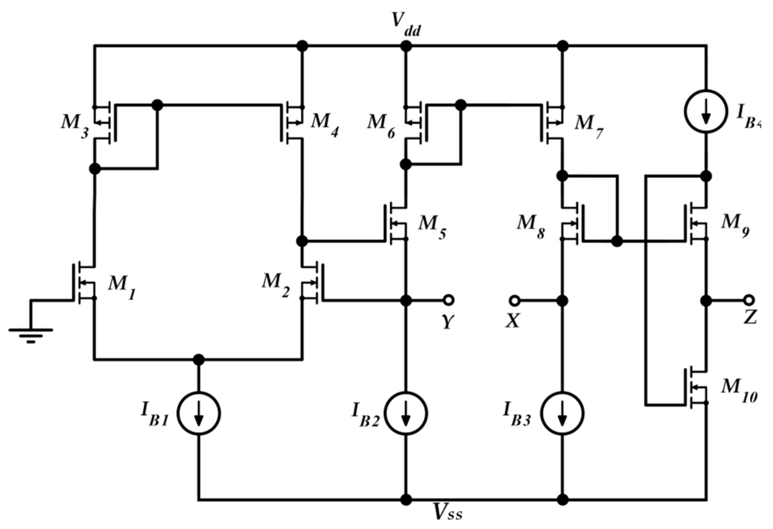
Figure 4.
Mixed circuit and block scheme of the proposed DFVF-VCII-based amplifier.
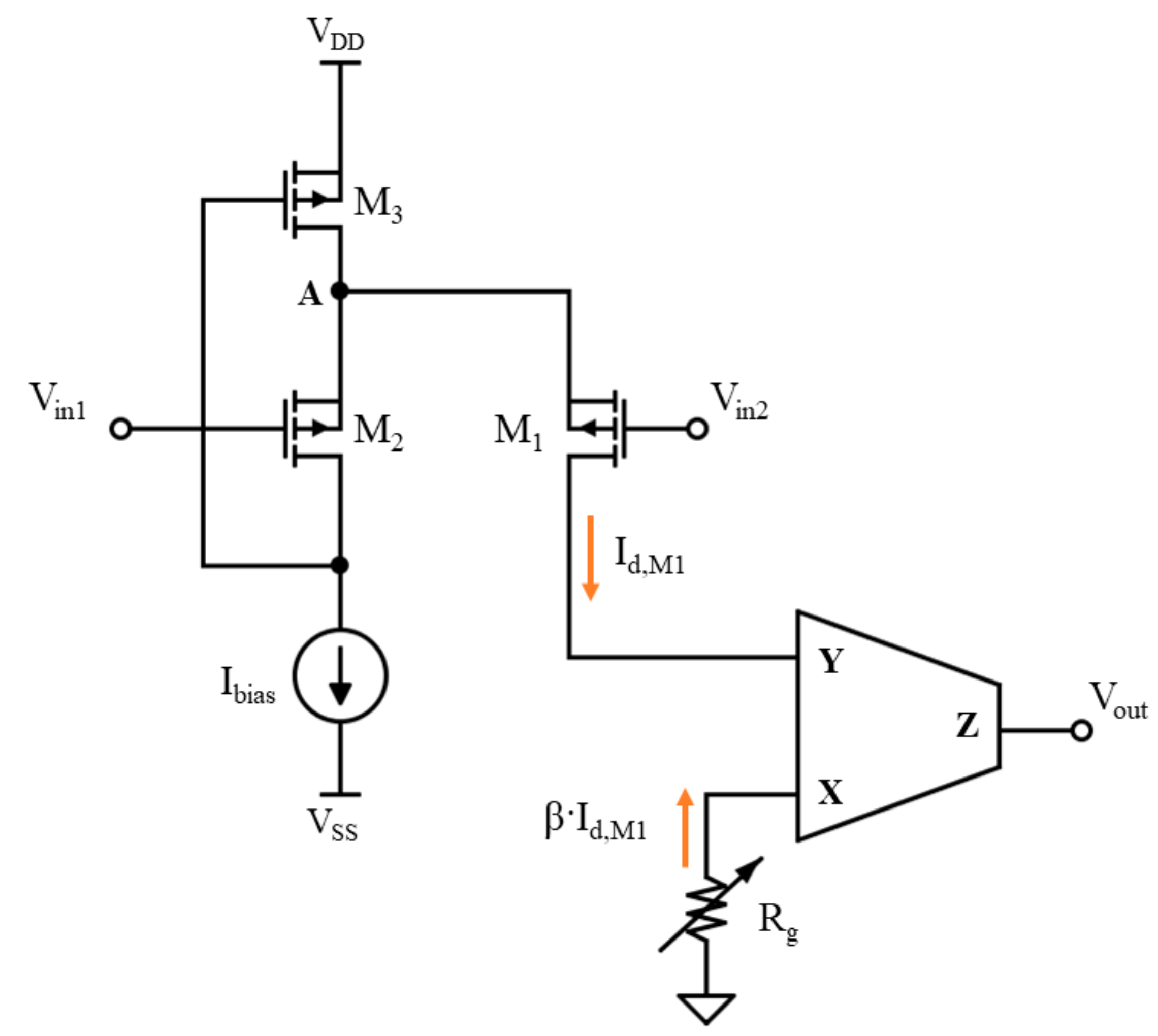
Figure 5.
Implemented PMOS voltage-controlled shunt resistor Rg for neural amplifier gain tuning (a) circuit; (b) resistance vs. control voltage relationship.
Figure 5.
Implemented PMOS voltage-controlled shunt resistor Rg for neural amplifier gain tuning (a) circuit; (b) resistance vs. control voltage relationship.
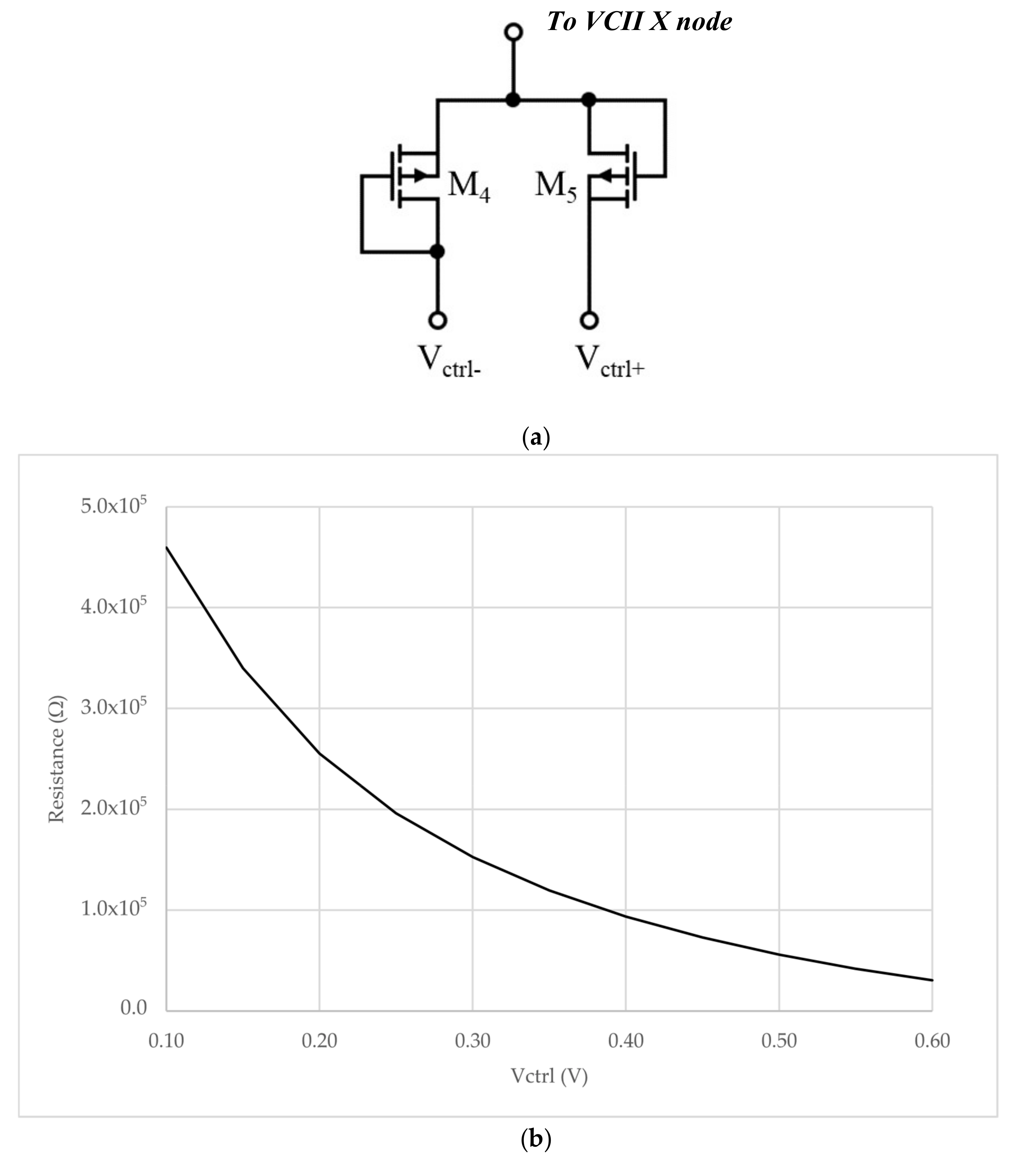
Figure 6.
The complete transistor-level architecture of the proposed neural amplifier. The four main blocks have been highlighted: (1) Biasing current mirror (2) VCII complete block, (3) DFVF standalone block, (4) Voltage Controlled Resistor (VCR).
Figure 6.
The complete transistor-level architecture of the proposed neural amplifier. The four main blocks have been highlighted: (1) Biasing current mirror (2) VCII complete block, (3) DFVF standalone block, (4) Voltage Controlled Resistor (VCR).
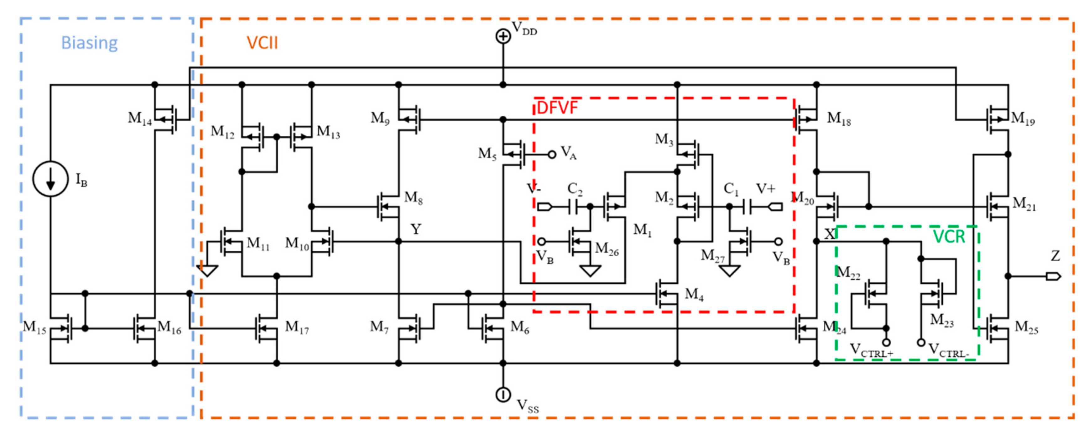
Figure 7.
DFVF differential input voltage vs. output current relationship.

Figure 8.
AC performances of the amplifier at various gain levels.
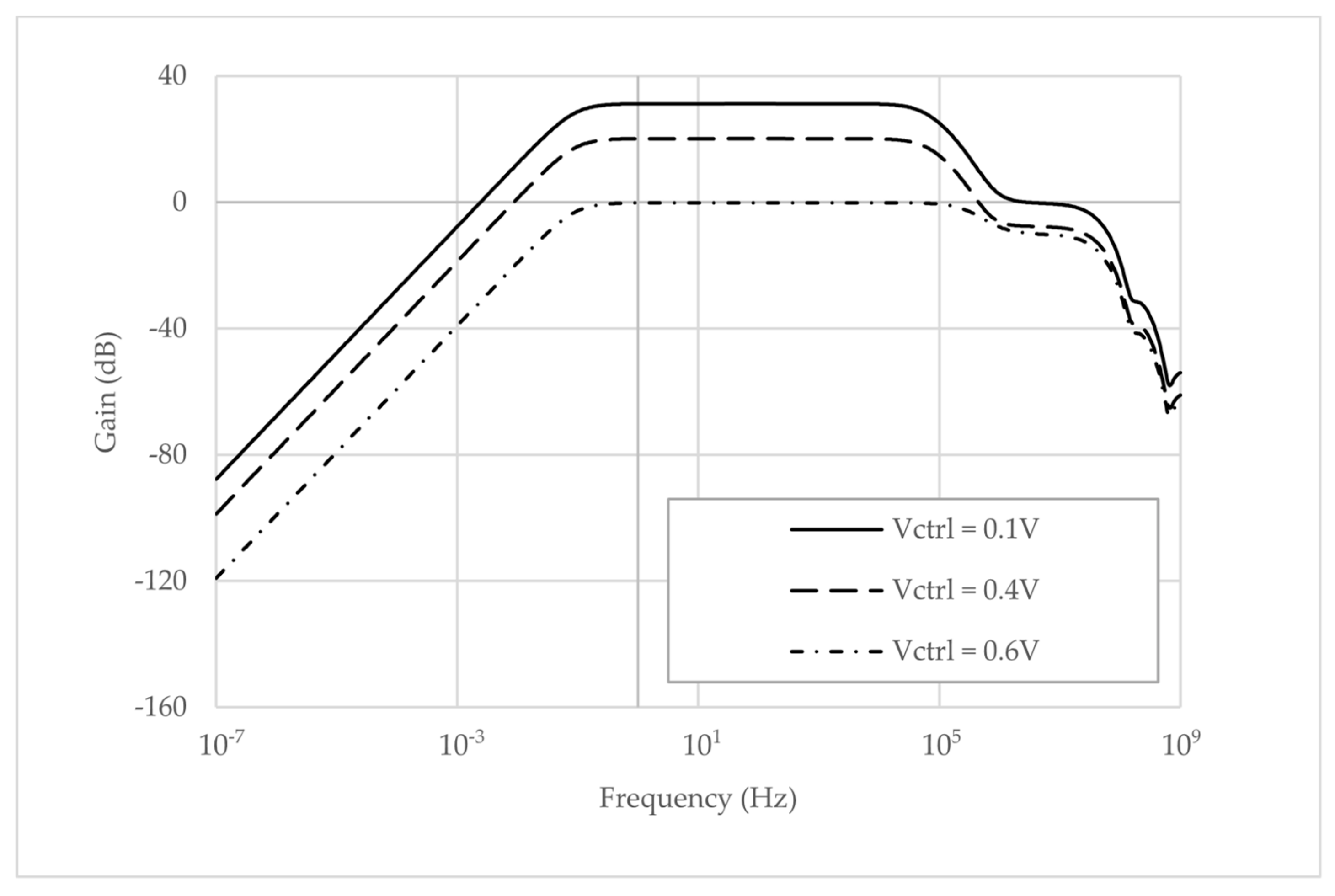
Figure 9.
DC performances of the amplifier at various gain levels.
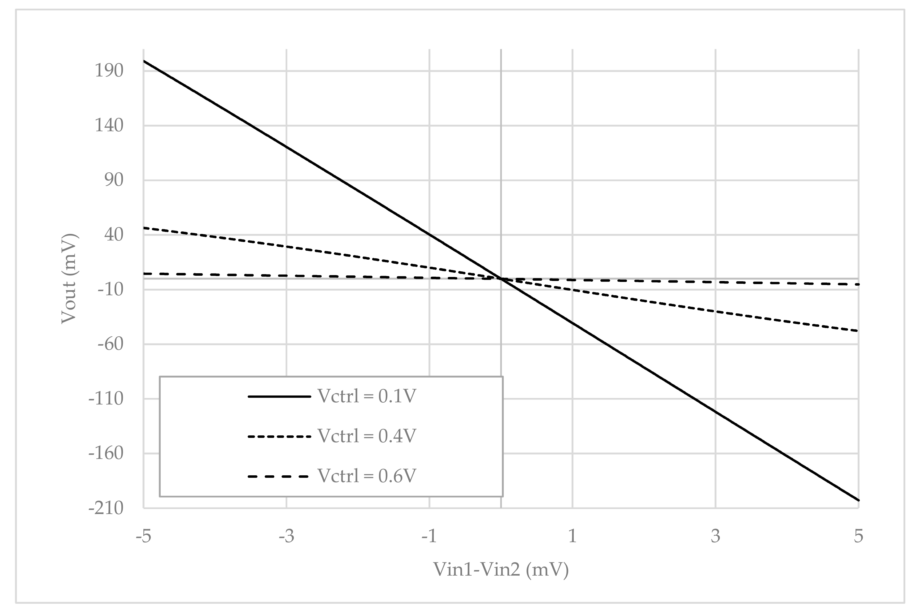
Figure 10.
Input-referred noise performance of the amplifier.
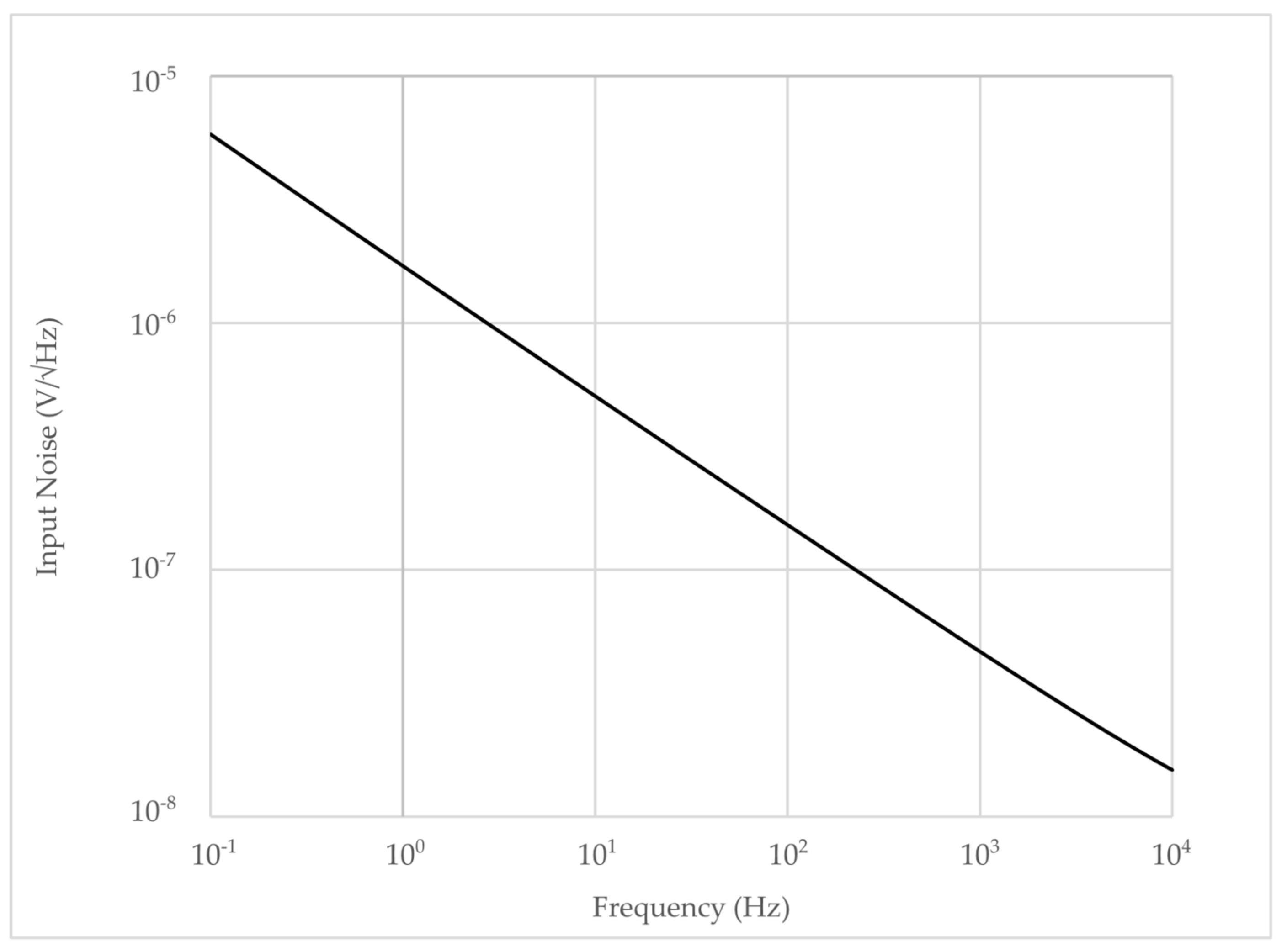
Figure 11.
Input impedance of the proposed amplifier.
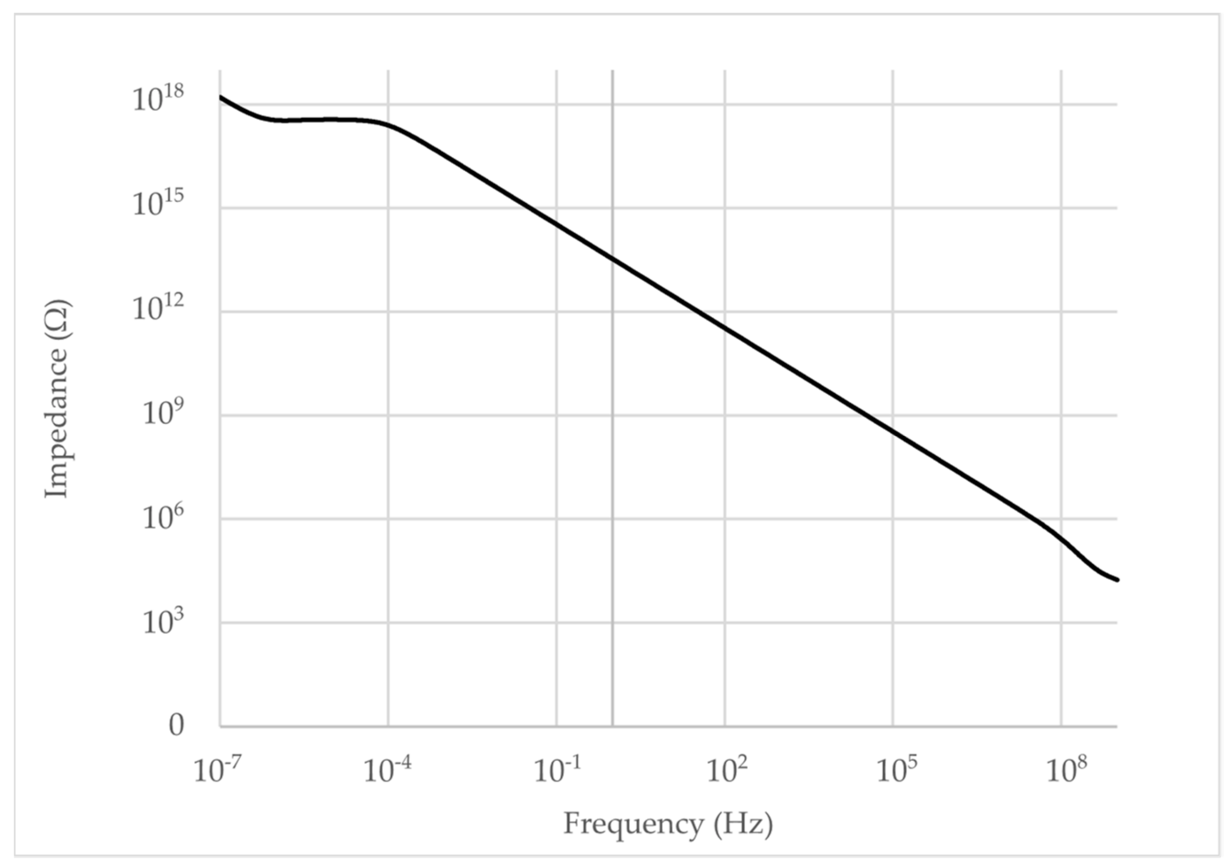
Figure 12.
Statistical distribution of (a) the output voltage, (b) the lower cutoff frequency, (c) the higher cutoff frequency, evaluated under random PVT conditions.
Figure 12.
Statistical distribution of (a) the output voltage, (b) the lower cutoff frequency, (c) the higher cutoff frequency, evaluated under random PVT conditions.


Table 1.
Transistor aspect ratios and main parameter values.
| Transistor | Dimensions (W, L) |
|---|---|
| M1,2 | 5.55 µm, 0.3 µm |
| M3 | 1.05 µm, 0.3 µm |
| M4–6–15–16–17 | 1.8 µm, 1.5 µm |
| M5–9–18 | 11.85 µm, 0.3 µm |
| M8 | 60 µm, 0.15 µm |
| M10–11 | 55.95 µm, 0.15 µm |
| M12–13 | 1.95 µm, 0.15 µm |
| M14 | 7.95 µm, 1.5 µm |
| M7–24 | 3.6 µm, 1.5 µm |
| M19 | 16.05 µm, 1.5 µm |
| M20–21 | 70.05 µm, 0.3 µm |
| M22–23 | 55.05 µm, 18 µm |
| M25 | 1.8 µm, 45.9 µm |
| Parameter | Value |
| IB | 2 µA |
| VA | −290 mV |
| C1, C2 | 1 pF |
| VB | 50 mV |
Table 2.
Comparison table.
| Parameter | This work | 2016 [50] | 2018 [51] | 2019 [53] | 2019 [54] | 2018 [55] |
|---|---|---|---|---|---|---|
| CMOS Technology | LFoundry 150 nm | 180 nm | 180 nm | 180 nm | 180 nm | 500 nm |
| Supply voltage | ±0.6 V | 1.2 V | 1 V | 1.2 V | 1.2 V | 3.3 V |
| Static power consumption | 20 µW | 0.9 µW | 0.25 µW | 8.1 µW | 2.48/5.46 µW (AP/LFP) | 28.05 µW |
| Amplifier Gain (dB) | 0~33 (continuous Tuning) | 30/50 | 25.6 | 26/32/35.6 (Selectable) | 40/20 (AP/LFP) | 49.5 (Untunable) |
| fHPF (Hz) | 10-5 | 6.3 | 4 | 0.025/0.25/0.5/1.5/32/65/125/260 | - | 13 |
| fLPF (kHz) | 174~3980 | 0.175 | 10 | 1/11.4/125 | 100/1000 (LFP/AP) | 9.8 |
| Zin | 3.2 GΩ (@10 kHz) | 20 MΩ | 200 MΩ @100 Hz | - | - | - |
| Zout | 1.2 kΩ (@10 kHz) | - | - | - | - | - |
| THD @frequency reference | 1.02% (−39.8 dB) @Vin = 2mVpp, Vctrl = 0 V, 10 kHz) | 0.4%@1mVpp 10 Hz | - | - | - | 1% @ 0.7 mVpp, 10 kHz |
| Noise Voltage (input referred) | 5.4 µVRMS (0.1 Hz ~ 10 kHz) | 2.6 µVRMS (0.5 Hz ~ 400 Hz) | 3.32 µVRMS (250 Hz ~ 10 kHz) | 6.75 µVRMS (0.5~11.4 k, 40 dB) | AP: 3.44 (0.25 k~10 k) LFP: 6.88 (0.025~600) | 1.88 µVRMS (0.03 Hz~11 kHz) |
| NEF | 8.3 | 6.6 | 1.07 | 7.29 | NA | 2.3 |
© 2020 by the authors. Licensee MDPI, Basel, Switzerland. This article is an open access article distributed under the terms and conditions of the Creative Commons Attribution (CC BY) license (http://creativecommons.org/licenses/by/4.0/).
Share and Cite
MDPI and ACS Style
Stornelli, V.; Barile, G.; Leoni, A. A Novel General Purpose Combined DFVF/VCII Based Biomedical Amplifier. Electronics 2020, 9, 331. https://doi.org/10.3390/electronics9020331
AMA Style
Stornelli V, Barile G, Leoni A. A Novel General Purpose Combined DFVF/VCII Based Biomedical Amplifier. Electronics. 2020; 9(2):331. https://doi.org/10.3390/electronics9020331
Chicago/Turabian StyleStornelli, Vincenzo, Gianluca Barile, and Alfiero Leoni. 2020. "A Novel General Purpose Combined DFVF/VCII Based Biomedical Amplifier" Electronics 9, no. 2: 331. https://doi.org/10.3390/electronics9020331
Note that from the first issue of 2016, this journal uses article numbers instead of page numbers. See further details here.