1. Introduction
At present, electromagnetic compatibility has attracted much attention from the science and technology industry. How to eliminate the electromagnetic interference while reaching a balance in signal quality is a difficult challenge facing every electronic researcher. Nowadays, technology has entered the era of Artificial Intelligence (AI) and the Internet of Things (IoT). As the functions performed by electronic products and facilities function are made increasingly complex and diversified, the mitigation of noise interference plays an important role. If the manufacturing process it is not consideration during the design of electronic products unforeseeable conditions can arise. It is possible for the electromagnetic interference to cause dysfunction, and even result in the crash or burnout of the product.
Currently, there is only limited literature that has focused on the problems caused by electromagnetic interference [
1,
2,
3,
4,
5], which is a challenge faced by every single electronics developer. The design of electronic devices is subject to various limitations in the initial stage, which increases the difficulty that arises from reaching a balance between the quality of signal and electromagnetic interference. It is difficult to ensure that the signal is free from distortion and that the noise meets the existing requirements set out by the international electro technical association.
With respect to the test project of high definition multimedia interface (HDMI) electromagnetic interference (EMI), the product can meet the standard in the design stage, but not satisfy the requirements specified for mass production, which forces the production line to be suspended. Even worse, in some cases, it is necessary to redesign the product, which is not desired by the company. Usually this problem arises from the design stage. The engineers fail to give full consideration to the potential impact of electromagnetic interference, and the choice of countermeasure is unavailable. In addition, these problems result from the design flaws and also from the countermeasure selection. In terms of a general EMI verification project, test results are usually restricted to below the regulatory limit of −0 dB, but the error value can exist in the practical measurement. Therefore, it is essential to identify a proper countermeasure for these factors to be avoided.
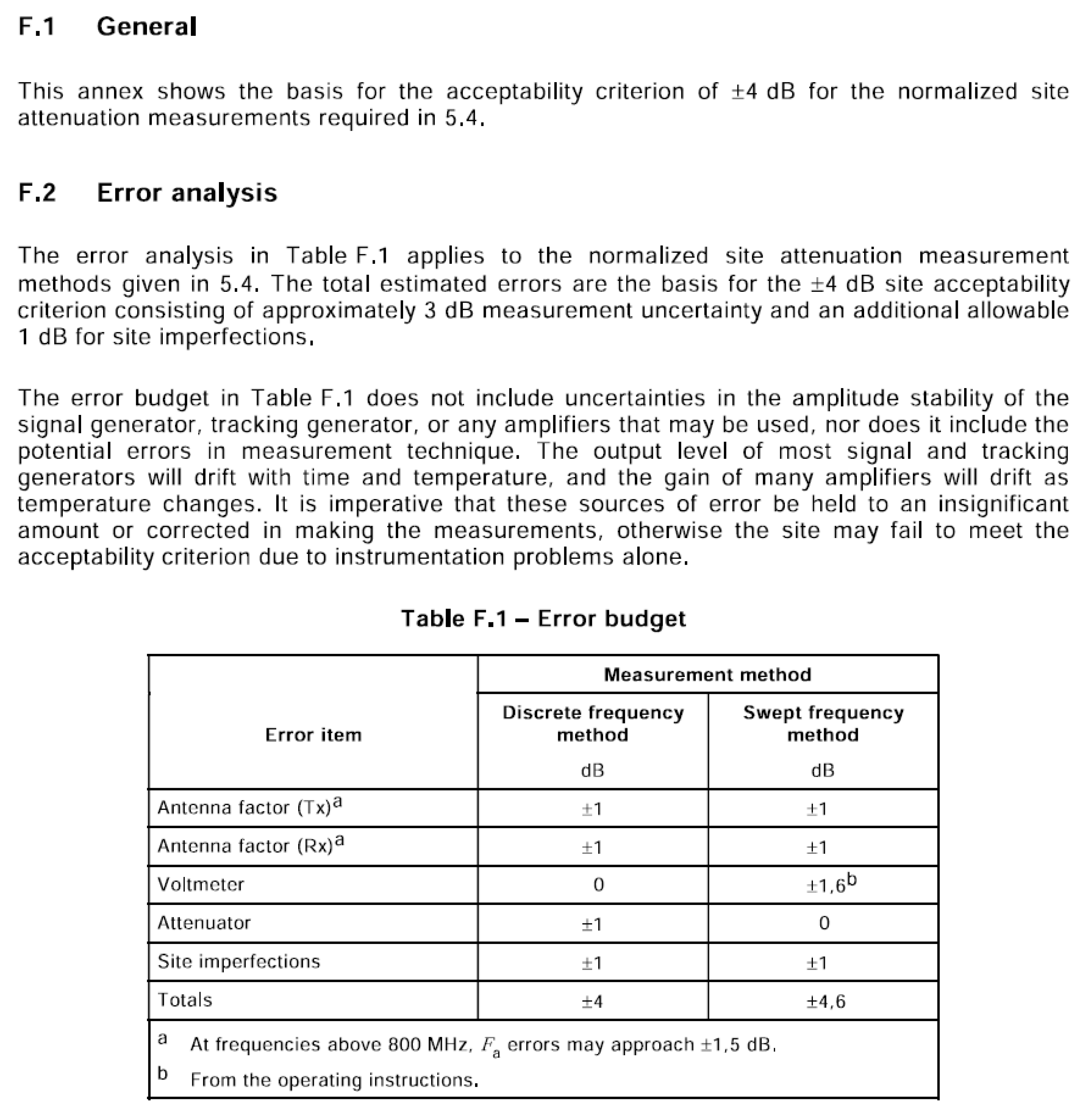
For the general EMI test error, the error value can range between −1 dB and −3 dB. As shown in
Figure 1 [
6], in order to avoid the circumstance where the shipment is affected by a lag in the test schedule as a result of test error, some demanding customers set the verification limitation value below −6 dB at the time of shipment. However, combined with the test errors, as mentioned above, there is a difference of up to 9 dB. Therefore, this is a significant topic for engineers [
7,
8,
9].
With regards to the specifications of HDMI 1.4, its resolution is supposed to support 4K2K with 30 Hz refresh rate. However, according to the verification requirements specified by the customer, HMDI noise at 891 MHz frequency is frequently incapable of meeting the customers’ requirements for EMI of –6 dB, as shown in
Figure 2. * means that the customers’ requirements. The 891 MHz frequency point is merely −2.578 dB. Although the measurement results comply with the EN55022 regulations, they do not conform to the customers’ requirements. Therefore, this paper presents a practical study of a printed circuit board (PCB) layout based on satisfying customers’ requirements for HDMI noise.
2. Theoretical Formulation
During the development of an electronic product, when the electrical engineer or the mechanical engineer lacks the relevant knowledge of electromagnetic compatibility (EMC), a flawed design is unavoidable in the initial research and development stage. The occurrence of electromagnetic radiation during the process of production is not allowed. The most common fatal problem results from the method of wiring.
Generically, when the electronic circuits are designed, electronic engineers take into consideration only signal integrity (SI), power integrity (PI), and impedance matching accuracy (IMA), which means the poor design of conducting wires in PCB is ignored, thus causing an EMI problem. However, most mechanical engineers only give consideration to the stack structure and the minimum line-to-line distance (line length affects price), and therefore overlook whether the wiring and wiring mode crosses in the vicinity of the radio frequency emitting chip, as shown in
Figure 3 and
Figure 4. Invariably, a bad design results in phenomena such as radiation divergence and coupling, either directly or indirectly. In addition, the grounding property of the basic mechanical structure can also be ignored. All these problems contribute to electromagnetic noise. Finally, the EMC measurement results of products are affected. In consideration of this, the relevant issues are worthy of discussion before the design stage in order to prevent serious problems from arising.
Nevertheless, in order to eliminate electromagnetic interference, no more than three elements of electromagnetic interference should be taken into consideration. Although it is unnecessary to address the problem from any aspect at the start, it is recommended to deal with the source of the disturbance at the beginning. An effective design for the wiring can resolve approximately 70% to 80% of the radiation problems. Not only does it reduce the strategy cost incurred by this problem, it also saves a substantial amount of staffing costs related to research and development.
In the general layout of a circuit board (hereinafter referred to as the PCB layout), not only is consideration given to the signal quality and whether the signal function is normal, attention is also given to line width, line spacing, return path, and signal line reference plane. In addition, if the return path is excessively large, the magnetic field effect is produced that creates the EMI radiation area.
In addition, it is necessary to prevent the circumstance where irrelevant through holes pass the high speed or sensitive signal lines. This is because the overly strong noise source makes it easy for signal interference and coupling mechanism to occur, as shown in
Figure 5. For example, regardless of whether a PCB is designed with either four or six layers, if the pulse signal line is shifted from the top layer to the bottom layer, and the pulse signal line is adjacent to the through hole of the high-speed signal line, it is highly likely to cause signal interference. This type of wiring occurs on a frequent basis, which requires developers to pay special attention to this issue.
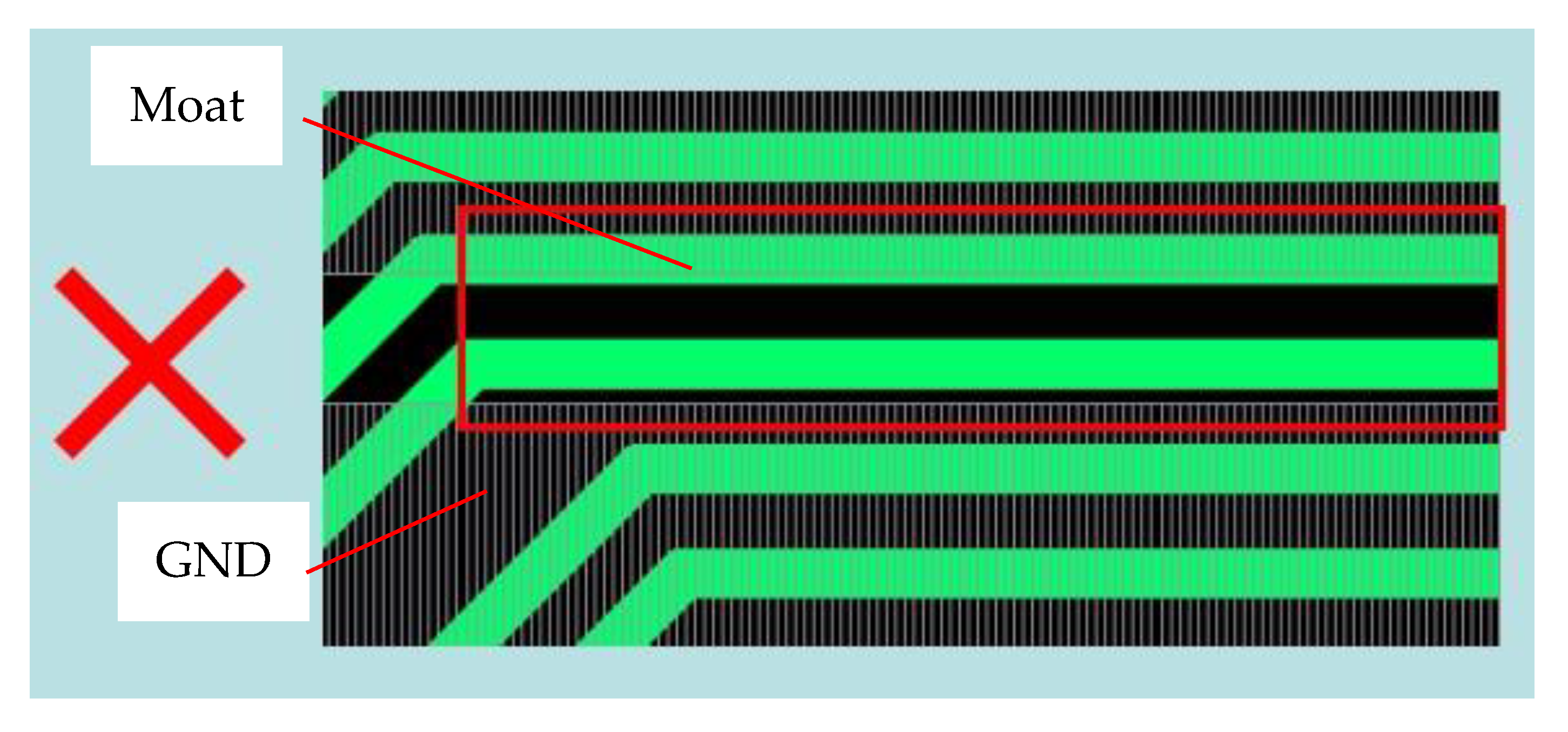
In addition to eliminating the interference of signal line through holes and other signal lines, it is also necessary to take into account the conditions of the return path when the signal lines cannot refer to the same reference plane (GND). In general, a decoupled capacitor is employed, or a reference plane is added to achieve reinforcement by the nearby signal line through hole, as shown in
Figure 6.
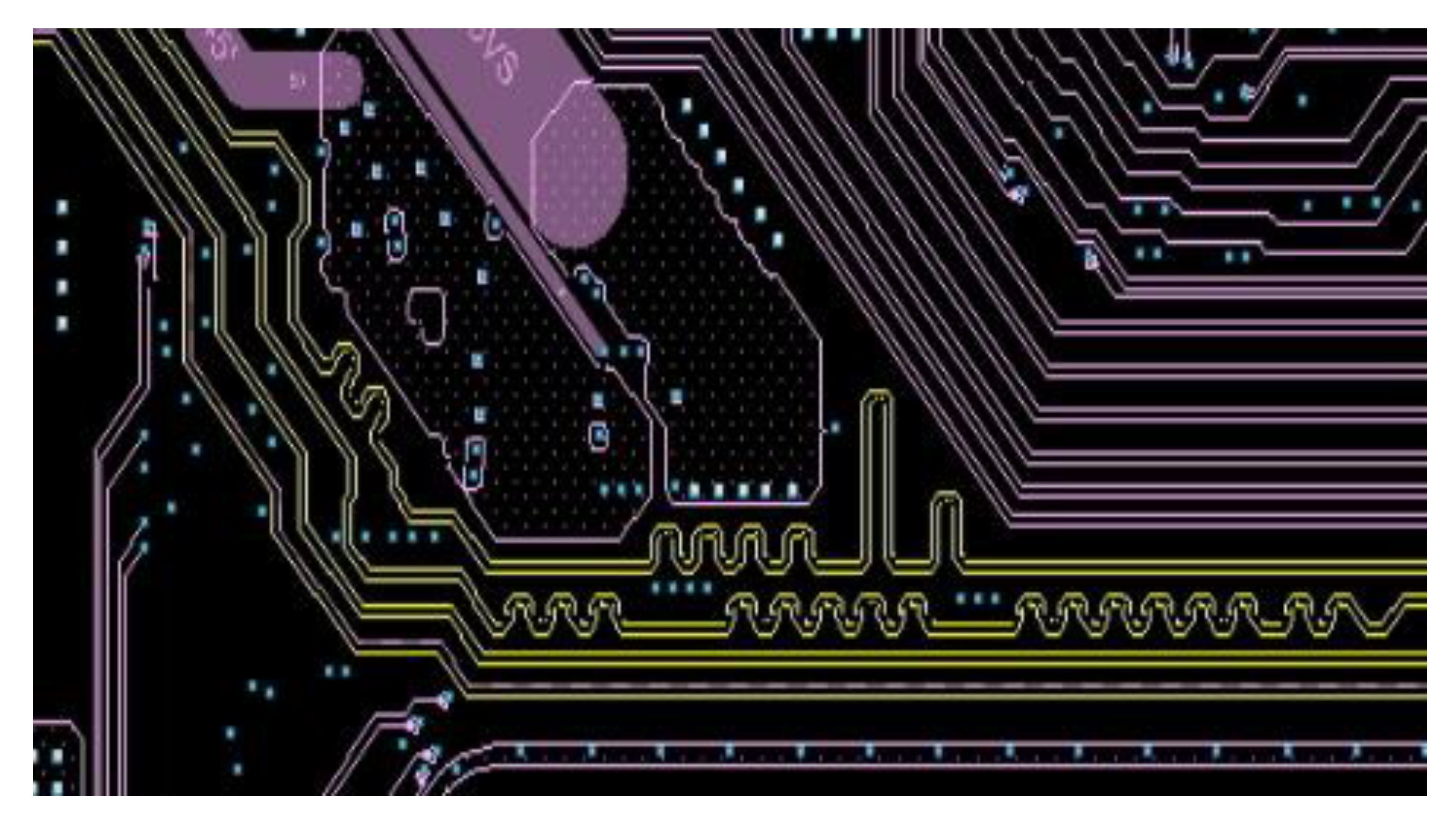
Therefore, it is a necessity that the 3W rule is adhered to as much as possible as part of the wiring requirements [
7]. The clearance between lines should be three times the width of lines, as shown in
Figure 7. It should be measured by midline, or the clearance between lines should be twice as wide as a single line, and snake-like wiring needs to be reduced, as marked in yellow in
Figure 8. In addition, for the signals with high speed and high sensitivity, it is necessary to avoid the clock or the power of the through hole as much as possible. It is also necessary to avoid the front end of the HDMI port and the HDMI signal online. Meanwhile, the PCB factory production line and the line testing point must be detected. If the PCB itself with HDMI signal noise has the opportunity to couple radiation to an HDMI port, what is borrowed from HDMI cable will noise out the screen and join in the high-speed signal transfer layer path GND via design. Moreover, the GND via advice from a signal line shows a penetration hole distance of 25 mil, which makes it necessary not only to shorten the return path and area but also to reduce the formation of the radiation field. These issues affect EMI test results on a frequent basis.
3. EMI Test Environment and Attention
3.1. EMI Validation Environment
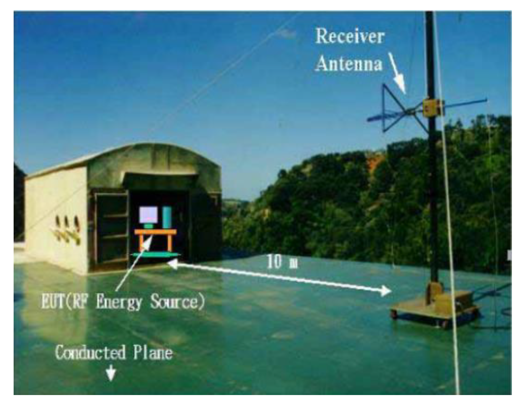
According to the formal EMI EN55022 regulations (30 m~1 GHZ) for validation field, there are two kinds of spaces. One is a relatively open space, commonly known as the open site, as shown in
Figure 9. In some cases, open site testing leads to the results of validation such as the AM/FM radio band in Taiwan from 88 MHZ to 108 MHZ due to the environmental noise effects. If the noise falls into the radio frequency band, the system noise signal is broadcast band and the phenomenon of cover occurs. As a result, the validation gives rise to a grey area, and it is impractical to ensure the authenticity of the products. Due of this, additionally, another indoor dark room space was created, and it is known as the 10 m chamber, as shown in
Figure 10. Since the enclosed space can be isolated from the external noise interference, it ensures that full spectrum noise occurs in electronic products. Although it is not easy to misjudge the noise signal, the venue is costly. Therefore, the chamber has a 10 m fewer third-party certification unit. In addition, to make an appointment at the site, the cost is approximately three to four times higher as compared with the open site.
3.2. EMI Site Configuration Map
In accordance with the regulations set out for an EMI measured erection diagram, as shown in
Figure 11, it is comprised of a pair of conical log periodic antennae. The antenna rises between 1 m and 4 m, while the antenna signal is distinguishable between two vertical and horizontal polarities. It receives the material under test (equipment under test) within 30 MHZ–1 GHZ fan questions around noise. In addition, it locates the EUT ten meters clear of the table and performs the EUT functions. The tunntable is rotated 360 degree, once it receives signals back and forth, to make sure the EUT signals have no dead angles from the antenna. Meanwhile, an examination is carried out on whether the EUT is in compliance with the requirements.
3.3. EMI Verification Attention
During the developmental phase, in order to eliminate errors and the impact of environmental factors, artificial factors should be taken into consideration. When validation issues are considered for the differences in the EUT itself, it is necessary to pay more attention to laboratory space between the measurement error values, and each set up and validation. In general, an engineering personnel certification experimental unit is required to comply with the regulations set out in the standards set.
Every erection is different. Nevertheless, although they are seemingly identical, they are not identical. For example, every time the validation is set u, the first and the second are consistent, and it verifies whether the wire is surrounding the suitability problem. The most common validation that occurs it is the wire surrounding the overlap, as shown in
Figure 12. It is red box space. In some cases, it produces a signal or noise coupling antenna effect, which makes the measurement result far from accurate. If the EMC engineer in research and development validation fails to notice these details, the validation results are inconsistent. A common criticism of the industry is that research and development (R & D) staff need to pay more attention to the erection of validation status to prevent unnecessary problems. In doing so, it ensures that the validation phase results are consistent with mass production.
4. Measurement Data and Experimental Results
In this paper, practicality is introduced to analyze the differences of EMI noise interference countermeasures, as listed in HDMI 1.4 specifications, as follows:
For the discussion and experiment on PCB wiring, this paper mainly focused on examining the distribution of intensity radiation in the near field and EMI results before and after the improvement of HDMI wiring.
Experiment 1 To examine the near field radiation distribution and EMI measurement results of PCB HDMI region;
Experiment 2 To address PCBHDMI noise problem, PCB wiring improvement and measurement of the near field intensity radiation distribution and EMI measurement results are studied.
4.1. HDMI Circuit Diagram and PCB Layout in This Paper
The HDMI circuit diagram, for this paper, is shown in
Figure 13, and the HDMI circuit layout is marked as yellow in
Figure 14.
In order to resolve EMI problems, it is common for EMC engineers to employ the near-field probe to identify the source of PCB noise, in order to reduce cost due to the use of a third-party laboratory for a long time. After identification, the tested objects are transferred to the formal site for verification purposes.
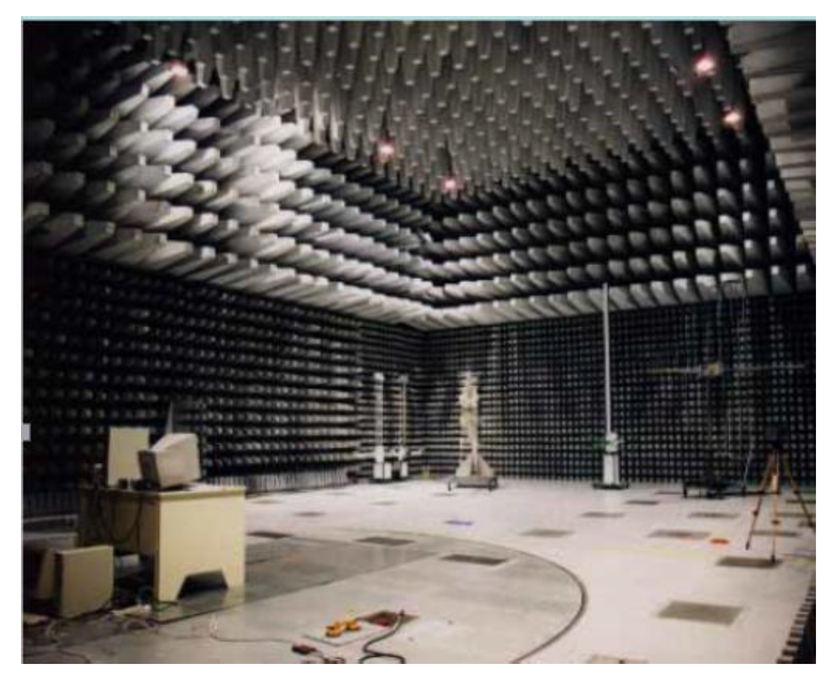
In this paper, APREL EM—ISight was applied to perform the near field measurement, as shown in
Figure 15 [
10]. The instrument relies on mechanical arm instead of hand to hold the receiving antenna (commonly known as the probe). During the process of measurement, the probe will have two directional scannings with a range from 0 degrees to 90 degrees, to simulate the far-field antenna vertical level of polarity, and the area of mechanical arm measurement is set according to the size of the PCB, the displacement of the Probe every time distance, and the minimum moving distance of 1 mm.
4.2. Experiment 1
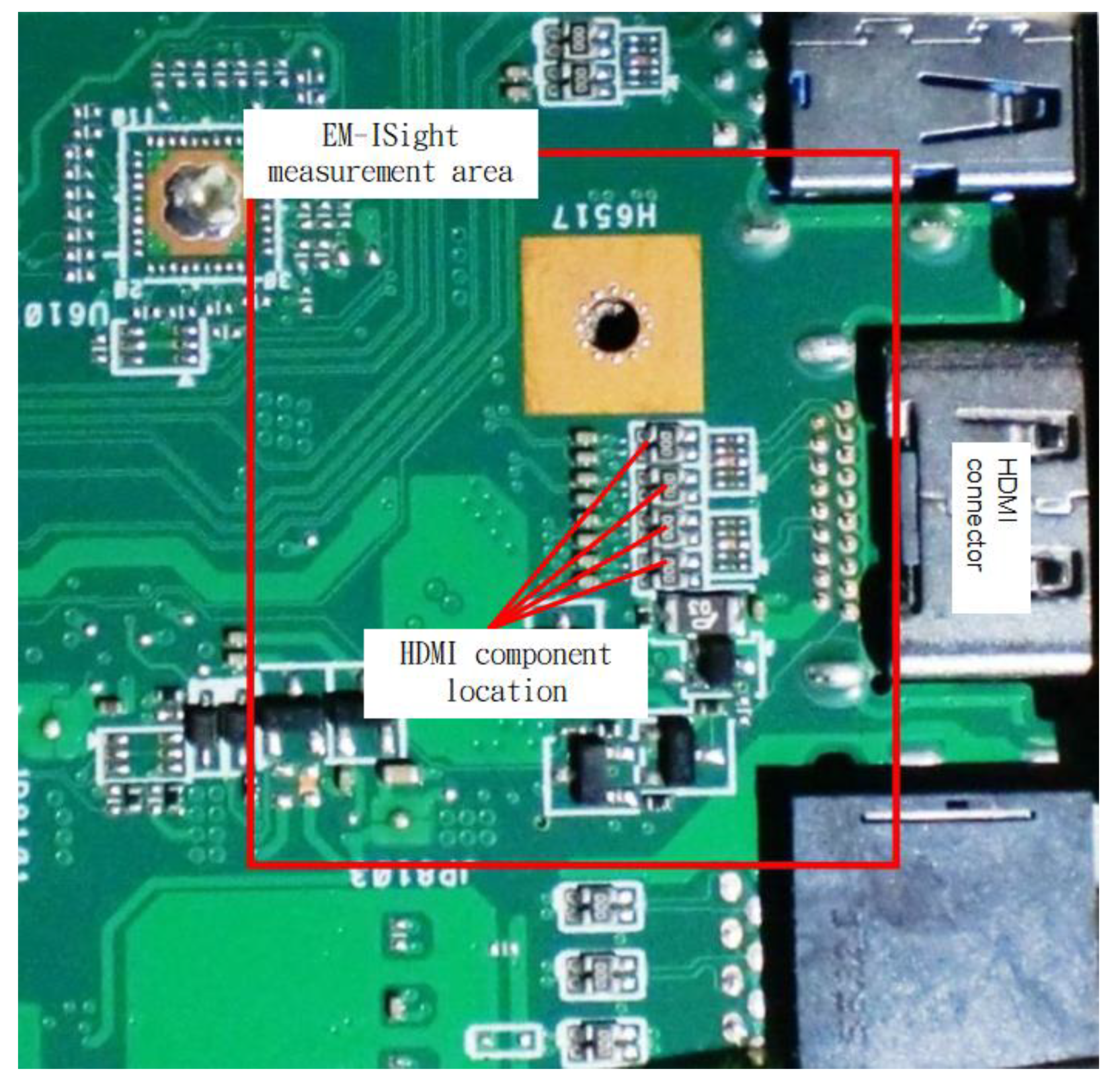
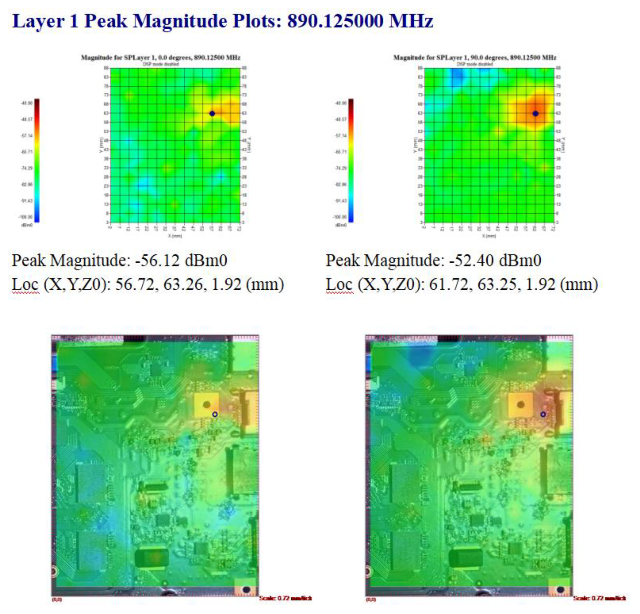
As revealed by the PCB EMI measurement results, the measured spectrum of only HDMI at 297 MHZ and 891 MHZ EMI energy is strong, as shown in
Table 1. While the original design meets the requirements of the laws and regulations, it cannot satisfy the requirements of customers’ demand for a limit of –6 dB. Therefore, the EM—ISight for the near field measurement is applied, and the measurement area is shown in
Figure 15. The red box marks the HDMI, and almost every intensity distribution is shown in
Figure 16.
Before its improvement, the PCB layout for EM—ISight instruments is applied to examine the distribution of recent games intensity to find the HDMI port, and there is also a substantial amount of EMI radiation energy. The scattering region has covered the HDMI and the adjacent IO port (LAN and start), and therefore the noise through the wire around the test is easily out of the noise, as shown in
Figure 16. As for its color, the red represents more energy, and the blue dot in the graph indicates the strongest power in the area.
4.3. Experiment 2
According to the original PCB layout design, we discovered that there is a large number of snaking wires in the HDMI wiring, power supply, and clock via on the side, as well as extra winding, fine tuning, and straightening. In doing so, the bus length can be reduced, and GND can be added at the differential signal wiring change layer. After the improvement of the PCB HDMI layout, the near field measurement area of the HDMI is indicated by the red box, as shown in
Figure 17.
As shown in
Figure 18, in addition to the obvious narrowing of the EMI radiation region, the scattering region also concentrates in the HDMI port, and its energy is not coupled to other ports. In doing so, most EMI problems are resolved. After the improvement of the layout, the EMI measurements conform to the customers’ requirements of −6 db HDMI frequency band points, as shown in
Table 2.
5. Conclusions
In the laptop industry, low levels of profitability and high-quality design are the norm, but it is challenging to ensure design precision and quality while avoiding the waste of cost. We believe this is a difficulty facing each electronic engineer with common HDMI noise as a starting point. In this paper, the following conclusions are drawn:
To resolve the EMC noise problem, first, engineers must clarify and confirm the core of the problem and these problems can be analyzed from three aspects, which are institutional structure, hardware design, and software design;
PCB wiring plays a significant role in hardware design. A good PCB layout is effective in reducing the interference of EMI noise radiation or EMS.
In this paper, an APREL EM-Isight near field detection instrument is applied to assist in analyzing the distribution of electromagnetic noise intensity in the near-field. After verification, the PCB wiring proves to be compliant with the specification after adjustments made to the design, and with the EMI requirements for most HD multimedia interface related products.


