Article

Droplet-Assisted Laser Direct Nanoscale Writing on Silicon †

1
Department of Mechanical Engineering, National Yunlin University of Science and Technology, Douliou, Yunlin 640, Taiwan
2
Department of Mechanical Engineering, National Taipei University of Technology, Taipei 106, Taiwan
*
Author to whom correspondence should be addressed.
This is an extended version of conference paper published in IEEE-NEMS 2014.
These authors contributed equally to this work.
Technologies 2016, 4(1), 8; https://doi.org/10.3390/technologies4010008
Submission received: 31 December 2015 / Revised: 25 January 2016 / Accepted: 19 February 2016 / Published: 2 March 2016
(This article belongs to the Special Issue Laser Percussion Drilling Technology)

Abstract

:
Nano-structuring using laser direct writing technology has shown great potential for industrial applications. A novel application of water droplets to this technology is proposed in this paper. With a hydrophobic layer and a controlled substrate temperature, a layer of randomly distributed water droplets with a high contact angle is formed on the substrate. These liquid droplets can be used as lenses to enhance the laser intensity at the bottom of the droplets. As a result, nanoscale holes can be fabricated on the substrate by controlling the laser energy density. We successfully fabricated holes with a diameter of 600 nm at a substrate temperature of 12 C and a power density of 1.2 × 10⁸ W/cm2 in our experiments. We also found that the hole diameter was around a ninth of the water droplet diameter. Meanwhile, the machined holes are not affected much by the focal length of the lens, but a hole with less than 100 nm in diameter at the center was observed.

1. Introduction

Nanoscale manufacturing technology has been widely applied in the areas of integrated circuits [1], hard disks [2], flexible electronics [3], and optoelectronics [4,5]. However, the cost of conventional optical nanolithography is extremely high. The next-generation nanofabrication techniques still have disadvantages, such as the low throughput of e-beam lithography, and the reliance of the mold fabrication of nanoimprinting on conventional nanolithography. One laser direct writing nanolithography technology is achieved by near-field optics, and three major methods have been developed recently. Laser nanolithography uses a semiconductor, metallic nanoparticles, or a tip-based microscope to enhance the laser intensity directly beneath the particles or tips [6]; however, they have their own technical barriers. In tip-based near-field laser nanolithography, the tip is easily damaged [7], and the throughput is still low [8]. By applying micro/nanoscale spherical particles, the flexibility of the pattern design is limited and the particles are one-time use only. Although different incident angles of the laser increase the time of use of each micro/nanoparticle, the reliability and the uniformity still need to be improved [9,10]. Another method to apply near-field laser direct writing lithography is optical trapping technology, in which particles are moved around on the surface of the substrates [11,12]. The lifetime of the particles is extended by keeping them a tiny distance from the substrate. However, with optical trapping technology, the parallel control of multiple particles is complicated. A novel application of liquid droplets to enhance the laser intensity was investigated in this study. The droplets could be formed and removed easily. Moreover, the droplets instantly cooled down the ablation spots and helped remove the debris during the process. In this study, our intention was to demonstrate the potential of using liquid droplets in laser direct writing nanofabrication. With the condensation of water on silicon in air, the droplets could be randomly distributed on the silicon substrate; therefore, the machined holes were randomly distributed as well. By carefully controlling the laser power density, the debris around the machined holes could be minimized.

2. Principle

The liquid droplet acts as a lens to refract the laser beam, as shown in Figure 1. With a higher refractive index than air, the laser beam is focused onto the substrate. The curvature of the droplet depends on both the contact angle of the droplet, θ, as well as the diameter of the droplet. With a larger curvature, the radius of the beam focused onto the substrate is smaller. In order to minimize the radius of the beam, a larger droplet contact angle and a smaller volume of the droplet are preferable. When the laser beam is focused onto the substrate, laser ablation occurs if the energy density reaches the threshold ablation energy density of the silicon. Taking advantage of the Gaussian distribution of a laser beam, the threshold energy density can be adjusted to be reached in a small area at the center part of the laser beam. Thereby, a nanoscale silicon hole by laser ablation is obtained.

3. Materials and Methods

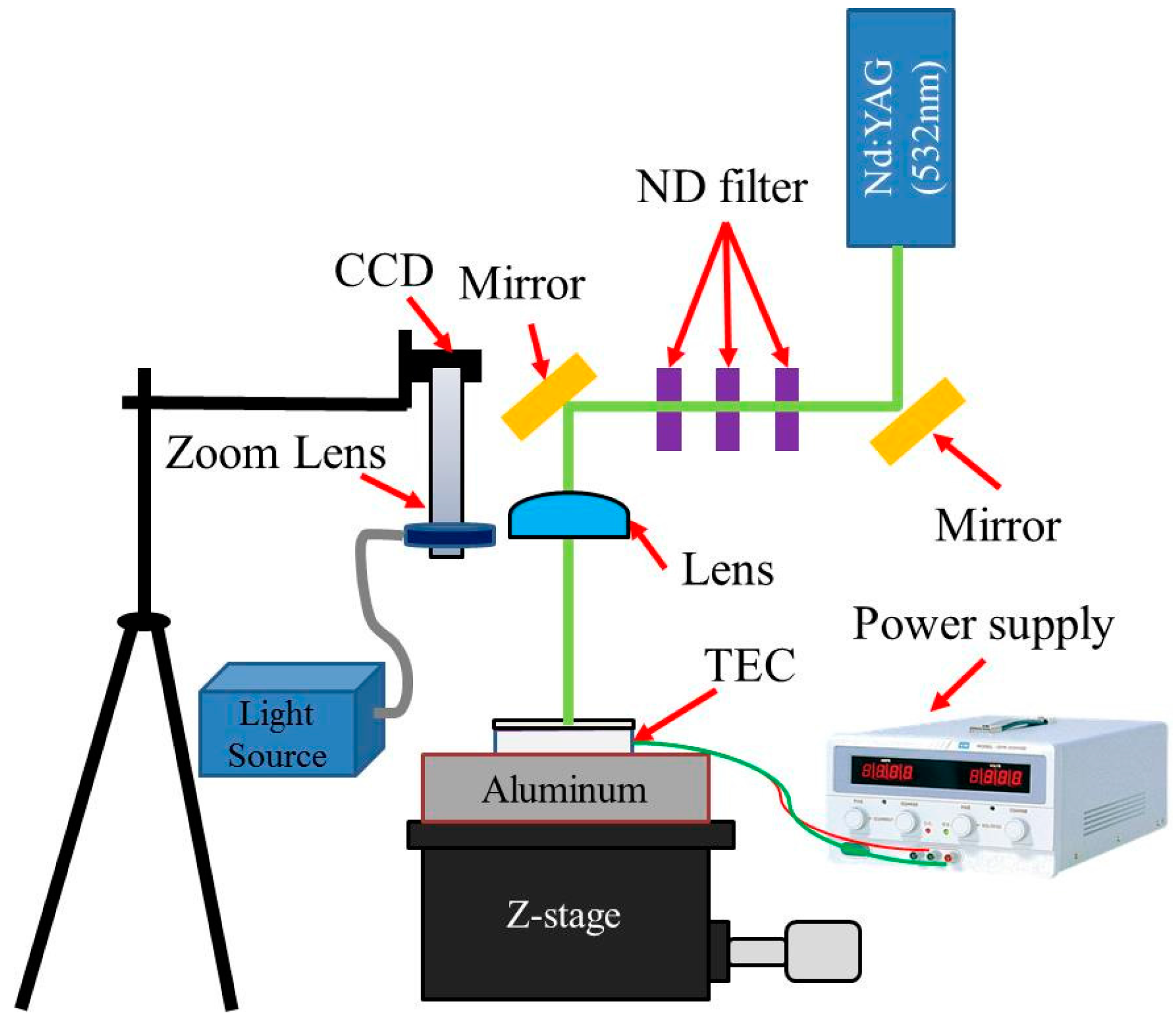
A schematic of the experimental setup is shown in Figure 2. Silicon (Hsin-Chu, Taiwan) coated with a hydrophobic layer was the substrate for patterning. The hydrophobic layer, 1H-1H-2H-2H-Perfluorooctyl-trichlorosilane, was deposited on the silicon substrate by vapor deposition. The substrate was then placed on a thermoelectric cooler (TEC), and the temperature of the silicon was manually controlled with a DC power supply. A pulsed Nd-YAG laser (Lotis TII, Japan) with a wavelength of 532 nm was utilized due to the high absorption by silicon [13] and the low absorption by water [14]. The pulse duration was 6 ns while the output beam size was 6.3 mm in diameter. After being reflected by the first mirror, the laser beam passed through three neutral density filters with different optical density (OD) numbers, 0.2, 0.3, and 1.0, in a series. The laser beam was positively defocused with respect to the substrate, i.e. the focal point was above the substrate and the water droplets. The focal length of the lens was 83.8 mm. The TEC and the silicon substrate were placed on a block of aluminum with a thin layer of thermal paste for heat dissipation. The whole setup was then placed on the stage of a Sodick AP1L Micro Precision Electrical Dischage Machining (EDM) machine (Sodick, Japan). A zoom lens with a charge-coupled device (CCD) was set to take an in situ image of droplets while the silicon substrate was cooling. The image was taken first, and the substrate was moved to the designated position under the lens within 6 s afterwards. A picture of the setup is shown in Figure 3.

4. Results and Discussion

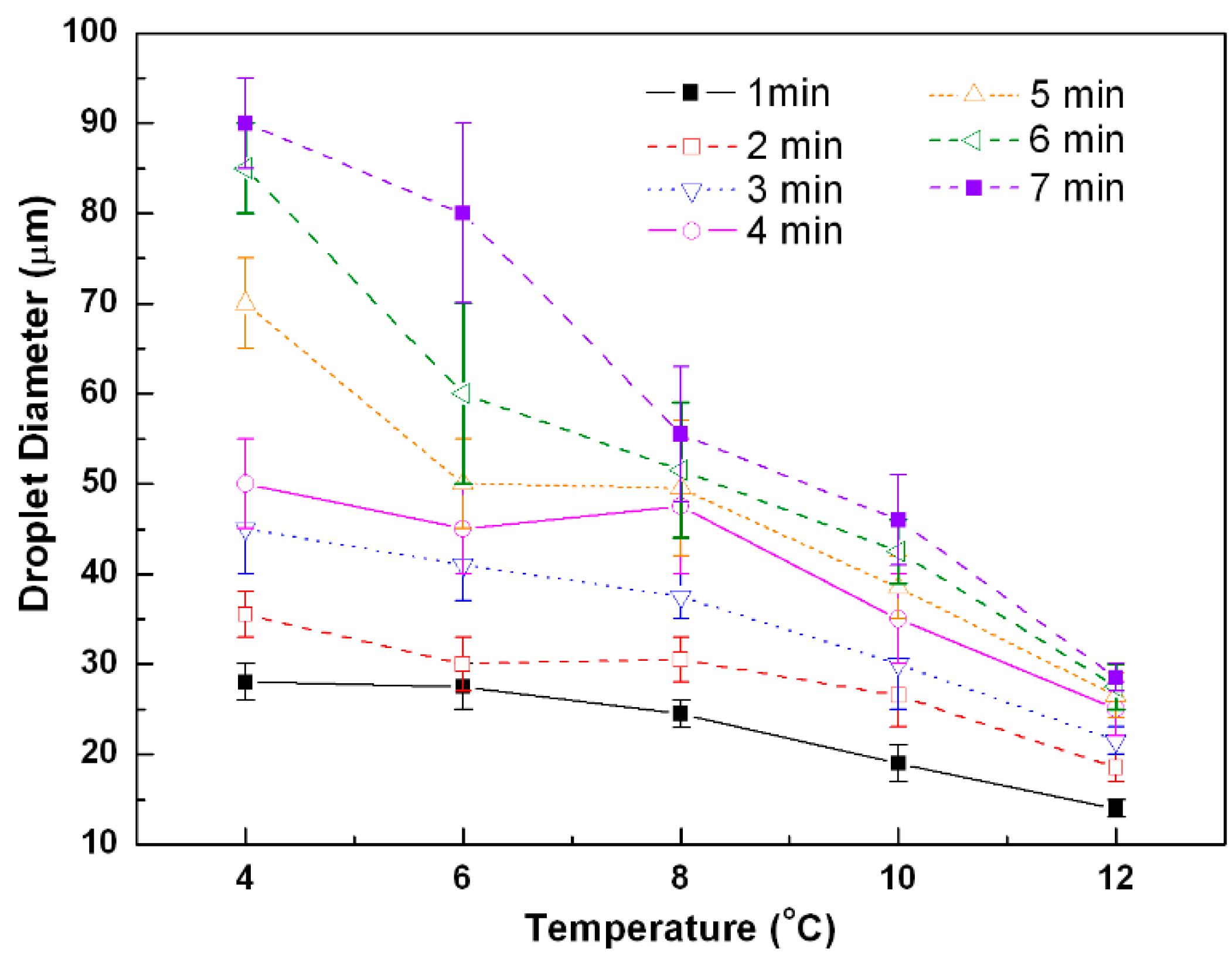
When the substrate temperature was below 12 C, the water droplets were randomly condensed on the silicon, while the relative humidity was in the normal range of 55% to 45%. We measured the size of droplets from 1 to 7 min after reaching the designated substrate temperature. The observed results are shown in 
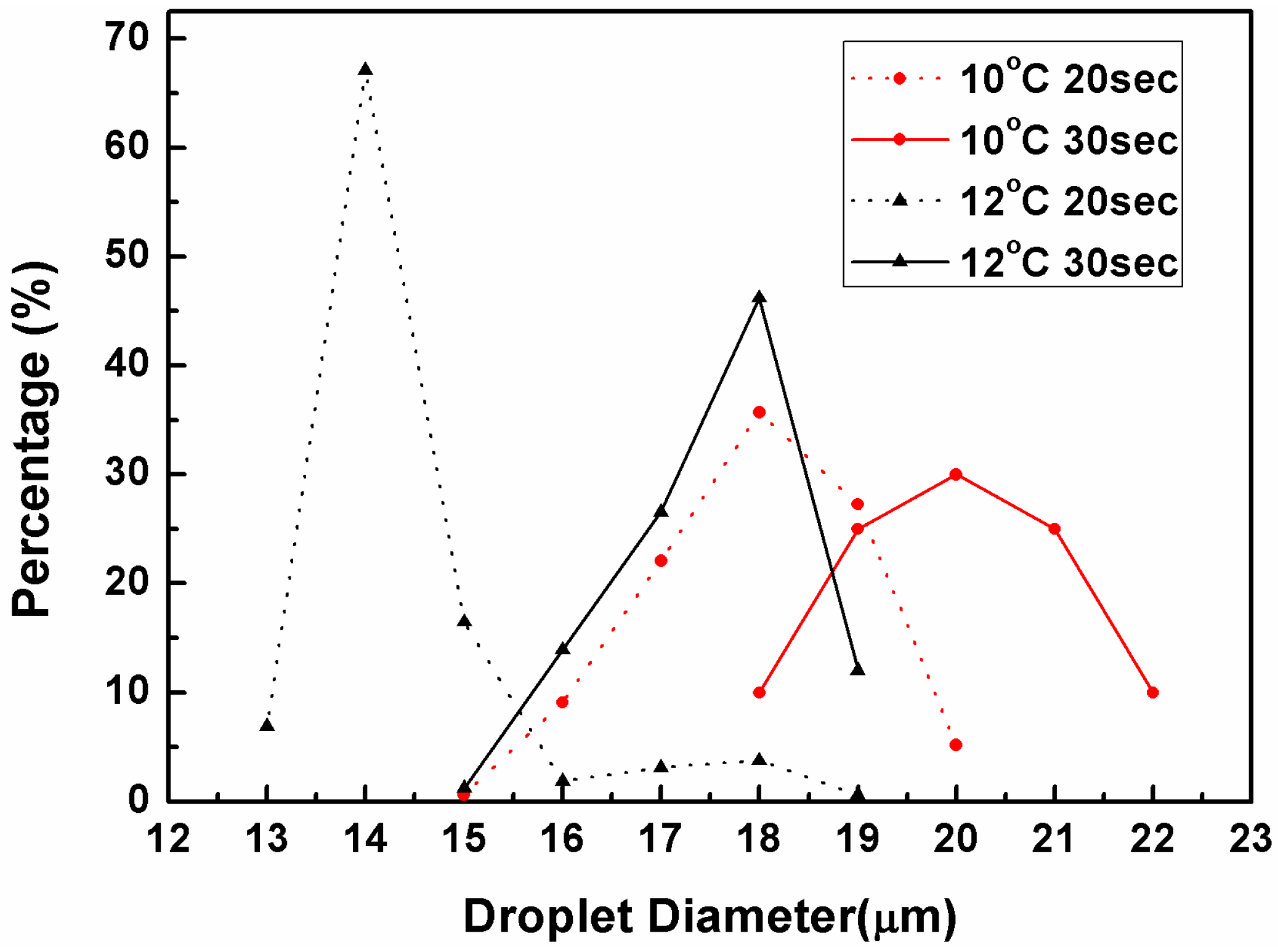
Figure 4. The size of the droplets increased with time and decreased with temperature. We further reduced the condensation time to 20 s and 30 s at both 10 C and 12 C. A picture of the condensed water droplets distributed randomly on the silicon is shown in Figure 5. The diameter in pixels was measured manually for each droplet with the scale bar for obtaining size distribution, as shown in Figure 6. Five different positions on the substrate were measured, including the center and the four corners of the substrate. The droplet diameter distributions are shown in Figure 7. The range of the droplet diameter was 13 μm to 22 μm, depending on the temperature and the condensing time. The variation in diameter at each temperature was around 4 μm. The results also showed that the droplet diameter distribution at 10 C for 30 s was similar to that at 12 C for 20 s. The contact angle of the droplet on the hydrophobic surface was measured to be ~126° by a contact angle analyzer (Phoenix 150, SEO, Korea), as shown in Figure 8.
The laser radiation power after passing through the neutral density filters was 41 mW, with a pumping energy of 23 Joules. Four different power densities were used in our experiments: 1.9 × 10⁸, 1.6 × 10⁸, 1.4 × 10⁸, and 1.2 × 10⁸ W/cm2, and were achieved by adjusting the defocusing distance. The scanning electron microscope (SEM) pictures of the machined holes at different power densities with a substrate temperature of 12 C are shown in Figure 9. From the pictures, we found that the machined area was increased with laser intensity. It can be seen that the holes still exist in the lower left part of the machined area with the lowest power density. This indicates the power density distribution in the laser beam. Higher laser intensity produced the melted silicon sputtered around the hole, while lower laser intensity fabricated circular melting zones, as shown in Figure 9. In Figure 9a, different shapes of holes represent the local power density distribution of the laser beam. With the lowest power density of 1.2 × 10⁸ W/cm2 in our experiments, it can be seen in an enlarged image of Figure 9d that the hole shapes were all circular with less silicon debris surrounding the holes, as shown in Figure 10. With the local power density slightly over the silicon damage threshold, the minimum hole size could be obtained.
Since the machined holes were all perfectly circular with a power density of 1.2 × 10⁸ W/cm2, we measured the width of the melting area and the diameter of the holes machined at this specific power density. An example of the measured hole is shown in 
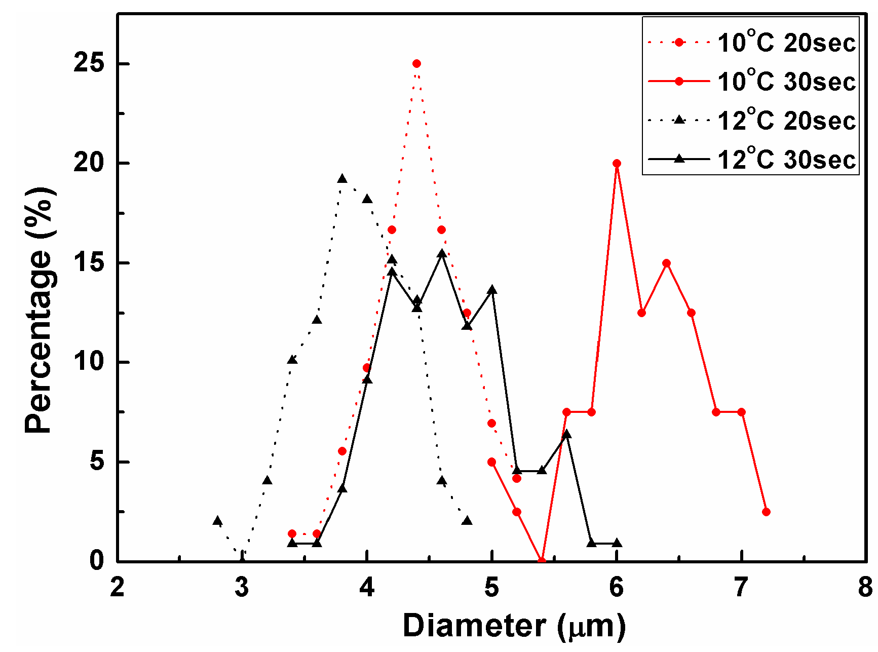
Figure 11. The size distribution of the melting zone and the diameter of the machined holes were measured, and the results are shown in Figure 12 and Figure 13, respectively. The diameter of the melting zone, i.e., the outer diameter of the melting silicon area, was 3 μm to 7.2 μm. The diameter range of the machined hole at the center was 0.6 μm to 4 μm. Lower temperatures and longer condensing times produced larger machined holes. The results also showed that the melting areas of the machined holes were all around 30% of the diameter of the water droplets at the corresponding temperatures and condensation times, as shown in Figure 14. This showed that the power density area in a focused Guassian beam through the liquid lens possibly corresponded to the silicon damage threshold.
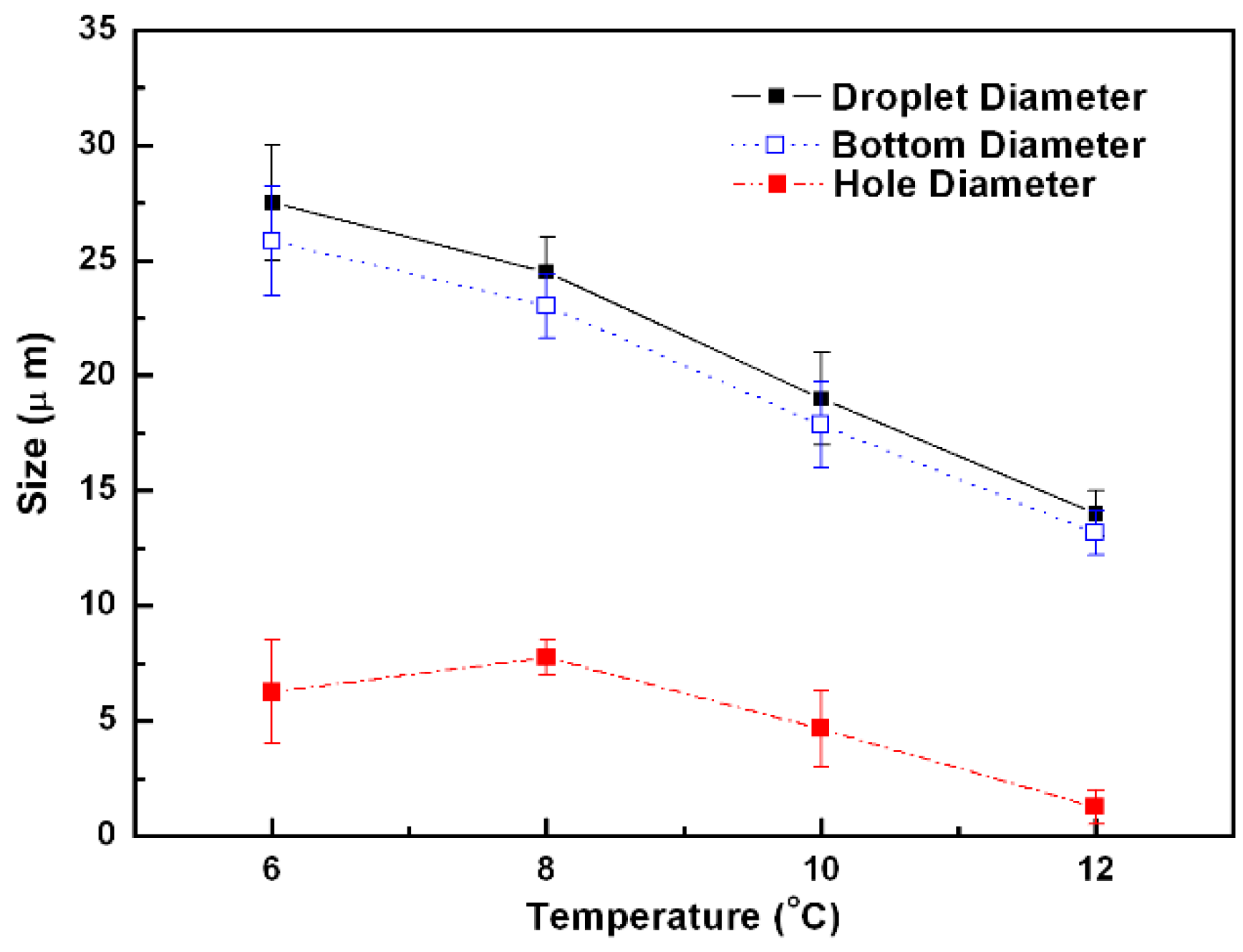
We also compared the hole diameters with water droplet size at different designated temperatures, and the results are shown in Figure 15. The power density was 1.88 × 10⁸ W/cm2. In these experiments, we fabricated the holes on the substrate after 1 min when the designated temperature of silicon was reached. The temperature ranged from 6 C to 12 C. The size of the holes were measured with an SEM. We observed that the higher the substrate temperature that we applied, the smaller the hole diameter that we obtained. The results also show that the smaller droplet size generates smaller holes. Smaller droplets provide larger curvature and results in smaller spot by refraction in the droplet. We also observed that the hole diameters were around a third of the diameter of droplets.
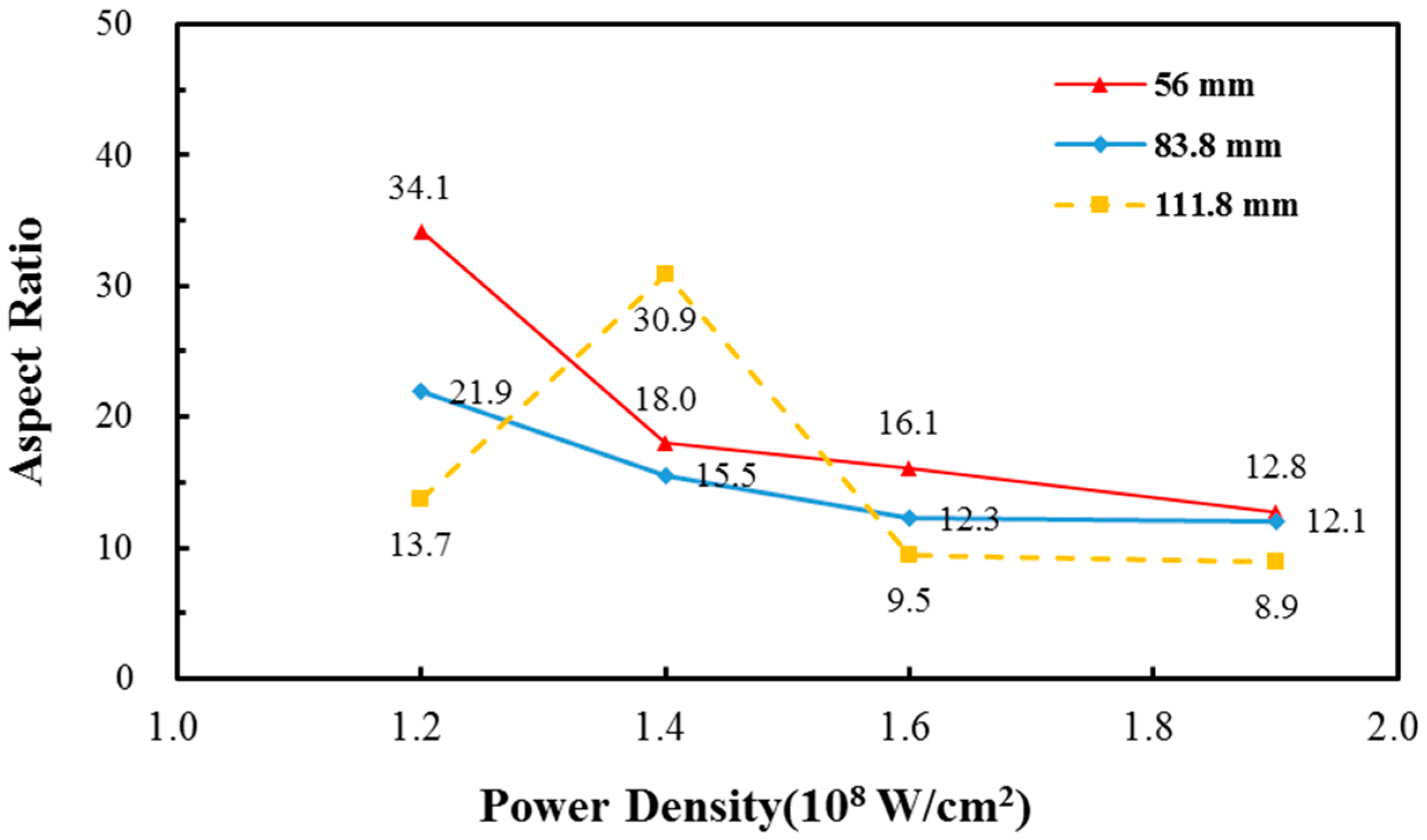
Moreover, we compared the fabricated holes with different focal lengths, including 56 mm, 83.8 mm, and 111.8 mm. The results are shown in Figure 16. The power density used in these experiments was 1.5 × 10⁸ W/cm2. From the SEM pictures, ultra-small holes were found at the center of machined holes. The size of the holes was less than 100 nm. We suggest that it was due to the concentrated energy of a Gaussian laser beam.
We reduced the power density to 1.0 × 10⁸ W/cm2, and the machined holes with different focal lengths are shown in Figure 17. It was clearly found that the ultra-small hole at the center disappeared with the focal lengths of 83.8 mm and 111.8 mm. Only the machined hole with the focal length of 56 mm still has the ultra-small hole at the center. The aspect ratios of machined holes, defined as the ratio of diameter to depth, were measured with these three different lenses and the results are shown in Figure 18. It shows shorter focal length produced holes with higher aspect ratio. Meanwhile, the aspect ratio decreased with the power density. A jump with the focal length of 111.8 mm might be due to the instability of the laser pulse.

5. Conclusions

In conclusion, we have demonstrated that water droplets can be used to achieve laser direct writing nanofabrication. With a droplet diameter of ~13 μm, a hole with a diameter of 600 nm was successfully fabricated at a substrate temperature of 12 C for 20 s. We also found that the hole diameter is around a third of the water droplet diameter. Therefore, smaller droplets produce smaller holes. The machined holes were not affected much by the focal length of the lens, but a hole with less than 100 nm in diameter at the center was observed. The aspect ratio decreased with the power density as well as the focal length of the lens. To reduce the power density further, sub-100 nm holes could possibly be fabricated.

Acknowledgments

The authors would like to thank the National Science Council (NSC102-2221-E-224-015-) for their financial support, and Y.C. Lee’s Lab in the Department of Mechanical Engineering at National Cheng Kung University, Taiwan, for their equipment in supporting the experiments herein.

Author Contributions

Yuan-Jen Chang conceived and designed the experiments; Chao-Hsuan Chang performed the experiments; Chao-Ching Ho, Jin-Chen Hsu and Chia-Lung Kuo analyzed the data; Yuan-Jen Chang wrote the paper. All authors have read and approved the final manuscript.

Conflicts of Interest

The authors declare no conflict of interest.

References

  1. Forrest, S.R. The path to ubiquitous and low-cost organic electronic applications on plastic. Nature 2004, 428, 911–918. [Google Scholar] [CrossRef] [PubMed]
  2. Sbiaa, R.; Piramanayagam, S.N. Patterned Media Towards Nano-bit Magnetic Recoarding: Fabrication and Challenges. Recent Pat. Nanotech. 2007, 1, 29–40. [Google Scholar] [CrossRef]
  3. Jeans, A.; Almanza-Workman, M.; Cobene, R.; Elder, R.; Garcia, R.; Gomez-Pancorbo, F.; Jackson, W.; Jam, M.; Kim, H.-J.; Kwon, O.; et al. Advanceds in roll-to-roll imprint lithography for display applications. Proc. SPIE 2010, 7637. [Google Scholar] [CrossRef]
  4. Madden, S.; Han, T.; Bulla, D.; Davies, B.L. Low loss chalcogenide glass waveguides fabricated by thermal nanoimprint lithography. In Proceedings of Optical Fiber Communication Conference (OFC), San Diego, CA, USA, 11–15 March 2010; pp. 1–3.
  5. Liu, A.; Jones, R.; Liao, L.; Samara-Rubio, D.; Rubin, D.; Cohen, O.; Nicolaescu, R.; Paniccia, M. A high-speed silicon optical modulator based on a metal-oxide-semiconductor capacitor. Nature 2004, 427, 615–618. [Google Scholar] [CrossRef] [PubMed]
  6. Li, L.; Hong, M.; Schmidt, M.; Zhong, M.; Malshe, A.; Huis in’tVeld, B.; Kovalenko, V. Laser nano-manufacturing–State of the art and challenges. CIRP Ann. Manuf. Technol. 2011, 60, 735–755. [Google Scholar] [CrossRef]
  7. Lu, Y.F.; Hu, B.; Mai, Z.H.; Wang, W.J.; Chim, W.K.; Chong, T.C. Laser-scanning probe microscope based nanoprocessing of electronics materials. Jpn. J. Appl. Phys. 2001, 40, 4395–4398. [Google Scholar] [CrossRef]
  8. Murphy-DuBay, N.; Wang, L.; Xu, X. Nanolithography using high transmission nanoscale ridge aperture probe. Appl. Phys. A 2008, 93, 881–884. [Google Scholar] [CrossRef]
  9. Guo, W.; Wang, Z.B.; Li, L.; Whitehead, D.J.; Luk’yanchuk, B.S.; Liu, Z. Near-field laser parallel nanofabrication of arbitrary-shaped patterns. Appl. Phys. Lett. 2007, 90, 243101. [Google Scholar] [CrossRef]
  10. Li, L.; Guo, W.; Wang, Z.B.; Liu, Z.; Whitehead, D.J.; Luk’yanchuk, B.S. Large-area laser nano-texturing with user-defined patterns. J. Micromech. Microeng. 2009, 19, 054002. [Google Scholar] [CrossRef]
  11. McLeod, E.; Arnold, C.B. Subwavelength direct-write nanopatterning using optically trapped microspheres. Nat. Nanotech. 2008, 3, 413–417. [Google Scholar] [CrossRef] [PubMed]
  12. Leitz, K.-H.; Quentin, U.; Alexeev, I.; Schmidt, M. Process investigations of optical trap assisted direct-write microsphere near-field nanostructuring. CIRP Ann. Manf. Technol. 2012, 61, 207–210. [Google Scholar] [CrossRef]
  13. Santbergen, R.; van Zolingen, R.J.C. The absorption factor of crystalline silicon PV cells: A numerical and experimental study. Sol. Energy Mater. Sol. Cells 2008, 92, 432–444. [Google Scholar] [CrossRef]
  14. Pope, R.M.; Fry, E.S. Absorption spectrum (380–700 nm) of pure water. II. integrating cavity measurements. Appl. Opt. 1997, 36, 8710–8723. [Google Scholar] [CrossRef] [PubMed]
Figure 1. Schematic view of laser direct nano-structuring technology.
Technologies 04 00008 g001
Figure 2. Schematic view of the experimental setup.
Technologies 04 00008 g002
Figure 3. Picture of the experimental setup.
Technologies 04 00008 g003
Figure 4. The diameter of droplets on silicon changed with substrate temperature and with the time after reaching the designated temperatures.
Technologies 04 00008 g004
Figure 5. OM picture of condensed water droplet on silicon at 12 C for 20 s.
Technologies 04 00008 g005
Figure 6. Binary image of condensed water droplet on silicon at 12 C for 20 s.
Technologies 04 00008 g006
Figure 7. Size distribution of droplets at 10 C and 12 C.
Technologies 04 00008 g007
Figure 8. Contact angle measurement result.
Technologies 04 00008 g008
Figure 9. SEM pictures of machined holes at different laser power densities (12 C for 20 s).
Technologies 04 00008 g009aTechnologies 04 00008 g009b
Figure 10. Enlarged SEM pictures of machined holes with 12 C for 20 s.
Technologies 04 00008 g010
Figure 11. SEM picture of a machined hole with power density of 1.2 × 10⁸ W/cm2 at 12 C for 20 s.
Technologies 04 00008 g011
Figure 12. Size distribution of melting width of machined holes at 10 C and 12 C with a power density of 1.2 × 10⁸ W/cm2.
Technologies 04 00008 g012
Figure 13. Diameter distribution of machined holes at 10 C and 12 C with a power density of 1.2 × 10⁸ W/cm2.
Technologies 04 00008 g013
Figure 14. Comparison of droplet size, hole diameter and melting diameter of machined holes at 12 C condensing for 30 s.
Technologies 04 00008 g014
Figure 15. Comparisons among droplet diameters, bottom diameters of droplets, and fabricated hole diameters, with the substrate temperature ranging from 6 C to 12 C.
Technologies 04 00008 g015
Figure 16. SEM picture of machined holes with different focal length (scale bar = 5 μm).
Technologies 04 00008 g016
Figure 17. SEM picture of machined holes with a power density of 1.0 × 10⁸ W/cm2 (Scale bar = 5 μm).
Technologies 04 00008 g017
Figure 18. Aspect ratio of holes at different power density with three different focal length.
Technologies 04 00008 g018

