Article

High-Efficiency and Large-Angle Homo-Metagratings for the Near-Infrared Region

1
Department of Photonics, College of Electrical and Computer Engineering, National Yang Ming Chiao Tung University, Hsinchu 30010, Taiwan
2
Semiconductor Research Center, Foxconn Research, Taipei 11492, Taiwan
*
Authors to whom correspondence should be addressed.
Photonics 2024, 11(5), 392; https://doi.org/10.3390/photonics11050392
Submission received: 5 March 2024 / Revised: 18 April 2024 / Accepted: 22 April 2024 / Published: 24 April 2024
(This article belongs to the Special Issue Advanced Lasers and Their Applications)

Abstract

:
Compact photonic devices that integrate metasurfaces with light sources have been widely studied. However, experimental demonstrations of a higher efficiency of integration are still lacking. To enhance the efficiency of light sources integrated with metasurfaces, we employed a forward design optimization method and index matching between the light source and metasurface substrate to design metagratings. To optimize the overall diffraction efficiency, we manipulated the degrees of freedom in phase, the lattice constants, and the number of unit cells. The same material was utilized for the nanostructures and substrate (homo-metagrating) for index matching, while Si and GaAs materials were used for working at 1550 and 940 nm, respectively. The experimental homo-metagratings operating at 1550 nm and made of Si exhibited an overall average efficiency of 51.3% at diffraction angles of 60.3°. On the other hand, experimental homo-metagratings operating at 940 nm and made of GaAs exhibited an overall average efficiency of 52.4% at diffraction angles of 49.3°. This suggests that the future integration of metagratings with a polarization-specific laser can further enhance the overall diffraction efficiency.

1. Introduction

In recent years, the use of metasurfaces as novel optical elements has been extensively discussed [1,2,3,4]. Metasurfaces, being artificial layers, alter the amplitude and phase of incident light, thereby enabling the manipulation of diffraction light to achieve desired functionalities and applications, including in optical vortex generators [5], achromatic lenses [6,7], monolithic spiral metalenses [8], polarization converters [9], Janus metasurfaces [10,11], meta-holograms [12], hyperspectral imaging [13], and facial depth sensing [14]. Due to their lighter weight and smaller volume compared to traditional optical components, metasurfaces have shown the potential to replace conventional optical elements [15]. However, efficiency is a critical issue in these demonstrations, as the efficiency of metasurfaces can serve as an important performance metric for these components.
Numerous studies have been devoted to improving diffraction efficiency. For instance, some researchers utilized isophase streamline optimization methods to design silicon complementary metal–oxide–semiconductor (CMOS) compatible metagratings with nearly 100% diffraction efficiency [16]. Additionally, one study achieved up to 90% diffraction efficiency in the visible light spectrum using kissing-dimer metagratings [17]. Furthermore, another study employed high-refractive-index silicon as the metasurface material, achieving a diffraction efficiency of 71% at a working wavelength of 532 nm [18]. Additionally, topology optimization techniques can be used to design metasurfaces with high diffraction efficiency [19]. However, all of these advancements fall within the realm of hetero-metasurfaces. Considering their integration with light sources, employing homogeneous metasurface interfaces with refractive indices similar to those of the light sources can effectively resolve impedance matching issues between the light source and the metasurface substrate.
Therefore, studies have addressed this issue by integrating GaAs metasurfaces with vertical-cavity surface-emitting lasers (VCSELs) to reduce light loss [20,21,22], achieving an overall efficiency of 40.8% at a diffraction angle of 30° [23]. Considering the materials of the light source (GaAs and InP), we propose utilizing GaAs and crystalline silicon as the materials for metagratings [24]. All the Si materials described hereafter are c-Si. These materials were chosen due to their refractive indices, closely matching those of the source materials. The metagratings are specifically designed for application at wavelengths of 940 nm and 1550 nm, aiming to boost their overall diffraction efficiency. The reason why we are not using InP material is due to the limitations of our fabrication technology. Additionally, since the cost is relatively lower and the fabrication technologies are more mature for Si than for InP, we opted for Si as the material for the metasurface. Discussing high efficiency naturally leads to concerns about potential safety hazards to human eyes. The 1550 nm wavelength offers a significantly higher maximum permissible exposure (MPE) limit compared to 905 nm, approximately one million times greater [25]. In atmospheric conditions, light at 1550 nm experiences less scattering and attenuation compared to that at 905 nm. When light at a wavelength of 1550 nm propagates through the atmosphere, it experiences less interference from ambient light than does that at 905 nm. In the context of humid weather conditions, wavelengths of 1550 nm and 905 nm lie within atmospheric windows where water vapor absorption is comparatively low [26]. This characteristic suggests that light at 1550 nm offers advantages for long-distance transmission applications. Therefore, after completing the homo-metagratings for GaAs, we designed Si homo-metagratings based on the refractive index of the 1550 nm photonic crystal surface-emitting laser (PCSEL) material InP. In commercial applications, Luminar has developed an automotive LiDAR system that utilizes 1550 nm lasers. This system is capable of detecting objects up to 300 m away at night, while ensuring safety for human eyes.
In this paper, we enhance the overall diffraction efficiency of Si and GaAs metagratings through a simple forward design method and by optimizing the degree of freedom (DOF) for the phase. The optical setup for the efficiency measurement of metagratings is illustrated in Figure 1a. In practical measurements, semiconductor lasers are used as the light source for metagratings. The types of lasers can include Fabry–Pérot (FP) lasers, distributed feedback (DFB) lasers, vertical-cavity surface-emitting lasers (VCSELs), and photonic crystal surface-emitting lasers (PCSELs). Two linear polarizers are optimized to generate and analyze the laser’s polarization state (TM or TE) considering the diffraction plane. The definition of polarization is depicted in Figure 1b. When light is incident along the z-axis onto the metagratings, the y–z plane is defined as the diffraction plane. Therefore, the TM and TE polarized light states are defined as the polarization states of light where the electric fields are perpendicular and parallel to the diffraction plane, respectively. The metagrating consists of unit cells arranged in a hexagonal lattice along the y-axis, where each meta-atom can also be referred to as a unit cell.

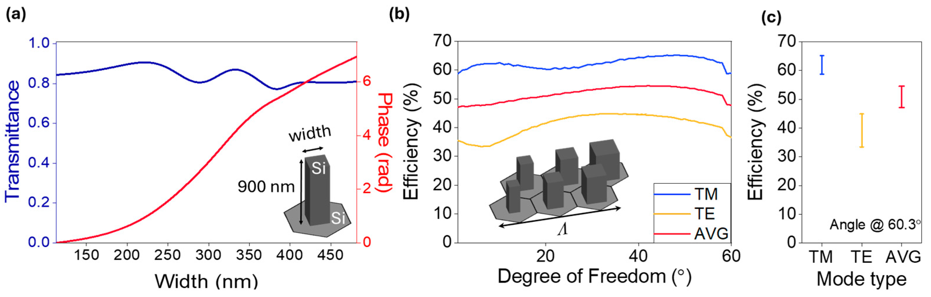
2. Design of Si Metagrating

To verify the transmittance and phase coverage of the unit cells, we utilized the RETICOLO package [27] to calculate the transmittance and phase coverage for nanopillars with various geometric parameters. Both the simulated nanopillars and the substrate were Si. Figure 2a illustrates a square nanopillar (unit cell) with a fixed height of 900 nm, showing the function of its width variation at a working wavelength of 1550 nm. The lattice constant of the unit cell was 595 nm. In our simulated unit cells, the lattice constant was not limited to 595 nm but ranged from 500 to 690 nanometers. Considering the limitations of sample fabrication, we simulated a set of Si unit cells with widths from 113 nm (for which the aspect ratio of the nanopillars’ width to their height is 8) to 495 nm (the lattice constant of the unit cell minus 100 nm) to analyze their transmittance and phase coverage. When the phase coverage of the unit cells exceeds 2π, phase shifting can be utilized to find nanopillars of different widths (degree of freedom for the phase) that maintain the same phase.
Figure 2b illustrates the optimization of the diffraction efficiency (Tm) with the DOF for the phase, ranging from 0 to 60°. The diffraction efficiency is most often defined in simulations as the light power ratio between the ideal order of beam deflection and that in the substrate [24]. We can see that the efficiency changes with different DOFs. The ideal phase distribution of the metagratings accompanying the DOF is defined as
Φ d e f l e c t o r ( x ) = 2 π λ x sin θ + δ ,
where δ is a constant relative to the position, which can be any value and can be considered as the degree of freedom for the phase. The diffraction angle (θ) is defined as
θ = sin 1 λ Λ = sin 1 λ N × U × n t
Here, U is the lattice constant (unit cell size) of the meta-atom and N refers to the number of cells arranged along the diffraction angle direction, appearing in a hexagonal lattice arrangement. In our previous article, we compared the diffraction efficiency of metagratings arranged in hexagonal and square lattice configurations [24]. We chose to focus on the hexagonal lattice arrangement for the meta-atoms because our simulations showed that it generally provided higher diffraction efficiency compared to the conventional square lattice for most cases [24]. However, we did observe a few instances where the square lattice showed higher efficiency. The choice of lattice ultimately depends on the specific design requirements and optimization goals of the metagrating application. U denotes the lattice constant of the unit cell, while nt is the refractive index of the medium through which light propagates after traversing the metasurface. The inset of Figure 2b shows a supercell, with its periodicity defined as Λ = N × U. In the example in Figure 2b, the number of unit cells (N) within a supercell is 3, the lattice constant is 595 nm, and the corresponding diffraction angle is 60.3°. This approach provides the ability to find the efficiency range and maximum efficiency for TE, TM, and their average, as shown in Figure 2c. For example, we selected a DOF of the phase of 42° for the highest average efficiency. Additionally, the widths of the nanopillars within the metagratings were 207, 258, 294, 327, 358, and 408 nm.

3. Fabrication of Metagratings

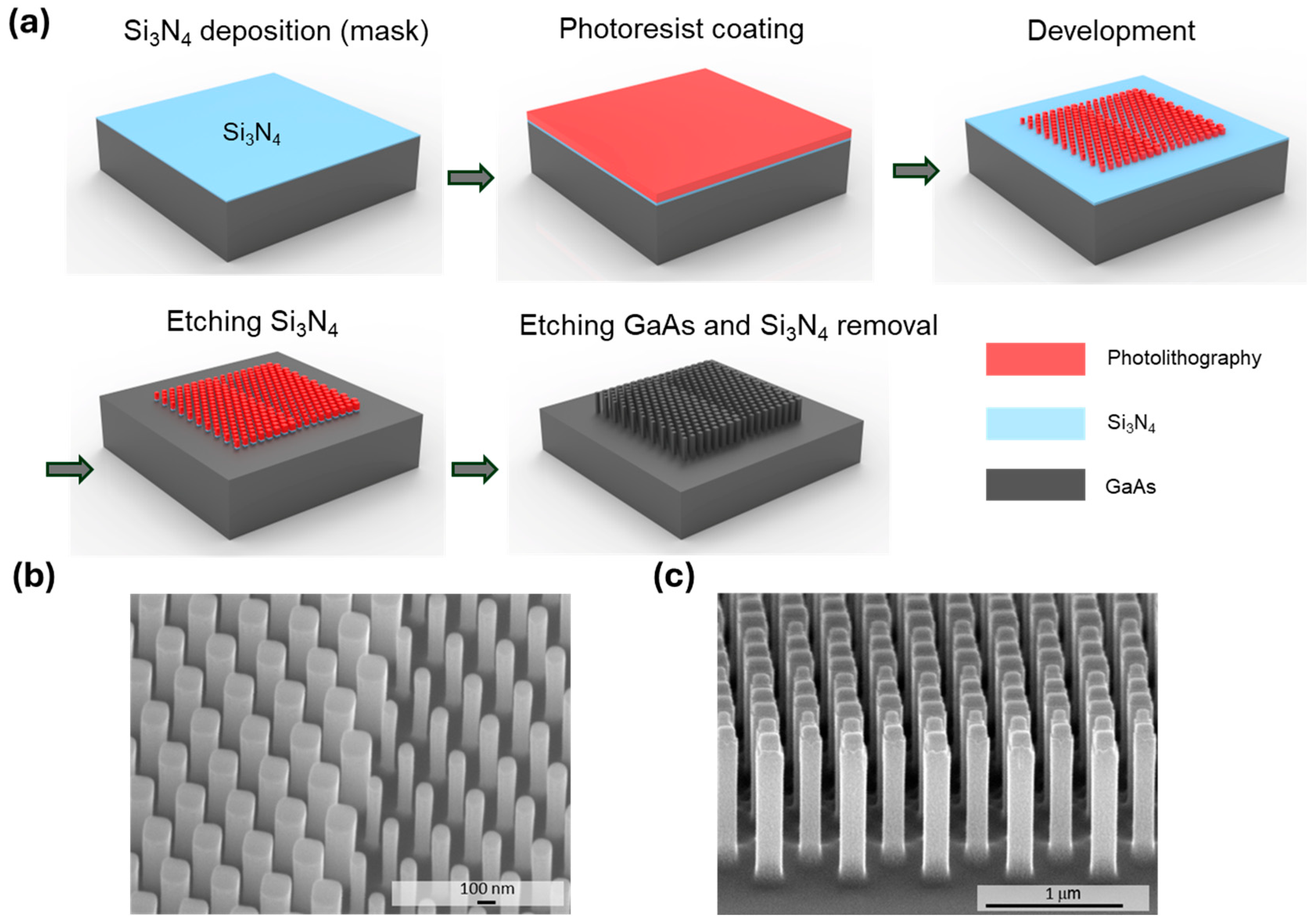
3.1. Fabrication Process of Si Metagratings Operating at a Wavelength of 1550 nm

Following the simulation methods outlined in Section 2, we fabricated four different Si metagratings with varying diffraction angles using a top-down approach. The diffraction angles for these Si metagratings ranged from 19.0° to 60.3°.
The fabrication process for Si metagrating is depicted in Figure 3a. Initially, a 100 nm thick layer of SiO2 was deposited on a 725 µm thick Si substrate using plasma-enhanced chemical vapor deposition (PECVD, 100PECVD cassette system, Oxford Instrument). This served as a hard mask for subsequent Si etching. A negative electron beam resist (ma-N 2403, Micro Resist Technology) was then applied using a spin coater. An electron beam lithography system (VOYAGER, Raith) was then utilized to define metagrating patterns within a 500 µm × 500 µm area. The SiO2 layer was then etched using reactive ion etching (Lam2300, Lam Research) to transfer the metagrating pattern from the negative electron beam resist to the hard mask layer. Acetone was subsequently used to remove any remaining electron beam resist. The Si substrate was then etched using a plasma enriched with HBr and Cl2 precursors. Finally, the SiO2 layer was removed using buffered oxide etchant (BOE), and Cr apertures, 300 nm thick, were created using a lift-off process with a double-sided mask aligner (AG1000, M&R Nano Technology) and a high-vacuum thermal evaporator (TH-400, Lj-Uhv Technology). The Cr apertures were created to confine the region of interaction between the light and the metagrating, thereby measuring the efficiency.
We employed scanning electron microscopy (SEM, SU8010, Hitachi) to obtain images of Si metagrating. The side view presented in Figure 3b reveals an image containing a Si supercell, demonstrating that the unit cells were successfully etched to form nanostructures. Figure 3c presents a SEM side view of a Si metagrating. It depicts a Si nanopillar with a height of approximately 931 nm. This height aligns with our design specifications for Si metagratings.

3.2. Fabrication Process of GaAs Metagratings Operating at a Wavelength of 940 nm

Based on our previous design and simulation of a GaAs-based metasurface operating at 940 nm capable of integration with GaAs-based VCSELs and PCSELs [24], we also produced four different homo-metagratings with varying diffraction angles using a top-down approach. The designed diffraction angles ranged from 19.7° to 49.3°.
Figure 4a illustrates the fabrication process of the GaAs samples. Initially, we deposited a 100 nm thick Si3N4 layer using plasma-enhanced chemical vapor deposition (PECVD) with a Plasmalab80Plus (Oxford Instrument) as a hard mask for etching GaAs. Next, to prepare for lithography, a negative electron beam resist (ma-N 2403, Micro Resist Technology) was applied using a spin coater. We then defined the metagrating patterns over an area of 500 µm × 500 µm using electron beam lithography (VOYAGER, Raith). Following this, the Si3N4 layer was etched using inductively coupled plasma (Plasmalab System 100, Oxford Instrument), after which the resist was removed with acetone. Subsequently, by utilizing Ar and SiCl4 as precursors in a plasma etching process, GaAs nanopillars were formed. Finally, we used buffered oxide etchant (BOE) to remove any residual unetched Si3N4 layer. To standardize the measurement of the diffraction efficiency, we fabricated apertures measuring 500 µm × 500 µm. This ensured that the power of incident light remained constant across each metagrating. To this end, we applied a layer of photoresist (AZ-P4620, AZ Electronic Materials) using a spin coater. Subsequently, the positive photoresist was exposed using a double-sided mask aligner (AG1000, M&R Nano Technology). Finally, a 300 nm thick layer of Cr was deposited using a high-vacuum thermal evaporator (TH-400, Lj-Uhv Technology). This was followed by a lift-off process to fabricate the apertures. The Cr apertures were deposited for the efficiency measurement.
We captured images of one GaAs metagrating using a scanning electron microscope (SEM, S-4700I, Hitachi), as shown in Figure 4b,c. Figure 4c shows that the height of the GaAs nanopillars was about 857 nm, which conformed to our design specifications for GaAs metagrating. The narrower tops of the nanopillars are due to the more severe lateral etching of GaAs at the beginning of the etching process.

4. Efficiency Measurements

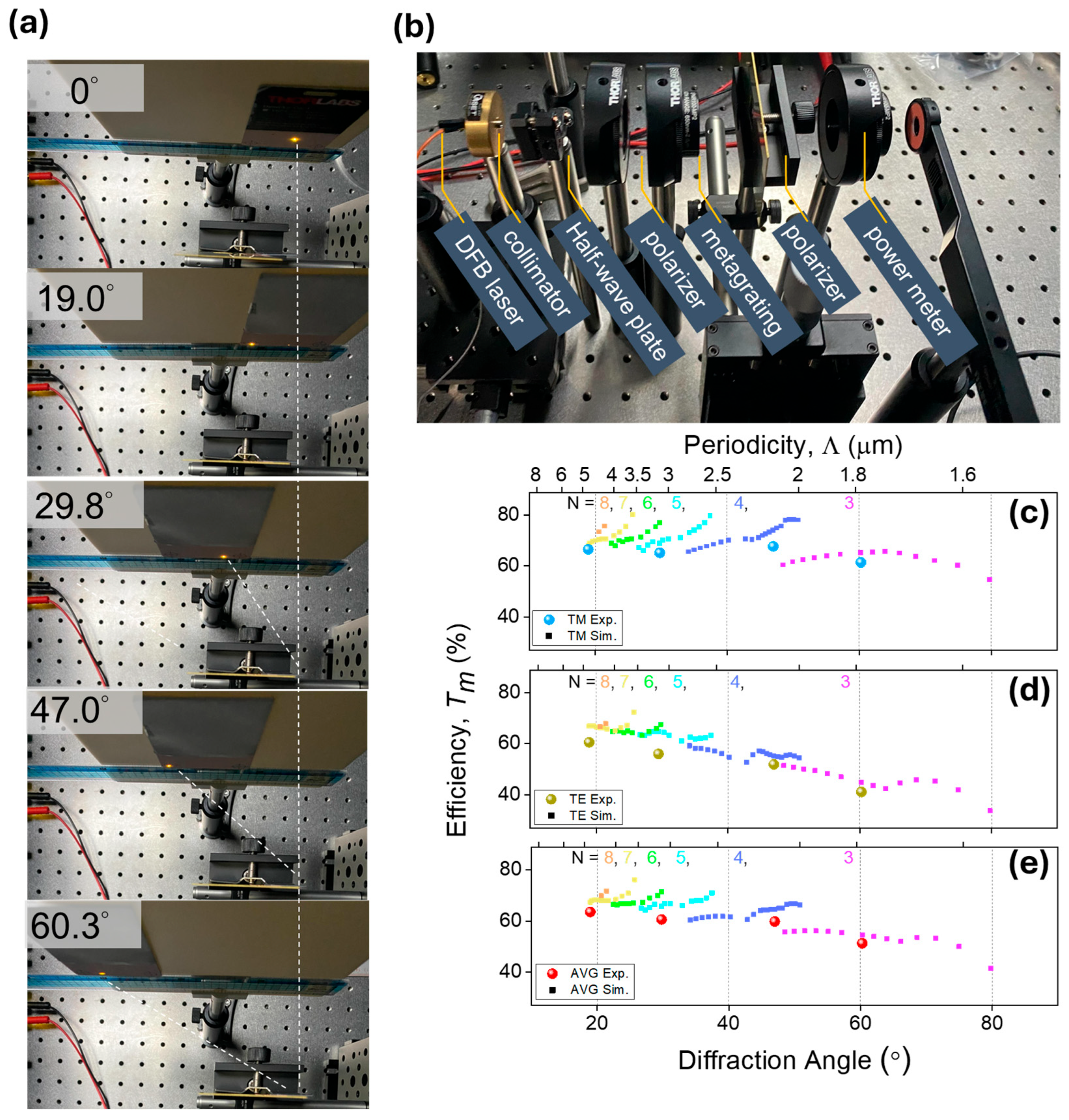
4.1. Measurement Setup and Results for Si Metagrating

The Si metagratings are capable of integration with VCSELs and DFB lasers as the light source for a 1550 nm wavelength. Due to the facilitation of efficiency measurements by a higher laser power and the absence of commercial PCSELs for a 1550 nm wavelength, we opted to use DFB lasers as our measurement light source. Compared to commercial PCSELs, DFB lasers have a larger divergence angle, necessitating the addition of a collimator between the laser and metasurfaces to collimate the light beam for subsequent measurements. The current injected into the DFB laser was 300 mA. Figure 5a shows a photograph captured from a 0° angle, illustrating the path of a light beam. This beam traversed a collimator (LTN330-C, Thorlabs), the Si substrate, and a metal aperture located on the substrate. It was then projected onto a far-field screen situated z = 10 cm away. Following this, the laser light was steered onto various Si metagratings by adjusting a three-axis stage. As shown in Figure 5b, rotating a half-wave plate (WPH10E-1550, Thorlabs) allowed the laser light to impinge on the metagratings with maximum power, while two linear polarizers (LP) were placed to ensure the polarization state of the light beam. The measurements and simulation data for the Si metagratings, which were 900 nm in height and arranged in a hexagonal lattice, are shown in Figure 5c–e. Compared to the lattice constants of GaAs metagratings ranging from 300 nm to 400 nm, we simulated a larger lattice range from 500 nm to 690 nm with a more extensive set of unit cell numbers (N) from three to eight to optimize the diffraction efficiency of Si metagratings with diffraction angles ranging from 19.0° to 79.7°. The efficiency most commonly examined in measurement is either the absolute efficiency or the relative efficiency. Considering the differences between the simulated efficiency and measured efficiency, we utilized the diffraction efficiency (Tm) for the comparison of efficiencies. The conversion between measured and simulated diffraction efficiencies is explained in our previous article [24]. In Figure 5c, the cyan dots represent the TM polarization diffraction efficiency measured through the optical setup shown in Figure 5b. The dark amber dots in Figure 5d represent the TE polarization measurement efficiency. Finally, Figure 5e shows the average of the TM and TE polarizations, with red dots indicating the average values measured at the same diffraction angle. At a diffraction angle of 60.3°, the Si metasurfaces still exhibited a diffraction efficiency of 51.3%.
From Figure 5c–e, it can be observed that the simulation data represent the intrinsic diffraction efficiency of the metasurface itself. In the experiments, the measured diffraction efficiency, when multiplied by 1.44 (representing the impedance matching from air to the metasurface substrate), matches the previously mentioned diffraction efficiency (Tm) of the metasurface. When simulating metagratings, the simulated incident light originates from the substrate material. However, in actual measurements, the laser light first passes through the air before reaching the substrate. Therefore, if we only measure the power of the laser incident on the air as the total power reference, this does not align with the conditions of the incident light in our simulations. To maintain consistency with the conditions used in our metagrating simulations, we adjusted the measured diffracted light power by multiplying it by 1.44 to meet the simulation conditions.
To account for laser power reduction due to refractive index mismatch on a substrate, the transmittance Tij of laser light from air to a silicon substrate at 1550 nm, where the refractive index of air is 1.00 and that of silicon is 3.48, is calculated as follows:
T i j = 4 n i n j ( n i + n j ) 2
The transmittance of the light is T12 = 69.4%. Taking the reciprocal of 69.4% yields 1.44. The refractive index of GaAs at a working wavelength of 940 nm is 3.51. The transmittance of light (T12) from air to the substrate, after the laser passes through the substrate, is 69.1%. Therefore, when measuring the power of the laser light incident from air to the superlattice interface, it also needs to be multiplied by 1.44 to compensate for the impedance matching between air and the GaAs substrate.
In the design of the metagrating, the diffraction angles were adjusted by modifying the lattice constant (U) and the number of unit cells (N) in the metagrating. Subsequently, the DOF of the phase was utilized to optimize the diffraction efficiency at these angles. When the metagrating was specifically designed for a certain diffraction angle, a noticeable discrepancy between the measured and simulated diffraction efficiencies was observed. The lower measured efficiency compared to the simulated efficiency is likely caused by slight inaccuracies in the height of our Si metagrating samples.

4.2. Measurement Setup and Results for GaAs Metagrating

In the practical measurements, a commercial PCSEL (L13395-04, Hamamatsu) was used as the light source for a 940 nm wavelength. Figure 6a depicts a scenario where, initially, a beam from the PCSEL passes through a GaAs substrate and the apertures on it. The current injected into the PCSEL was 300 mA. The beam was projected onto a far-field screen located at a distance of z = 10 cm. Subsequently, by directing the PCSEL onto different GaAs samples using a three-axis stage, we achieved varying diffraction angles. GaAs metagratings were designed for diffraction at 19.7°, 30.4°, 37.3°, and 49.3°. The polarization state of both the incident and diffracted light was controlled by adjusting two linear polarizers (LP, LPNIR100-MP2, Thorlabs). One polarizer was placed between the light source and the GaAs metagratings, tasked with generating either TE or TM polarized light. The other polarizer functioned as an analyzer, specifically designed to assess the polarization state of the diffracted light. The diffraction efficiency was measured based on the power recorded by a power meter (PM100D, S120C, Thorlabs) after the laser passed through the polarizer, the GaAs substrate, and the apertures, as shown in Figure 6b.
Measurements and simulation data for the metagratings with a height of 800 nm are presented in Figure 6c–e. The simulated data points were already presented in our previous article. The simulated data in Figure 6c indicate that it is possible to select a metagrating with a higher diffraction efficiency for fabrication when the diffraction angles are similar (gray area). Moreover, the metagratings achieved a higher diffraction efficiency when the lattice constant was 310 nm. This is attributed to the increase in the average transmittance through the unit cell and the expansion of the phase optimization range. In the experiments, the measured diffraction efficiency, when multiplied by 1.44 (representing the impedance matching from the air to the GaAs metasurface substrate), equated to the diffraction efficiency of the metasurface (Tm). In Figure 6c, the blue dots represent the overall diffraction efficiency for TM polarization of our simulated metagratings arranged in a hexagonal lattice. The cyan dots represent the overall efficiency for TM polarization measured for the light after passing through two linear polarizers and the metasurfaces, with refractive index matching from the air to the substrate considered. In Figure 6d, the amber dots represent the simulated overall diffraction efficiency for TE polarization, while the dark amber dots are the efficiencies measured through experiments. We simulated a metagrating with a square lattice arrangement, and the highest average diffraction efficiency is presented in Figure 6e. The red dots represent the overall average efficiency measured. At a diffraction angle of approximately 30° for the metagrating, we measured an average overall diffraction efficiency of 70.3%, which is about 1.6 times higher than the efficiency reported in the literature [23]. It was observed that the larger the diffraction angle, the greater the deviation of the actual efficiency from our simulations. As the diffraction angle decreases, so does the order of the phase. This means that distortion in a single unit cell can reduce the metasurface’s ability to manipulate light. Additionally, distortions in the top patterns of our nanopillars and slight inaccuracies in the height of our metagrating samples led to a decrease in the measured diffraction efficiency.

5. Discussion and Conclusions

We assessed the disparities between the simulated and actual measured efficiencies of homogeneous metasurface gratings made from GaAs and Si. The data in Figure 5e indicate that the actual measured efficiency of the Si metagratings closely aligns with the simulated diffraction efficiency. However, Figure 6e reveals a significant divergence between the simulated and actual measured efficiencies for GaAs. This discrepancy primarily stems from slight etching on the sidewalls at the top of the GaAs nanopillars, as illustrated in Figure 4c. Such structural variations cause deviations from the original design of the actual nanopillars, consequently diminishing the measured efficiency.
In summary, we focused on the simulation of high-efficiency Si metagratings, with an emphasis on maximizing the overall efficiency while ensuring eye safety. By maintaining the degree of freedom for the phase (δ), the number of unit cells (N), and the lattice constant (U) of the unit cell, we were able to optimize the metagrating to enhance performance. Furthermore, we fabricated metagratings using Si and GaAs, validating the effectiveness of our design approach.
Specifically, the Si metagrating demonstrated an overall diffraction efficiency of 51.3% at a diffraction angle of 60.3°. Similarly, the GaAs metagrating we developed achieved an impressive overall average efficiency of 65.5% at a diffraction angle of 30°. This performance is 1.6 times higher than that reported in the literature, marking a significant advancement in the field [23]. This also showcases the potential of our design method.
Our selection process for the metagratings focused on those with the highest average efficiency. However, should we opt to specifically choose patterns demonstrating the highest efficiency for TM and TE polarizations, it stands to reason that we could achieve a further enhancement in efficiency.
It is important to note that both types of metagrating, designed with a propagation phase, exhibited a higher diffraction efficiency of TM polarization. This finding suggests that further improvements in the overall efficiency can be achieved by controlling the polarization direction of light. Such technological advancements are anticipated to enhance the energy efficiency and extend the transmission distance of light sources, offering substantial potential for applications in LiDAR [28,29], VR [30,31], and depth sensing [14]. This research not only paves the way for the development of more efficient and safer optical devices but also opens new avenues for innovation in photonic technologies.

Author Contributions

Y.-W.H. initiated the study. W.-C.T. and Y.-H.H. (Yi-Hsuan Huang) performed the numerical calculation and simulation. W.-C.T. and C.-H.C. fabricated samples. W.-C.T. and Y.-H.H. (Yi-Hsuan Huang) performed the optical experiments. H.-C.K., Y.-W.H., and C.-W.C. contributed the required materials and analysis tools. W.-C.T. and Y.-W.H. analyzed the experimental data. W.-C.T., Y.-H.H. (Yu-Heng Hong), H.-C.K., and T.-C.Y. discussed the simulation and experimental results. W.-C.T. and Y.-W.H. wrote the manuscript. All authors commented on the manuscript. All authors have read and agreed to the published version of the manuscript.

Funding

National Science and Technology Council, Taiwan (Grant Nos. 110-2622-8-A49-008-SB, 111-2622-8-A49-021-SB, 112-2622-8-A49-020, and 110-2112-M-A49-034-MY3).

Institutional Review Board Statement

Not applicable.

Informed Consent Statement

Not applicable.

Data Availability Statement

The data presented in this study are available upon reasonable request from the corresponding authors.

Acknowledgments

The authors acknowledge support from the National Science and Technology Council (NSTC) in Taiwan and the Ministry of Education in Taiwan under the Yushan Young Scholar Program and the Higher Education Sprout Project of the National Yang Ming Chiao Tung University. We also acknowledge the Semiconductor Research Center, Foxconn Research, for their technical support. This work was performed in part at the Nano Facility Center (NFC) at NYCU, the Center for Nano Science and Technology (CNST) at NYCU, and the Taiwan Semiconductor Research Institute (TSRI).

Conflicts of Interest

The authors declare no conflicts of interest.

References

  1. Hong, Y.-H.; Hsu, W.-C.; Tsai, W.-C.; Huang, Y.-W.; Chen, S.-C.; Kuo, H.-C. Ultracompact Nanophotonics: Light Emission and Manipulation with Metasurfaces. Nanoscale Res. Lett. 2022, 17, 41. [Google Scholar] [CrossRef]
  2. Hsiao, H.-H.; Chu, C.H.; Tsai, D.P. Fundamentals and Applications of Metasurfaces. Small Methods 2017, 1, 1600064. [Google Scholar] [CrossRef]
  3. Yu, N.; Capasso, F. Flat Optics with Designer Metasurfaces. Nat. Mater. 2014, 13, 139–150. [Google Scholar] [CrossRef]
  4. Tseng, M.L.; Hsiao, H.-H.; Chu, C.H.; Chen, M.K.; Sun, G.; Liu, A.-Q.; Tsai, D.P. Metalenses: Advances and Applications. Adv. Opt. Mater. 2018, 6, 1800554. [Google Scholar] [CrossRef]
  5. Lin, D.; Fan, P.; Hasman, E.; Brongersma, M. Dielectric Gradient Metasurface Optical Elements. Science 2014, 345, 298–302. [Google Scholar] [CrossRef]
  6. Chen, W.T.; Zhu, A.Y.; Sanjeev, V.; Khorasaninejad, M.; Shi, Z.; Lee, E.; Capasso, F. A Broadband Achromatic Metalens for Focusing and Imaging in the Visible. Nat. Nanotechnol. 2018, 13, 220–226. [Google Scholar] [CrossRef]
  7. Wang, S.; Wu, P.C.; Su, V.-C.; Lai, Y.-C.; Chen, M.-K.; Kuo, H.Y.; Chen, B.H.; Chen, Y.H.; Huang, T.-T.; Wang, J.-H.; et al. A Broadband Achromatic Metalens in the Visible. Nat. Nanotechnol. 2018, 13, 227–232. [Google Scholar] [CrossRef]
  8. Li, X.; Chen, C.; Guo, Y.; He, Q.; Zhang, R.; Pu, M.; Chen, X.; Jin, X.; Li, H.; Luo, X. Monolithic Spiral Metalens for Ultrahigh-Capacity and Single-Shot Sorting of Full Angular Momentum State. Adv. Funct. Mater. 2024, 34, 2311286. [Google Scholar] [CrossRef]
  9. Wen, D.; Meng, J.; Cadusch, J.J.; Crozier, K.B. VCSELs with On-Facet Metasurfaces for Polarization State Generation and Detection. Adv. Opt. Mater. 2021, 9, 2001780. [Google Scholar] [CrossRef]
  10. Huang, Y.; Xiao, T.; Chen, S.; Xie, Z.; Zheng, J.; Zhu, J.; Su, Y.; Chen, W.; Liu, K.; Tang, M.; et al. All-Optical Controlled-NOT Logic Gate Achieving Directional Asymmetric Transmission Based on Metasurface Doublet. OEA 2023, 6, 220073–220079. [Google Scholar] [CrossRef]
  11. Tang, Z.; Li, L.; Zhang, H.; Yang, J.; Hu, J.; Lu, X.; Hu, Y.; Qi, S.; Liu, K.; Tian, M.; et al. Multifunctional Janus Metasurfaces Achieving Arbitrary Wavefront Manipulation at Dual Frequency. Mater. Des. 2022, 223, 111264. [Google Scholar] [CrossRef]
  12. Zheng, G.; Mühlenbernd, H.; Kenney, M.; Li, G.; Zentgraf, T.; Zhang, S. Metasurface Holograms Reaching 80% Efficiency. Nat. Nanotechnol. 2015, 10, 308–312. [Google Scholar] [CrossRef]
  13. Lin, C.-H.; Huang, S.-H.; Lin, T.-H.; Wu, P.C. Metasurface-Empowered Snapshot Hyperspectral Imaging with Convex/Deep (CODE) Small-Data Learning Theory. Nat. Commun. 2023, 14, 6979. [Google Scholar] [CrossRef]
  14. Hsu, W.-C.; Chang, C.-H.; Hong, Y.-H.; Kuo, H.-C.; Huang, Y.-W. Metasurface- and PCSEL-Based Structured Light for Monocular Depth Perception and Facial Recognition. Nano Lett. 2024, 24, 1808–1815. [Google Scholar] [CrossRef]
  15. Wu, P.C.; Tsai, W.-Y.; Chen, W.T.; Huang, Y.-W.; Chen, T.-Y.; Chen, J.-W.; Liao, C.Y.; Chu, C.H.; Sun, G.; Tsai, D.P. Versatile Polarization Generation with an Aluminum Plasmonic Metasurface. Nano Lett. 2017, 17, 445–452. [Google Scholar] [CrossRef]
  16. Zhang, F.; Pu, M.; Li, X.; Ma, X.; Guo, Y.; Gao, P.; Yu, H.; Gu, M.; Luo, X. Extreme-Angle Silicon Infrared Optics Enabled by Streamlined Surfaces. Adv. Mater. 2021, 33, 2008157. [Google Scholar] [CrossRef]
  17. Shi, T.; Wang, Y.; Deng, Z.-L.; Ye, X.; Dai, Z.; Cao, Y.; Guan, B.-O.; Xiao, S.; Li, X. All-Dielectric Kissing-Dimer Metagratings for Asymmetric High Diffraction. Adv. Opt. Mater. 2019, 7, 1901389. [Google Scholar] [CrossRef]
  18. Zhou, Z.; Li, J.; Su, R.; Yao, B.; Fang, H.; Li, K.; Zhou, L.; Liu, J.; Stellinga, D.; Reardon, C.P.; et al. Efficient Silicon Metasurfaces for Visible Light. ACS Photonics 2017, 4, 544–551. [Google Scholar] [CrossRef]
  19. Sell, D.; Yang, J.; Doshay, S.; Yang, R.; Fan, J.A. Large-Angle, Multifunctional Metagratings Based on Freeform Multimode Geometries. Nano Lett. 2017, 17, 3752–3757. [Google Scholar] [CrossRef]
  20. Ni, P.-N.; Fu, P.; Chen, P.-P.; Xu, C.; Xie, Y.-Y.; Genevet, P. Spin-Decoupling of Vertical Cavity Surface-Emitting Lasers with Complete Phase Modulation Using on-Chip Integrated Jones Matrix Metasurfaces. Nat. Commun. 2022, 13, 7795. [Google Scholar] [CrossRef]
  21. Fu, P.; Ni, P.-N.; Wu, B.; Pei, X.-Z.; Wang, Q.-H.; Chen, P.-P.; Xu, C.; Kan, Q.; Chu, W.-G.; Xie, Y.-Y. Metasurface Enabled On-Chip Generation and Manipulation of Vector Beams from Vertical Cavity Surface-Emitting Lasers. Adv. Mater. 2023, 35, 2204286. [Google Scholar] [CrossRef]
  22. Xie, Y.-Y.; Ni, P.-N.; Wang, Q.-H.; Kan, Q.; Briere, G.; Chen, P.-P.; Zhao, Z.-Z.; Delga, A.; Ren, H.-R.; Chen, H.-D.; et al. Metasurface-Integrated Vertical Cavity Surface-Emitting Lasers for Programmable Directional Lasing Emissions. Nat. Nanotechnol. 2020, 15, 125–130. [Google Scholar] [CrossRef]
  23. Wang, Q.-H.; Ni, P.-N.; Xie, Y.-Y.; Kan, Q.; Chen, P.-P.; Fu, P.; Deng, J.; Jin, T.-L.; Chen, H.-D.; Lee, H.W.H.; et al. On-Chip Generation of Structured Light Based on Metasurface Optoelectronic Integration. Laser Photonics Rev. 2021, 15, 2000385. [Google Scholar] [CrossRef]
  24. Tsai, W.-C.; Hong, Y.-H.; Kuo, H.-C.; Huang, Y.-W. Design of High-Efficiency and Large-Angle Homo-Metagratings for Light Source Integration. Opt. Express OE 2023, 31, 24404–24411. [Google Scholar] [CrossRef]
  25. Angelini, F.; Colao, F. Optimization of Laser Wavelength, Power and Pulse Duration for Eye-Safe Raman Spectroscopy. J. Eur. Opt. Soc. Rapid Publ. 2019, 15, 2. [Google Scholar] [CrossRef]
  26. Cheng, J.-X. New “HOPE” Laser for Photoacoustic Imaging of Water. Light. Sci. Appl. 2022, 11, 107. [Google Scholar] [CrossRef]
  27. Hugonin, J.P.; Lalanne, P. RETICOLO Software for Grating Analysis. arXiv 2023, arXiv:2101.00901v3. [Google Scholar]
  28. Kim, I.; Martins, R.J.; Jang, J.; Badloe, T.; Khadir, S.; Jung, H.-Y.; Kim, H.; Kim, J.; Genevet, P.; Rho, J. Nanophotonics for Light Detection and Ranging Technology. Nat. Nanotechnol. 2021, 16, 508–524. [Google Scholar] [CrossRef]
  29. Wang, D.; Watkins, C.; Xie, H. MEMS Mirrors for LiDAR: A Review. Micromachines 2020, 11, 456. [Google Scholar] [CrossRef]
  30. Li, Z.; Lin, P.; Huang, Y.-W.; Park, J.-S.; Chen, W.T.; Shi, Z.; Qiu, C.-W.; Cheng, J.-X.; Capasso, F. Meta-Optics Achieves RGB-Achromatic Focusing for Virtual Reality. Sci. Adv. 2021, 7, eabe4458. [Google Scholar] [CrossRef]
  31. Li, Z.; Pestourie, R.; Park, J.-S.; Huang, Y.-W.; Johnson, S.G.; Capasso, F. Inverse Design Enables Large-Scale High-Performance Meta-Optics Reshaping Virtual Reality. Nat. Commun. 2022, 13, 2409. [Google Scholar] [CrossRef]
Figure 1. (a) The schematic shows the measurement setup using metasurfaces and a laser to measure diffraction efficiency. (b) The schematic illustrates the definition of polarization relative to the diffraction plane (y–z plane).
Photonics 11 00392 g001
Figure 2. (a) Calculated transmission and phase coverage for square Si nanopillars as a function of their width, operating at a wavelength of 1550 nm. The inset represents a nanopillar in hexagonal arrangement. (b) Simulated diffraction efficiency (for TM mode, TE mode, and their average) at a deflection angle of 60.3° versus different DOFs of the overall add-on phase. (c) Diffraction efficiency range of Si metagratings in TM mode, TE mode, and average mode with a diffraction angle of 60.26°.
Photonics 11 00392 g002
Figure 3. (a) Fabrication flow of Si metagratings. (b) Side-view SEM image of fabricated Si-based metagratings. (c) Close-up SEM image of the sample.
Photonics 11 00392 g003
Figure 4. (a) Fabrication process of GaAs metagratings. (b) Side-view SEM images of GaAs fabricated metagratings. (c) Close-up SEM image of the sample.
Photonics 11 00392 g004
Figure 5. Experiment results for the Si metagratings. (a) Measured beam spots projected onto a far-field screen at z = 10 cm from the metasurface samples. The diffraction angles of the samples demonstrate their design in the range from 19.0° to 60.3°. (b) Side-view photography of the optical setup. Overall efficiency results of the simulations and measurements in (c) TM mode and (d) TE mode, and (e) the average efficiency for Si metasurfaces.
Photonics 11 00392 g005
Figure 6. Experiment results for the GaAs metagratings. (a) Measured beam spots projected onto a far-field screen at z = 10 cm from metasurface samples. The diffraction angles of the samples demonstrate their design in the range from 19.7° to 49.3°. (b) Side-view photography of the optical setup. Overall efficiency results of the simulations and measurements in (c) TM mode and (d) TE mode and (e) the average efficiency for GaAs metasurfaces.
Photonics 11 00392 g006
Disclaimer/Publisher’s Note: The statements, opinions and data contained in all publications are solely those of the individual author(s) and contributor(s) and not of MDPI and/or the editor(s). MDPI and/or the editor(s) disclaim responsibility for any injury to people or property resulting from any ideas, methods, instructions or products referred to in the content.

