1. Introduction
Common optical refractive index sensors include optical fiber optic sensors [
1], micro-ring resonator sensors [
2], photonic crystal sensors [
3], and surface plasmon resonance (SPR) sensors. Photonic devices excel over electronic devices in operating bandwidth; however, their miniaturization and integration are constrained by the optical diffraction limit, which in turn limits the development of optical refractive index sensor sizes [
4]. However, surface plasmon polaritons (SPPs) are capable of exceeding the diffraction limit and can precisely manipulate light on the nanoscale [
5]. Consequently, an increasing number of scholars are focusing on SPPs.
Surface plasmon polaritons (SPPs) are electromagnetic waves are formed by the intricate interplay between the free electrons of the metal and incident photons [
6], enabling the over-coming of diffraction limits and allowing for the precise manipulation of light at the nanoscale [
7]. Therefore, SPPs have immense promise for applications in integrated optical circuits and subwavelength photonic devices, ushering in a new era of transformative possibilities in nanophotonics. This electromagnetic wave can propagate across the interfaces and confine the field energy to a small region around the interfaces, resulting in a rapid decrease in intensity in the direction perpendicular to the interfaces [
8]. SPP (surface plasmon polariton) waveguides provide significant advantages in photonics, chiefly through their ability to overcome the physical limitations of the diffraction limit that constrain conventional dielectric waveguides. This property enables the control and manipulation of light at sub-wavelength dimensions, thus facilitating the development of ultra-compact and highly efficient photonic devices. Due to their unmatched nanoscale light manipulation capabilities, SPPs are at the forefront of next-generation photonic technology, serving as the cornerstone for developing highly integrated chip-scale photonic devices. In addition, the potential for the seamless integration of SPPs with existing semiconductor platforms heralds new possibilities for advancements in optical computing and communications, positioning them as key innovations in optoelectronics and nanotechnology [
9,
10].
Surface plasmon excitations markedly enhance the electromagnetic field at the metal–dielectric interface, a phenomenon of critical importance for optical sensing and information processing. Firstly, the composite structure of micro- and nanomaterials reacts to these excitations through optical nonlinear effects, rendering the system highly sensitive to the local structure of the metal surface and to refractive index changes in the medium. This sensitivity not only aids in detecting changes in the surface morphology and refractive index but also enables the fabrication of devices such as surface plasmon resonance sensors [
11,
12,
13], all-optical switches [
14], and optical modulators [
15]. These devices find widespread use in various fields, including biomolecular detection, chemical analysis, environmental monitoring, and optical communication, offering key technologies for optical sensing, super-resolution imaging, and information processing and transmission. These functions are crucial in the fields of nanophotonics, optical sensing, photonic chips, and surface-enhanced spectroscopy and serve as the foundation for developing novel nanophotonic devices, underscoring their significant application value in modern optoelectronics [
16].
Surface plasmon polaritons (SPPs) can not only be generated at metal–dielectric interfaces but can also be excited through various waveguide structures, including metal– dielectric–metal (MIM) [
17], dielectric–metal–dielectric [
18], and dielectric–dielectric–metal [
19] waveguides. In particular, MIM waveguides have attracted attention due to their excellent SPP confinement, low ohmic losses, and long transmission distances [
20]. These waveguide systems can be designed with various structures to tune broadband and narrowband modes, achieving precise control of Fano resonances. Traditional MIM waveguide structures typically include straight waveguides and circular resonators to produce Fano resonances, but this method has certain performance limitations. Research has found that introducing defects into waveguides or resonators can effectively induce Fano resonances by disrupting propagation symmetry, enhancing performance. For example, by introducing a conical defect in a circular resonator, Rahmatiyar developed a new design for a nanoscale refractive index sensor, combining a ring resonator with an MIM waveguide [
21]. Further research explored plasmonic systems with defective silver nanoribbons, discovering that these systems can produce two Fano resonances. In these systems, quadrupole modes, which are not directly excitable on complete nanoribbons, become feasible through the introduction of defects. These defective silver nanoribbons support super radiant dipole and quadrupole modes, thereby producing two asymmetric Fano tilts in the transmission spectrum [
22]. Fei Hu’s work further demonstrated how adjusting the geometric parameters of silver nanorod defects, such as radius and the height or base length of an isosceles triangle resonator, can independently adjust the shape of the Fano resonances. These studies highlight the importance and potential of structural defects in designing nanophotonic devices with specific optical properties [
23].
Additionally, Yang and colleagues proposed a metal–insulator–metal (MIM) waveguide structure that includes a cross-shaped cavity and baffles. This structure achieved a sensitivity of 1075 nm/RIU [
24]. Wang and colleagues developed a structure that couples a metal–insulator–metal (MIM) waveguide with a semicircular cavity and two silver baffles, reaching a maximum sensitivity of 2200 nm/RIU [
25]. Pang and his team designed a novel structure using an MIM waveguide and an oblique rectangular cavity [
26]. Zhou presents a waveguide design incorporating two short stub resonators and a ring resonator. It achieves a peak sensitivity of 1650 nm/RIU and a figure of merit (FOM) of 117.8 [
27]. Tathfif reported a sensor composed of a straight waveguide, a groove, and a square ring resonator (SRR), with a maximum sensitivity of 1074.88 nm/RIU and a quality factor of 32.4 [
28]. Tang and colleagues proposed a sensor with a sensitivity of 1125 nm/RIU [
29]. Chen designed a structure with a semi-elliptical and rectangular ring resonator, achieving an optimal sensitivity of 1384 nm/RIU and a quality factor of 28.4 [
30]. This study proposes and investigates a new structure of a nanoscale refractive index sensor utilizing MIM waveguides, composed of an MIM bus waveguide and an internal Anchor-like resonator. It features relatively high sensitivity and quality factors, and the structure is simple, with a relatively small cavity area and low loss. Subsequently, we modified various structural parameters and the refractive index, observed changes in the transmission spectrum, and analyzed the impact on system sensing performance using the finite element method (FEM). Finally, it was applied in detecting hemoglobin concentrations in blood, and the sensor’s sensitivity was 0.6 nm·g/L, providing a theoretical basis for the field of nanomedicine.
2. Materials and Methods
This study utilized the finite element method to examine the relationship between the Fano resonance and changes in refractive index. We observed how the resonance frequency and intensity changed with the refractive index and analyzed the magnetic field distribution. By adjusting the structure’s geometrical parameters, including size and shape, we investigated their effects on Fano resonance. Given that the designed structure’s thickness is negligible compared to the spp surface depth, simulating the 3D structure requires more demanding hardware configuration and meshing. However, as the magnetic field characteristics of the 3D structure are largely similar to those of the 2D structure, we opted for the 2D model for simplicity in calculations [
31].
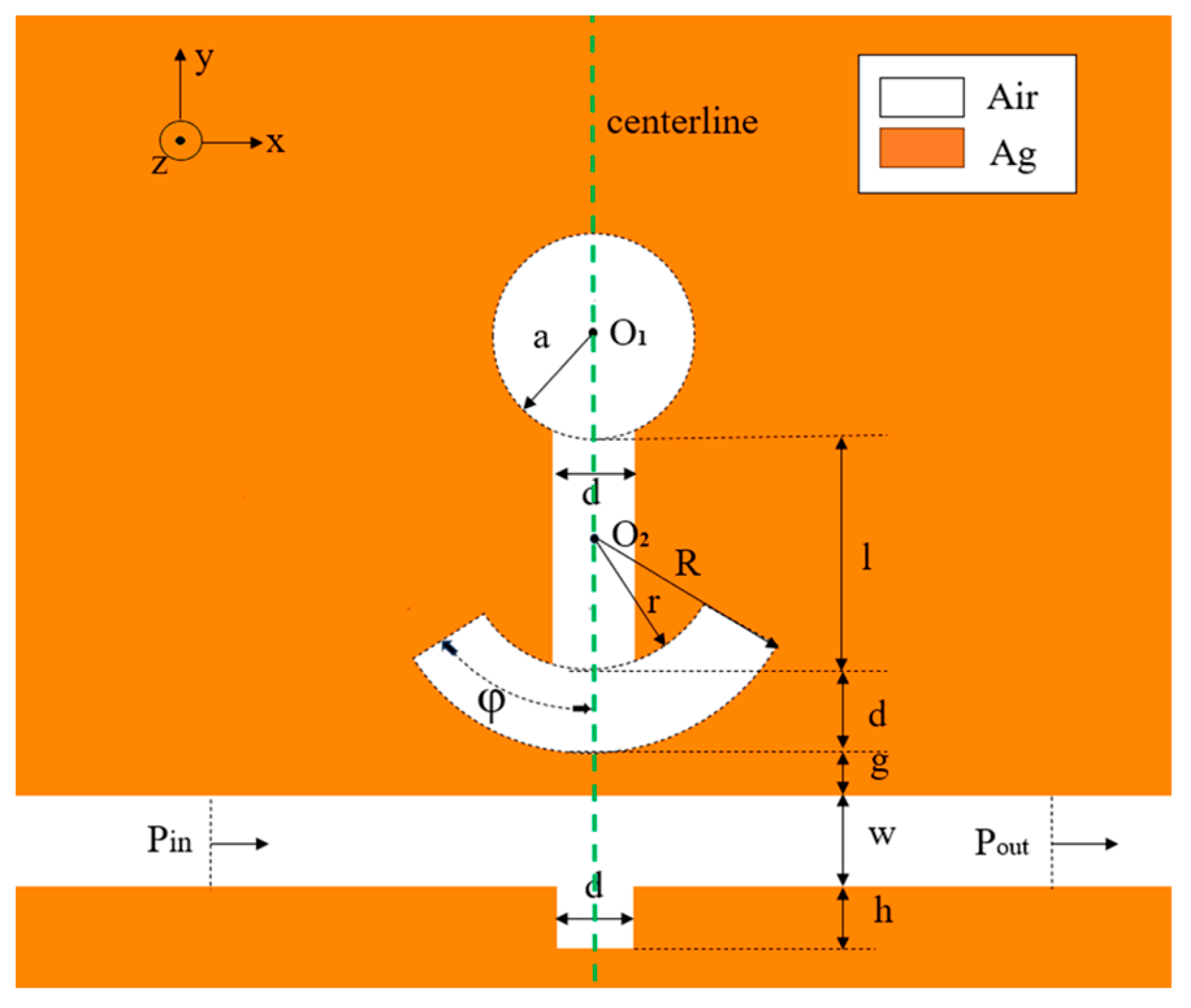
Figure 1 illustrates a 2D schematic of the symmetrical sensor structure along the centerline. As illustrated in
Figure 1, the system was modeled in COMSOL, with the Anchor-like structure comprising a circle, a rectangular waveguide, and a segment of a circular arc. Definitions are provided in the figure: a represents the radius of the upper circle, O
1 denotes the center of the upper circle, d is the width of the rectangular bar, r is the radius of the inner circle of the following arc, R represents the radius of the outer circle where R-r equals d, and the arc’s angle is 2φ. Here, g signifies the gap between the inverted rectangular waveguide and the Anchor-like, while w denotes the width of the waveguide. Additionally, l represents the distance between the lowest point of the upper circle and the lowest point of the inner circle of the arc, and the height of each individual rectangular bar is denoted by h.
Electromagnetic waves propagating along the metal–dielectric interface can be categorized into the two following basic modes according to the orientation of the electric and magnetic fields relative to the direction of propagation: transverse electric (TE) and transverse magnetic (TM) modes. In the TE mode, the electric field vector is completely transverse and perpendicular to both the direction of propagation and the metal–dielectric interface. Given that the electric field lacks a component parallel to the metal surface, it fails to effectively interact with the metal’s free electrons, thereby failing to excite surface plasmon polaritons (SPPs). Conversely, in the TM mode, the magnetic field vector is transverse to the direction of propagation, and the electric field includes a component along the interface. This electric field component can interact with the metal surface’s free electrons, inducing their collective oscillations and thereby exciting SPPs [
32,
33]. Therefore, our analysis concentrates on the TM mode, specifically investigating the relationship between surface plasmon polaritons (SPPs) and dispersion within this context [
34]:
where
k is the wave vector in the waveguide,
=
,
and
are the dielectric constants of the dielectric and the metal, respectively, and
p is the ratio of the permittivity
to the metal’s permittivity, and
is the free space wave vector.
A key design factor for metal–insulator–metal (MIM) waveguides involve the width of the dielectric layer (d). This dimension crucially affects the supported mode types and their levels of confinement. By matching the dielectric layer’s width with the waveguide’s (w), specifically at 50 nanometers, the design optimizes the transverse magnetic (TM) mode propagation conditions. It also aims to reduce or eliminate the transverse electric (TE) mode.
In
Figure 1, the yellow area represents silver, while the white part represents air. Silver was chosen as the filler metal for the following reasons: among all metallic elements, silver (Ag) has the smallest damping constant and is the best choice for performance at optical frequencies [
35], and silver is characterized by a high field strength and low system power; the properties of nanostructured silver make it the most suitable for next-generation plasmonic. We can prepare silver by achieving full deposition on the substrate using the chemical vapor deposition (CVD) and obtain the desired structure through electron beam etching [
36]. Considering that the dielectric constant of metallic materials varies with incident frequency, the dielectric constant of silver is modeled using the Drude–Debye approach (assuming a dielectric constant of 1 for air):
The parameter values are defined as follows: infinite frequency relative permittivity equals 3.8344, static dielectric strength is −9530.5, relaxation time is set at , conductivity σ amounts to , and represents the angular frequency of light at .
This study will evaluate the sensor’s performance using three parameters: FWHM, sensitivity (
S), and figure of merit (FOM). Sensitivity is crucial for assessing sensor performance. Fano resonance-based MIM waveguide structures detect changes in desired physical quantities by observing variations in wavelength position. In general, sensitivity is defined as follows [
37]:
Here, Δ
λ represents changes in refractive index, while Δ
n denotes changes in wavelength. Fano resonance manifests a distinctive feature in the transmission spectrum; the sharper the curve, the better the performance. We employ the full width at half maximum (FWHM) to characterize the spectrum’s sharpness, specifically, the width of the spectrum at half the height of the resonance peak, which is expressed as follows [
38]:
Here, Transmittance at
is (
Tmax +
Tmin)/2.
Tmax and
Tmin represent the maximum and minimum transmittance in the transmission spectrum. The figure of merit (FOM) is a crucial parameter for assessing sensors based on MIM waveguide structures and is defined as follows [
39]:
3. Simulation Results and Analysis
We employ COMSOL Multiphysics 5.4a software and a 2D modeling and analysis approach to investigate the frequency domain behavior of electromagnetic waves within the RF module. We focus on frequency domain analysis and boundary mode analysis as the subjects of our study. The 2D model is analyzed through simulation, and the geometric model of the designed sensor system is constructed. We establish the boundary absorption condition as a perfectly matched layer and utilize a free-profile triangular mesh along with hyper-refinement for mesh refinement in the waveguide and Anchor-like structure regions. Mesh refinement for other regions is performed using regularization. This strategy minimizes superfluous computations and upholds calculation precision. Initially, we begin by defining the various parameters of the sensor, the r = 140, R = 190, a = 75, d = h = w = 50 nm, l = 195 nm, g = 10 nm, and
φ = 60°.
Figure 2 displays the spectrograms of a single rectangular stub, all systems, and a single Anchor-like structure. These are represented by black, red, and blue curves, respectively. The wavelength range spans from 1700 nm to 2500 nm with 1 nm increments.
Spectral analysis reveals that the single anchor structure demonstrates low transmittance and a relatively symmetric shape, indicating a narrow-band mode directly excited by the incident light. Conversely, the transmission spectral profile of the single reverse waveguide structure displays a positive slope with high transmittance, implying a continuous broadband mode. Similarly, the transmission spectrum of a single rectangular stub, with its slightly upward-sloping curve and high transmittance for most optical signal frequencies, exhibits continuous broadband transmission characteristics, this phenomenon is classified as a continuous broadband mode. The structure reveals an asymmetric curve, signifying the clear presence of a Fano resonance. This phenomenon arises from the interaction between the continuous broadband states generated by the rectangular waveguide and the discrete narrowband states associated with each anchor-like structure, resulting in a significant Fano resonance. This phenomenon arises from the interaction between the anchor-like structures. Additionally, we investigated the effect of refractive index variation on the sensing performance of the designed structure.
Refractive indices ranging from n = 1.00 to n = 1.05 RIUs were simulated with constant structural parameters, as illustrated in
Figure 3a. With an increase in refractive index, the transmission spectrum exhibits an almost equidistant red shift. However, the change in refractive index does not alter the waveform of the transmission spectrum; it only shifts its position.
Figure 3b demonstrates a linear correlation between the wavelength and the refractive index, indicating the potential use of the proposed structure as a refractive index sensor. Through linear regression analysis to calculate the slope, the sensitivity of this sensor is determined to be 2440 nm/RIU, and the FOM is 63.
We discovered that the refractive index is only one factor influencing the Fano resonance, while the specific parameters of the structure can also significantly affect it as well. To delve deeper into the impact of these specific parameters, we initially adjusted the radius size, denoted as ‘a’, while keeping the center of circle
fixed. The radius range was set from 75 to 95 nm in steps of 5 nm, while all other structural parameters remained constant. The transmission spectra and sensitivity curves are illustrated in
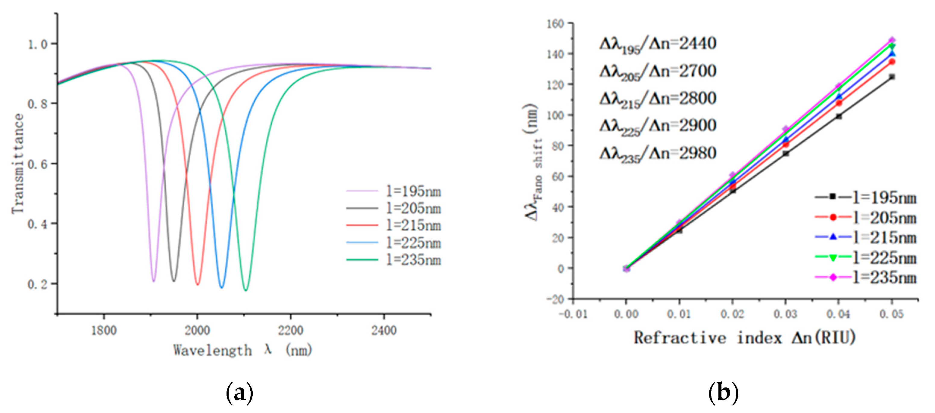
Figure 4. Subsequently, we explored the influence of another parameter, ‘l’, on the sensor’s propagation performance. Maintaining the distance between the lower arc and the waveguide constant, we shifted the upper circle relatively upward. The parameter ‘l’ varied from 195 nm to 235 nm with a step size of 10 nm, and the other parameters remained unchanged.
Figure 5 shows the simulation results.
The results above indicate a continuous redshift in the transmission spectrum as the radii a and l increase, accompanied by minor fluctuations in transmittance and FWHM. Additionally, we conducted linear fitting on resonance curves for various radii. As depicted in
Figure 4b, sensor sensitivity increases with larger radii a and l. Notably, the impact of a and l on sensor sensitivity is essentially identical. The maximum sensitivities are 2840 and 2980, respectively, for a = 95 and l = 195 nm.
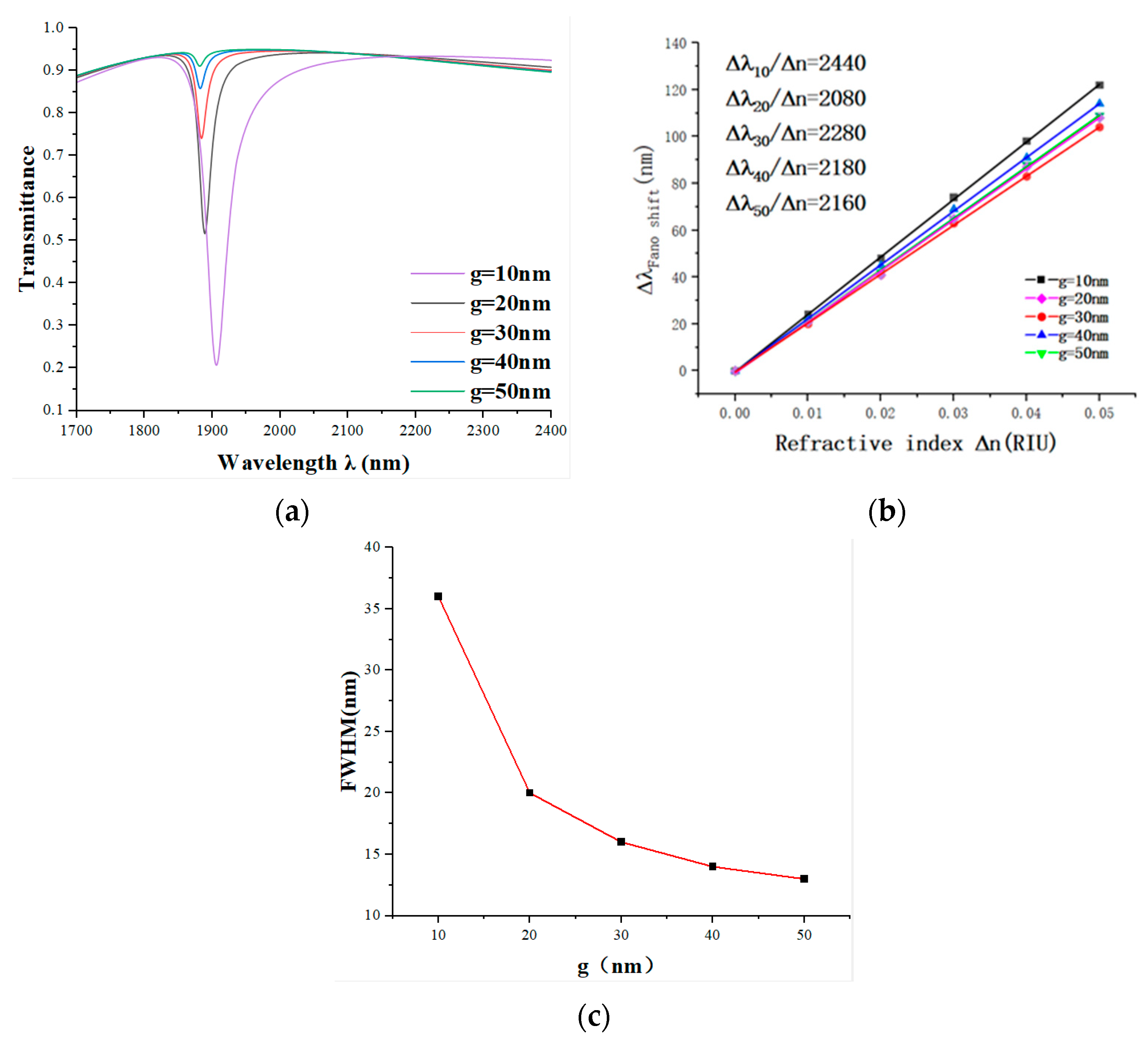
To delve deeper into the factors impacting sensor accuracy and to analyze the impact of the coupling gap on sensor performance, we vary the gap between the system and the anchor-like structure. We incrementally increased the coupling gap from 10 nm to 50 nm. As depicted in
Figure 6a, the curve noticeably blueshifts, and in
Figure 6c, we can see that FWHM significantly narrows with an increasing g. Additionally, Fano resonance curves are presented in
Figure 6a. The increasing transmittance of the Fano resonance curve indicates a notable deterioration in coupling performance, leading to a sharp decline in sensor performance. The sensitivity fitted line for various coupling gaps is illustrated in
Figure 6b. The most substantial sensitivity decrease occurs as g increases from 10 to 20. When g exceeds 10, the rate of change in sensor sensitivity decreases. However, when g is less than or equal to zero, implying direct contact between the two structures, the coupling effect becomes exceedingly strong, potentially inducing highly nonlinear behavior. Thus, g = 10 nm emerges as the optimal parameter for this design, corresponding to a sensitivity of 2440 nm/RIU and an FOM of 63.
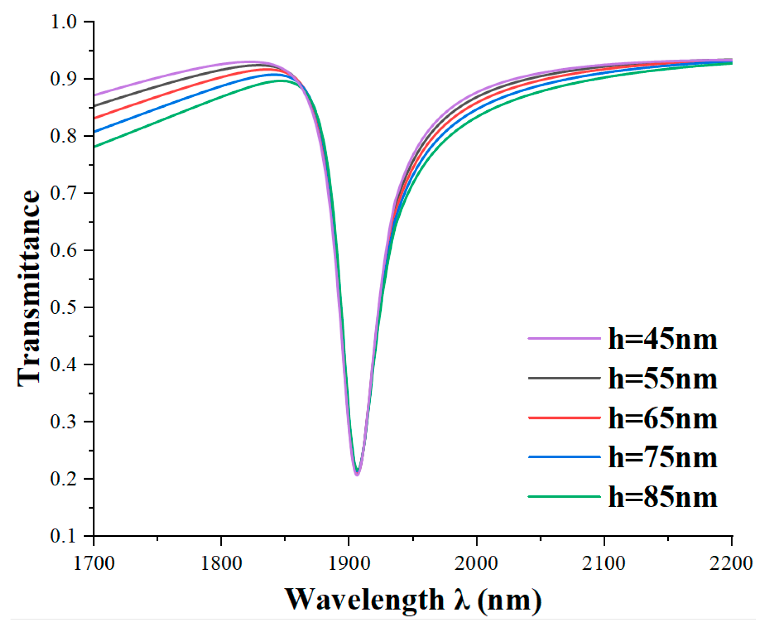
To assess the impact of changing the height of the reverse rectangular baffle on the sensor’s transmission performance, we incrementally raise it from 45 nm to 85 nm in 10 nm increments while keeping other parameters constant. The simulation results are depicted in
Figure 7.
Regardless of the variation in the height of the inverse rectangle, the position and transmittance of the Fano resonance remain largely stable. Furthermore, the Fano resonance curve exhibits distinct asymmetric features that become more pronounced by increasing the baffle height of the inverse rectangle. Finally, we explore the impact of the arc angle on the sensor’s transmission characteristics, maintaining all other parameters constant while incrementally increasing the arc angle φ from 60° to 80° and 2φ from 120° to 160°.
As shown in
Figure 8a, as the angle 2φ increases from 120° to 160°, a redshift occurs in the transmission spectrum, signifying an increase in the wavelength of transmitted light. At the same time, as shown in
Figure 8b, the sensor’s sensitivity undergoes a notable improvement. This indicates that within this angle range, enhancing the angle directly improves the sensor’s performance. However, upon exceeding 120°, the rate of improvement starts to decline, showing that beyond a specific threshold angle, further angle increases result in a gradual reduction in the enhancement of sensor sensitivity.
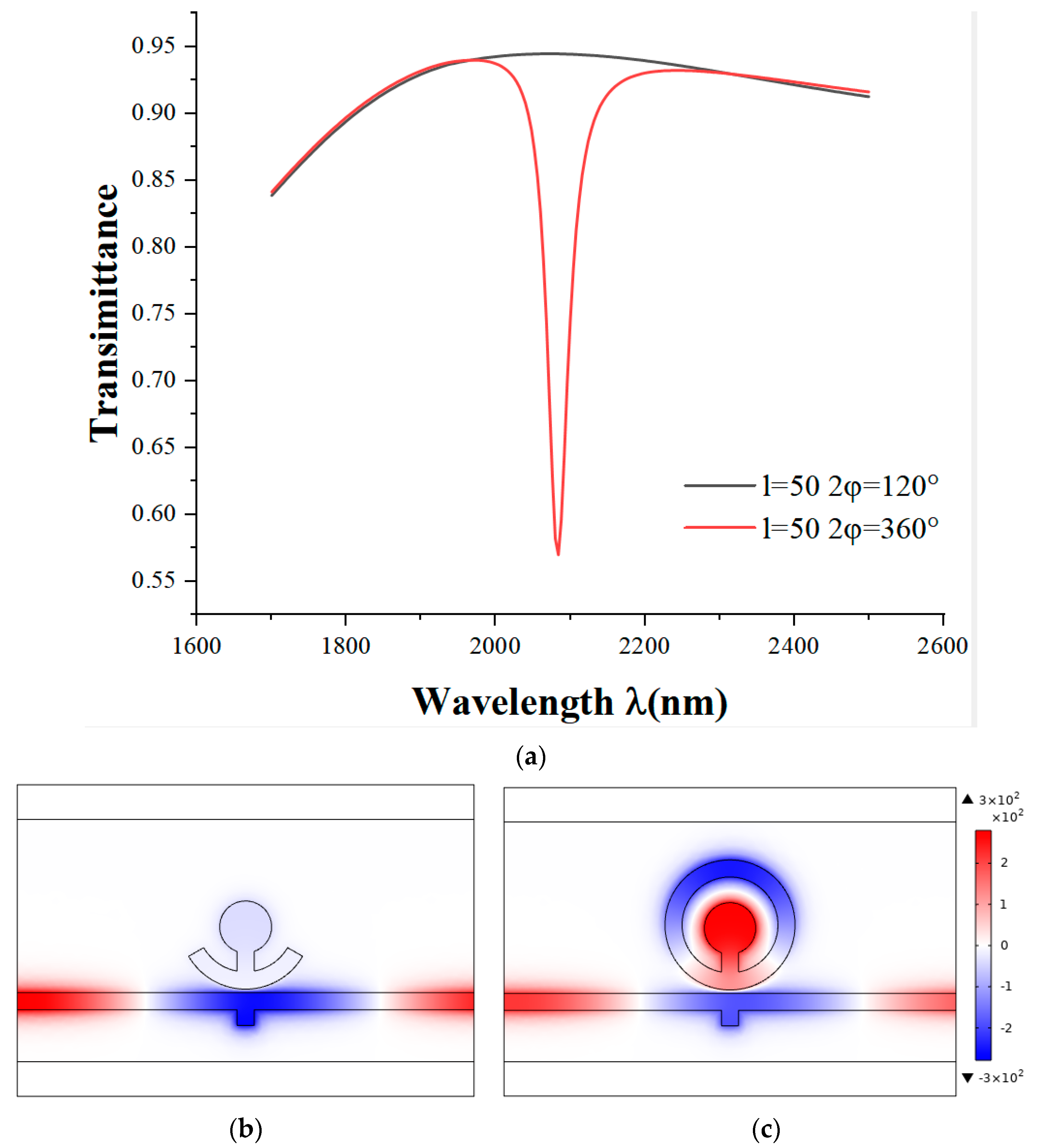
Subsequently, we explored the effects of adjusting the angle 2φ to 360° and setting l to 55 to form a ring. This was compared to merely adjusting l to 55. According to
Figure 9a, adjusting l alone results in a smooth curve and exhibits high transmission. When l is set to 55, forming a ring, and compared to only adjusting l to 55, the figure shows that adjusting l alone results in a transmission spectrum that becomes a smooth curve with high transmittance. This study further reveals that decreasing the length of l reduces the sensor’s sensitivity. However, with l at 55 and arc 2φ at 360°, forming a circle that encompasses the inner circle, transmittance decreases. Nonetheless, the arc’s completeness partially compensates for the reduction in transmittance. From the figure, we can also see that the magnetic field distributions of the two different structures are opposite. From
Figure 9b,c, we can also see that the magnetic field resonances of the two different structures are opposite. This suffices to demonstrate that the arc’s completeness is a significant factor influencing transmittance at a wavelength of 2082 nm.
4. The Application of this Structure in Hemoglobin Concentration
Red blood cells (RBCs) are often crucial indicators of related disorders. Erythrocytes, major blood cells, carry oxygen and carbon dioxide. In clinical practice, they serve as key indicators in routine blood tests, reflecting the body’s RBC production and aiding in diagnosing blood disorders. Hemoglobin (Hb), a special protein in RBCs, transports oxygen. Hemoglobin reference values differ by gender and age: men: 120–165 g/L, women: 110–150 g/L, newborns: 180–190 g/L, and children: 120–140 g/L (12–14 g/dL). Hemoglobin levels in newborns decrease with age, approaching adult levels. Slightly lower hemoglobin is normal in the elderly, during menstruation, or in mid-to-late pregnancy. Chemotherapy, HIV treatment, and conditions such as iron deficiency anemia, aplastic anemia, or thalassemia can reduce red blood cell production or increase loss or destruction, leading to low hemoglobin. Pathological factors such as severe vomiting, diarrhea, extensive burns, and conditions like chronic hypoadrenocorticism, uremia, or renal and hepatic cancer can result in high hemoglobin levels. Monitoring hemoglobin concentration allows for the immediate diagnosis of blood diseases and timely treatment, holding great clinical significance.
The relationship between Hb concentration and RI is defined as follows [
40]:
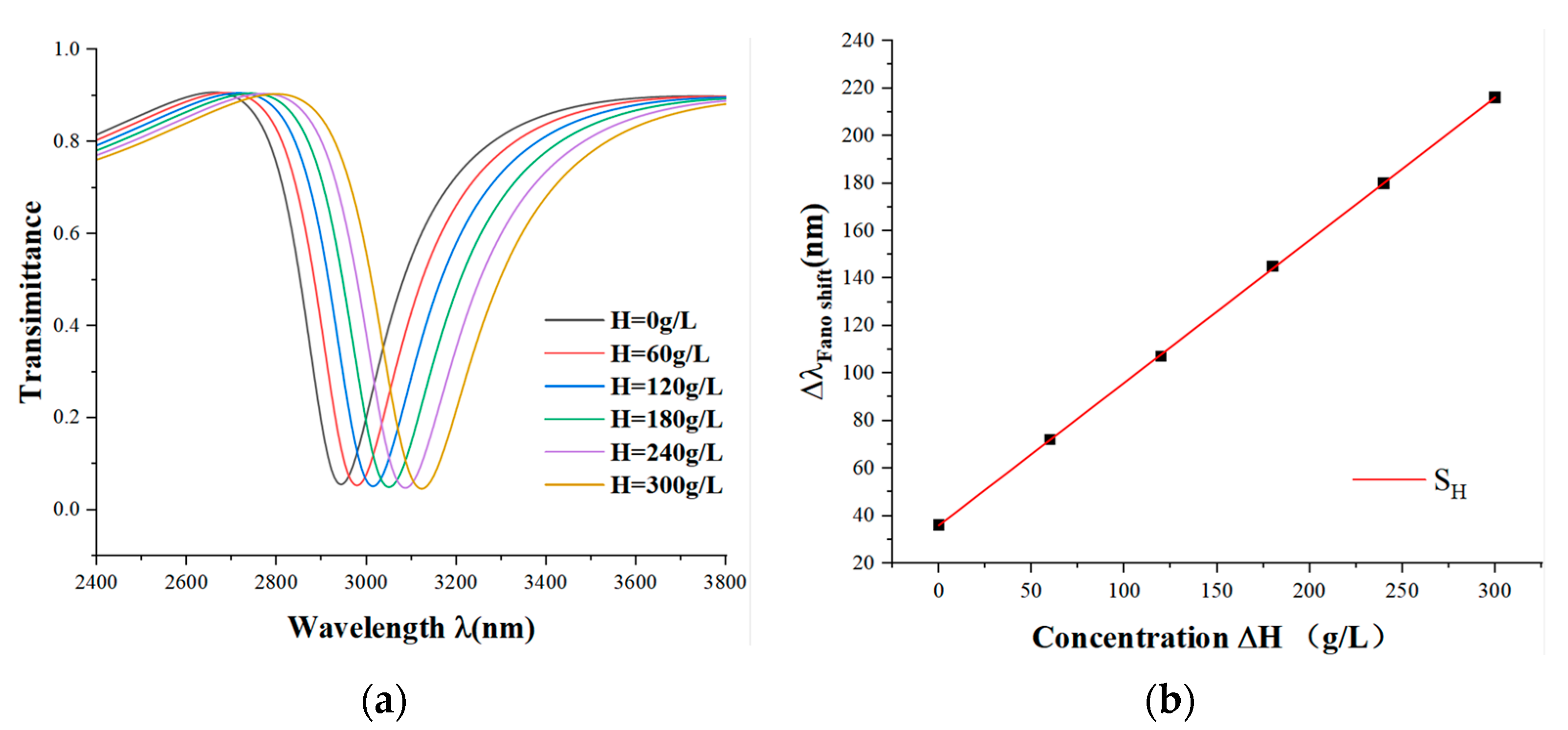
where
is 140 g/L, H represents the concentration to be measured, the test range spans from 0 to 300 g/L, and the step size is set at 60 g/L. The detection process entails injecting blood with varied hemoglobin concentrations into the sensor chamber, altering the medium’s refractive index. This results in spectral displacement. Sensor sensitivity is determined by the following equation:
where
represents the spectrum’s shift and
indicates changes in the concentration of blood red cells. Output spectra at various concentrations are depicted in
Figure 10a. The resonance trough’s wavelength changes in proportion to Hb concentration increases, with resonance wavelength spacing being 36 nm. The sensor sensitivity fitting is shown in
Figure 10b. The sensor sensitivity’s linear fit correlation coefficient exceeds 0.99, the sensor’s sensitivity is 0.6 nm·g/L, and the commercial spectral analyzer’s minimum resolution is 0.001 nm. The sensor provides more accurate concentration measurements than traditional spectroscopic or colorimeter methods. Compared with demand-labeled assay techniques (e.g., enzyme-linked immunosorbent assay—ELISA), a label-free assay is provided with fewer preprocessing steps [
41], demonstrating significant potential for advancing high-precision nanoscale hemoglobin concentration monitoring. However, surface plasma sensors are sensitive to ambient temperatures. Prolonged use in a clinical setting may place higher demands on the device’s durability and stability. Ensuring that the device maintains high performance and accuracy over repeated use may be a substantial obstacle for applications requiring large-scale screening, such as routine hemoglobin testing [
42].

 ,
, 


