Article

Influence of Efficient Thickness of Antireflection Coating Layer of HfO2 for Crystalline Silicon Solar Cell

1
School of Semiconductor and Chemical Engineering, Jeonbuk National University, Jeonju 54896, Korea
2
Graduate School of Integrated Energy-AI, Jeonbuk National University, Jeonju 54896, Korea
3
Myrveien 13, 9740 Lebesby Kommune, Norway
4
Department of Chemistry, College of Science and Arts and Promising Centre for Sensors and Electronic Devices (PCSED), Najran University, Najran 11001, Saudi Arabia
5
Department of Materials Science and Engineering, The Ohio State University, Columbus, OH 43210, USA
6
Department of Electrical Engineering, College of Engineering, Najran University, Najran 11001, Saudi Arabia
7
New and Renewable Energy Materials Development Center (NewREC), Jeonbuk National University, Jeonbuk 56332, Korea
*
Authors to whom correspondence should be addressed.
Visiting Professor at the Materials Science and Engineering, The Ohio State University, Columbus, OH 43210, USA.
Inorganics 2022, 10(10), 171; https://doi.org/10.3390/inorganics10100171
Submission received: 5 September 2022 / Revised: 3 October 2022 / Accepted: 8 October 2022 / Published: 12 October 2022
(This article belongs to the Special Issue 2D Materials for Optoelectronic Devices)

Abstract

:
Anti-reflective coating (ARC) layers on silicon (Si) solar cells usually play a vital role in the amount of light absorbed into the cell and protect the device from environmental degradation. This paper reports on the thickness optimization of hafnium oxide (HfO2) as an ARC layer for high-performance Si solar cells with PC1D simulation analysis. The deposition of the HfO2 ARC layer on Si cells was carried out with a low-cost sol-gel process followed by spin coating. The thickness of the ARC layer was controlled by varying the spinning speed. The HfO2 ARC with a thickness of 70 nm possessed the lowest average reflectance of 6.33% by covering wavelengths ranging from 400–1000 nm. The different thicknesses of HfO2 ARC layers were used as input parameters in a simulation study to explore the photovoltaic characteristics of Si solar cells. The simulation findings showed that, at 70 nm thickness, Si solar cells had an exceptional external quantum efficiency (EQE) of 98% and a maximum power conversion efficiency (PCE) of 21.15%. The thicknesses of HfO2 ARC considerably impacted the photovoltaic (PV) characteristics of Si solar cells, leading to achieving high-performance solar cells.

1. Introduction

The anti-reflective coating (ARC) layer on a solar cell helps the cell absorb more light and protects it from environmental damage [1,2]. In the absence of the ARC layer, the cells are naturally dark grey, but the color of the solar cells can be adjusted by altering the thickness of the ARC layer [3,4]. The major impediment to reaching high efficiency is optical losses from the front surface of the solar cell [5]. A thin layer of dielectric material called an ARC layer is applied to the illuminated surface of the solar cell to reduce optical losses caused by reflection and improve light transmission. This increases the current generation and the efficiency of the solar cell as a whole. The production of c-Si solar cells has utilized several ARC materials, including MgF2, a-SiNx, Si3N4, SiO2, SiO, SiO2-TiO2, Ta2O5, TiO2, ZnS, and so on [6,7]. Even though various materials are already employed, researchers continue searching for new and efficient ARC materials to improve the efficacy of solar cells.
In 2020, the report of the European Commission included hafnium (Hf) as a critical material. The oxide of Hf, like hafnium oxide (HfO2), includes its broad bandgap of ~5.6–5.8 eV and exhibits fabulous optical applications because it presents promising transmittance, weak reflective properties, good thermal stability (melting point is about 2780 °C), and a high induced laser damage threshold [8,9]. Because of its superior physical characteristics, such as strong corrosion resistance, great durability, scratch resistance, and good surface roughness, HfO2 has attracted great attention from researchers worldwide [10,11]. Other studies on the structural, morphological, and electrical characteristics of HfO2 thin films are also reported in the literature [12,13]. Due to its large range of dielectric constant, good mechanical characteristics, high bulk modulus, strong chemical stability, and high neutron absorption cross-section [14,15], it is a material that shows great potential for solar cell applications. Hafnium oxide (HfO2) is regarded as a viable material for several semiconductor industries as well as the energy sector because it is a stable known refractory material.
HfO2 and its derivatives have also enabled significant performance gains in a wide variety of energy storage, photovoltaic, high-power, and high-temperature devices, and so on [16]. The use of HfO2 is advantageous because it enhances the stability of solar cells by preventing further accumulation of native oxide [17]. HfO2 usually poses a large refractive index in the range of 1.85–2.1 and transferable absorption behavior. Due to their high transparency, HfO2 thin films can be employed as antireflective coatings for IR optical devices, space cameras, and night vision equipment [18]. The excellent properties of HfO2 films have been reported regarding the effect of deposition angle (in the case of sputtered films), antireflection potential, deposition substrate temperature, morphological characteristics, annealing effect on film characterizations, and so on [19]. HfO2, although a well-known optical material, has been investigated for its efficient uses in capacitors, sensors, ferroelectric materials, and so on [20]. HfO2 shows transparency in UV to mid-IR wavelengths. It is relatively uncommon in the literature for solution-based spin coating methods to be used to investigate HfO2 thin films for solar cell applications. The range of applications for such coatings is increased by its hydrophobic feature, which works in conjunction with its suitable optical properties [21,22]. Therefore, for future advancements in solar cells, it is crucial to get knowledge about such an appealing material prepared with a straightforward and affordable spin coating technique.
To study the optoelectrical characteristics of the solar cells, a variety of simulation tools are available, including Silvaco TCAD, AFROS-HET, Setfos, PC1D, OPAL2, AMPS-1D SCAP-1D, and so on [23]. Due to its quick computation time and simple user interface, PC1D simulation is frequently employed to mimic the properties of Si solar cells [24]. With a minimal reflectance of 0.3% at a wavelength of 580 nm, Kanmaz et al. deposited HfO2 as an AR layer on the silicon substrate which produced an average reflectance of 11.32% [25]. Nb2O5, as ARC was deposited on Si substrate by Shah et al., and the PC1D software, was used to predict the results, which showed the maximum PCE of over 17% with over 95% EQE [26]. After HfO2 was deposited, the average efficiency of the heterojunction with intrinsic thin-layer (HIT) solar cell increased from 18.21% to 20.75% according to Lee et al., who simulated the results using the online solver OPAL2 from PV Lighthouse [27].
In this study, a spin coating approach is used to deposit a sol-gel-derived precursor of HfO2 on Si solar cells at various spinning rates, and the thickness of the ARC layer is tuned by assessing the reflectance through ultraviolet diffuse reflectance spectroscopy (UV-DRS). Furthermore, the PC1D simulation software was applied for the characterization of PV properties and the simulated results have shown that the highest PCE of 21.15% and more than 98% EQE at 70 nm thickness of the ARC layer, which might be efficient for c-Si solar cells.

2. Experimental Details

2.1. Texturing of the Surface of the Silicon Wafer

An aqueous alkaline texturing solution (45% KOH + 4.4% hoplatex (TX-11) in DI water) was used to create the texture on a p-type c-Si wafer (16 cm2, 120 µm (thick), sheet resistance ~1–3 Ω/cm2). The c-Si wafer was given a homogeneous texture by immersing it in etching solutions for 20 min at 80 °C, followed by a thorough wash in deionized (DI) water with sonication for 10 min. To generate the phosphorus layer (as an n-type layer) over the p-type c-Si wafer, the cleaned, textured c-Si wafers were put horizontally into a diffusion furnace. For this, a phosphorus supply from the POCl3 gas source was immediately added to the furnace at 700–800 °C for 50 min. The n-p-n structure, which was made by the diffusion of phosphorous on both sides of a Si wafer having a sheet resistance of 70 Ω/□, was used. Finally, a 5% hydrofluoric acid (HF) solution treatment was employed to remove phosphorous silicate glass (PSG) from the surface of the p-n junction structure.

2.2. Preparation of Precursor and Deposition of ARC Layer

Before being dried in an oven, the textured Si wafer was first extensively cleaned with acetone and DI water under sonication for 15 min. The HfO2 precursor [1,25] was prepared by mixing 0.5 mg of hafnium (IV) chloride (HfCl4) in a 10 mL mixed solution of toluene and ethanol (5 mL of toluene + 5 mL ethanol). The resultant mixture was stirred for 2 h and kept for aging for 24 h at 298 K to stabilize the temperature before spin coating [1]. Before ARC layer deposition, a seed layer was formed on the top surface of a silicon wafer for the effective deposition of AR materials. A seed layer is needed for a nucleation process and the beginning of an induced preferential direction growth. A seed layer is also used to accommodate the lattice parameter between the substrate and the subsequent thin film for improving the adhesion [28]. To deposit the seed layer, 30% hydrogen peroxide (H2O2) solution was coated on the surface of a pre-cleaned textured Si wafer by spin coating at 2000 rpm for 30 s and was finally dried at 60 °C in an oven for 1 h.
A straightforward spin coating technique was employed to coat the HfO2 ARC layer on a Si wafer. By adjusting the spin coating rpm speeds (1000, 2000, and 3000 rpm) for 30 s, it was possible to control the thickness of the HfO2 layer that covered the textured Si wafer. The layer was then baked for 10 min at 60 °C to dry it off. The deposited HfO2 films were then further heated in air at 500 °C for 10 min at a temperature ramping rate of 5 °C/min to eliminate impurities from the coated surfaces [25]. Figure 1 depicts the conceptual framework for constructing the proposed HfO2 ARC layer-based Si solar cell.

2.3. Characterizations

Analytical, spectroscopic, and PV measurements were used to characterize the fabricated HfO2 ARC layer on silicon wafers. Field emission scanning electron microscopy (FE-SEM) (Hitachi 4800, Hitachi, Tokyo, Japan) was used to examine microstructure and surface morphology. XRD and photoluminescence (PL) spectroscopy were used to confirm the deposition of HfO2. The optical characteristics were examined by UV diffused reflectance spectroscopy (UV-DRS; Shimadzu MPC-3100, Shimadzu, Kyoto, Japan) using the wavelength range (400–1200 nm). By utilizing a 904 nm laser, the lifetimes including both surface and bulk lifetime of HfO2 coated c-Si wafers were determined. The HfO2 thicknesses and reflectance were used as input parameters in the PC1D simulation to determine the precise PV properties.

2.4. PC1D Simulating Tool

The University of New South Wales (UNSW) team developed the PC1D simulation software, which can be used to investigate the optoelectrical properties of solar cells [29]. The PC1D computer application is a popular numerical modeling program for c-Si solar cell simulation. Using a finite-element numerical method, it determines the linked nonlinear equations for carrier generation, recombination, and transport in semiconductor devices [30]. High computation rates, a large list of material and physical parameters, and a simple user interface are all advantages of using PC1D [31]. It offers a wide range of analysis possibilities in both the time and geographical domains [32]. The batch mode of PC1D enables users to swiftly undertake optimization studies for a single parameter rather than often adjusting the parameters. For each input parameter in the batch mode, the range, the number of different values, and the kind of variations (logarithmic or linear) must all be specified [31,32,33]. This software contains several library files for semiconductor materials, such as AlGaAs, a-Si, c-Si, Ge, GaAs, GIN, and InP, to name a few [34,35]. This simulation software was used to examine the optoelectrical properties of solar cells using important parameters such as semiconductor bandgap, device area, reflectance value, device thickness, dielectric constant, carrier density, etc. as input parameters. The PC1D simulator’s internal model was chosen from other factors, and Table 1 lists all of the input parameters for the tool.

3. Result and Discussion

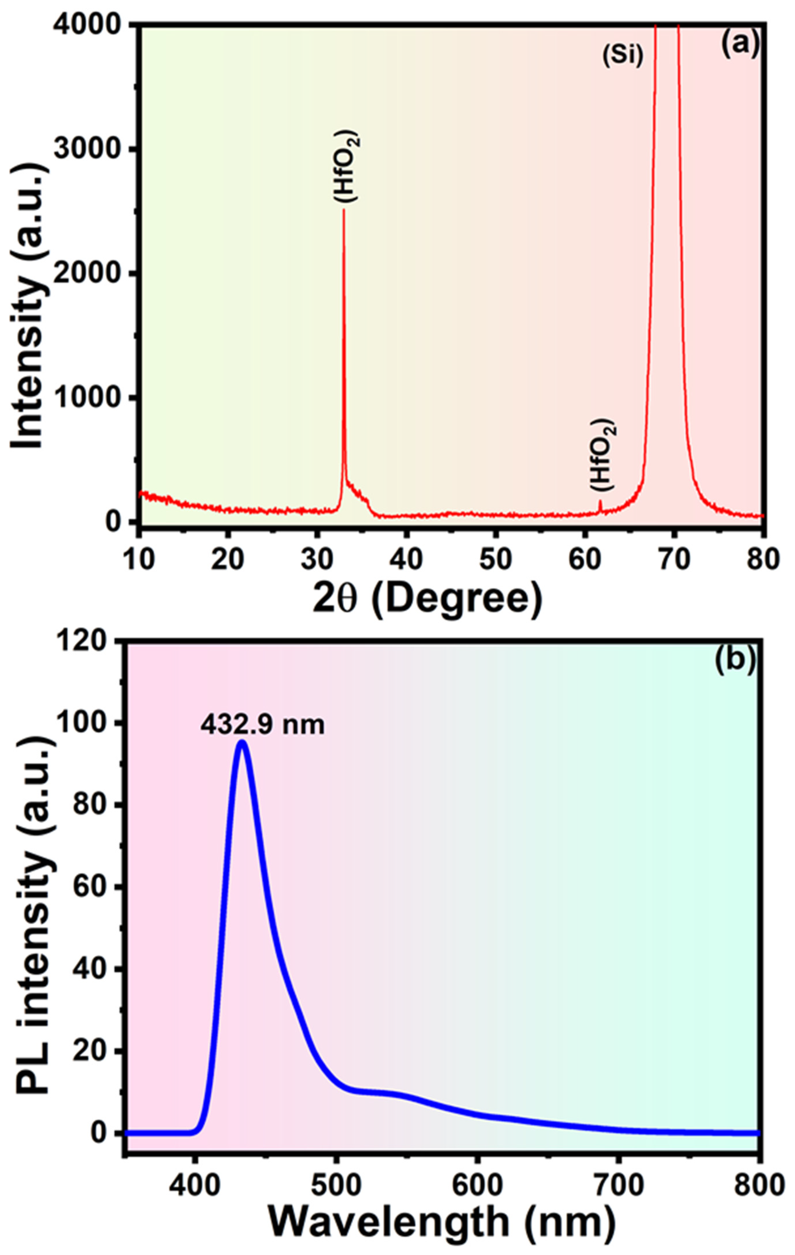
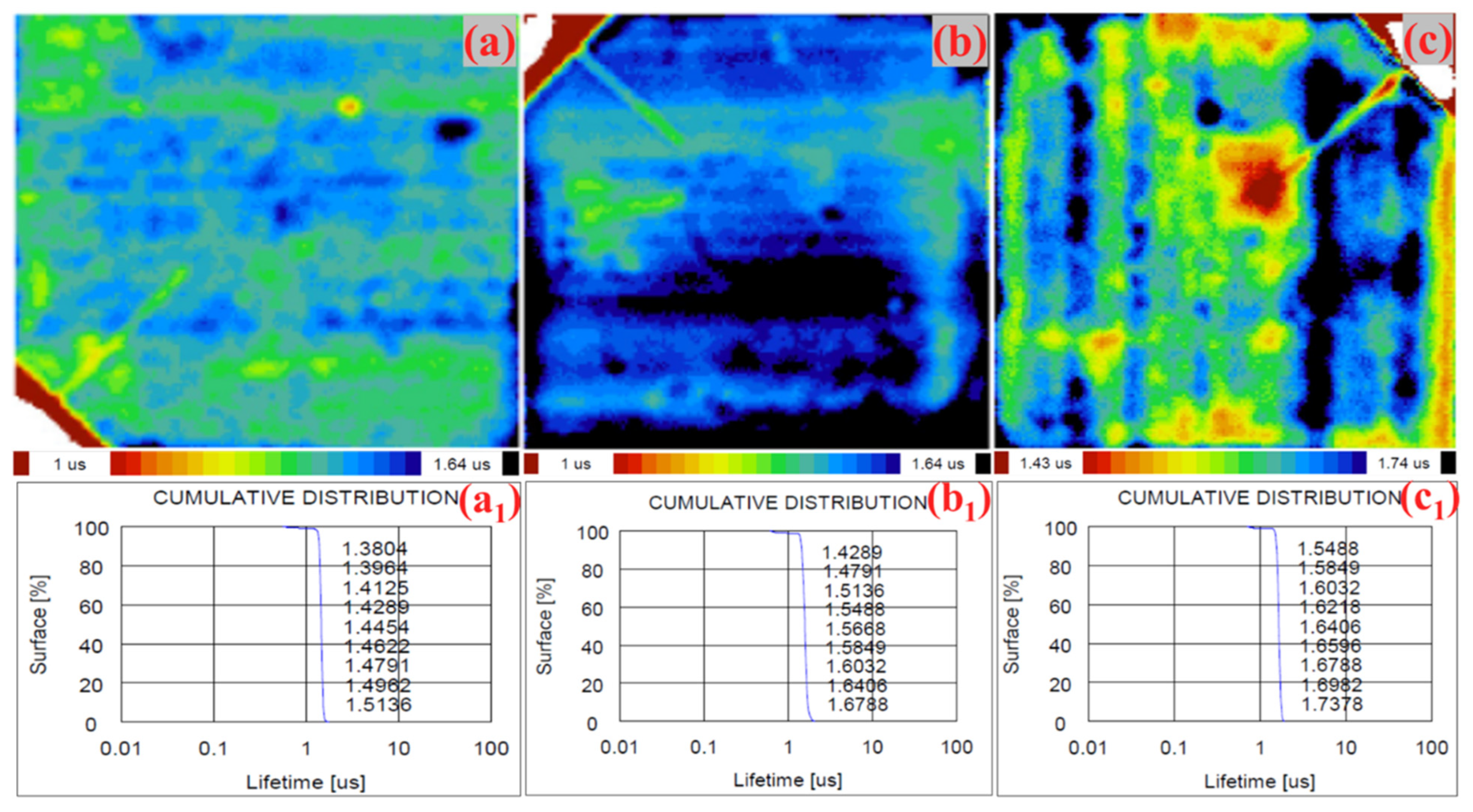
3.1. Crystallinity and Morphological Features

The XRD method was used to study the structural properties of the obtained HfO2 thin films. As illustrated in Figure 2a, the diffraction peaks of HfO2 are located at 31.95° (111) and 61.78° (311) in which the peak intensity at 32.95° is the strongest for the film deposited [36]. Additionally, the peak of Si is observed at 68.78°, indicating that the HfO2 layer was properly deposited on the Si wafer. With an emission peak at 432.9 nm, PL spectroscopy further supported the deposition of HfO2 on the Si wafer. It also attributed the Si-O emission near the surface to the surface state, or quantum-limited effect (QLE), as seen in Figure 2b [37].
A FESEM analysis was used to quantify the thickness of the HfO2 ARC layer on the textured Si wafer using the cross-sectional view as shown in Figure 3. At spinning speeds of 1000, 2000, and 3000 rpm, the observed thicknesses of HfO2 films were 80 nm, 70 nm, and 60 nm, respectively. Interestingly, at 2000 rpm, the HfO2 thickness of 70 nm on the textured c-Si wafer was improved and exhibits excellent optical, structural, and photovoltaic capabilities. The FE-SEM images revealed the uniform deposition of the HfO2 layer over the surface of the Si wafer (Figure 3d). For further evaluation of photovoltaic capabilities, the experimentally determined HfO2 layer thickness was used as one of the input parameters in the PC1D simulation tool.

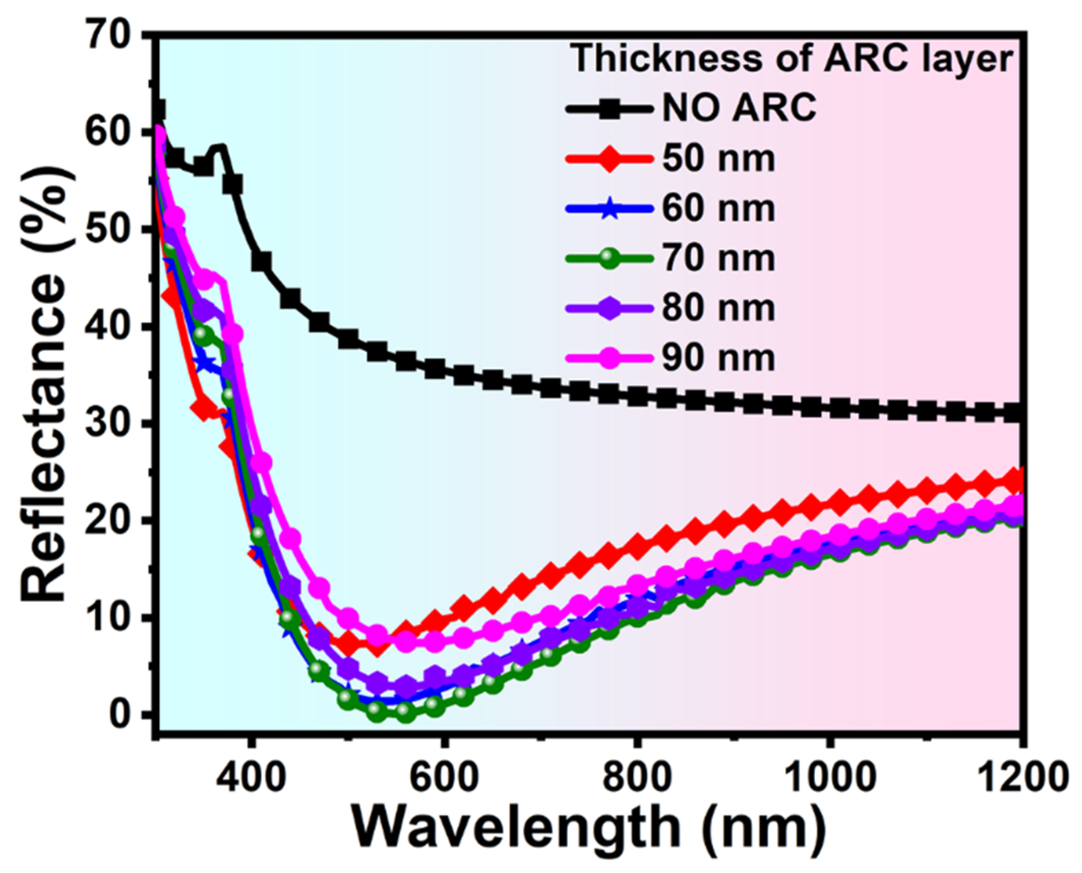
3.2. Optical Properties

The bulk lifetime can be determined by comprehending the recombination mechanisms in semiconductors including doped and undoped materials. The effective lifetime (τeff) of the minority carrier is often calculated by combining the lifetimes of the recombination mechanisms like band-to-band (radiative) recombination, Auger recombination, and Shockley–Read–Hall (SRH) via traps within the energy gap. The silicon solar cell’s surface and interior recombination lifetimes can be used to calculate τeff, as shown in the below equation [38];
1 τ e f f = 1 τ b + S f r o n t + S b a c k W
Sfront & Sback stand for the simplified version of the recombination generating over the front and back sides of the wafer, where W is the thickness of the silicon wafer. A possible way to estimate the surface lifetimes on the surface and bulk is with the lifetime mapping measurement of the c-Si wafer. Only bulk lifetime is taken into account because the front surface of the Si wafer may be passivated after HfO2 ARC deposition.
To understand the surface bulk charge carrier lifetime, the lifetime mapping images of the HfO2 ARC layer on a textured Si wafer with varied thicknesses have been examined [39]. In general, during the scanning of the Si wafer, the color changes define the minority carrier lifetimes. The HfO2 ARC layer on Si solar cells may be best applied at a thickness of 70 nm because it has the lowest surface lifetime value when compared to other thicknesses. As illustrated in Figure 4b, with an ARC layer-based Si wafer of 70 nm thickness, a reduction in the bulk lifetime from 1.6788 μs to 1.4289 μs is seen and manifests the lesser charge carriers, which may be advantageous for enhancing the optical characteristics. When compared to other samples, the HfO2 ARC layer on a Si solar cell has a surface cumulative distribution of lifetime that is optimized at 1.5538 μs, which results in a short lifespan for bulk charge carriers on Si wafers as seen in Figure 4b1. The optical behavior of ARC surfaces might be affected by the lifespan of charge carriers and their distribution.
To assess the reflectance at various HfO2 ARC layer thicknesses on the surface of the Si substrate, UV-DRS spectroscopy has been used. As shown in Figure 5a, the reflectance analysis findings showed that the average reflectance was 22.61% for bare silicon, 10.51% for textural silicon, and 7.44%, 6.33%, and 8.35% for the thickness of HfO2 layers 80, 70, and 60 nm, respectively, produced at 1000, 2000, and 3000 rpm. The reflectance values of the various ARC layer thicknesses that were measured during the experiment are strikingly close to the findings of simulations, which are depicted in Figure 6.
HfO2 ARC with 70 nm thickness at 2000 rpm showing minimum reflectance has been used to optimize the thickness of the HfO2 ARC layer. Due to this fact, ARC thickness is an odd integer multiple of the quarter wavelength which relates to the propagation inside the coating medium for a given frequency, and ARC thickness more effectively maintains the constructive interference condition [40]. Using reflectance data, the refractive indices and extinction coefficients for all of the HfO2 ARC layers on the Si substrate were calculated [41]. According to Figure 5b, the HfO2 layer, which has a thickness of 70 nm, has the maximum refractive index (n = 2.3), which is also advantageous for effective Si solar cells. Table 2 contains the values for the HfO2 layer thicknesses deposited on the Si substrate at the spinning rate. Therefore, a low reflectance HfO2 ARC material-based solar cell is ideal for producing effective solar cells.
To further define the photovoltaic parameters, it is important to have an accurate model, which explains the uniform distribution of surface resistance or sheet resistance over the substrate [42]. By assisting the dispersed series resistance interconnecting gridlines and so affecting the overall series resistance of a solar cell, the sheet resistance of Si substrate can affect the Isc, FF, and consequently the efficiency of a solar cell. Thus, the sheet resistance should be optimized to achieve an excellent ohmic contact [43]. The sheet resistance increases with decreases in the thickness of HfO2 layers on the silicon substrate as shown in Figure 7a. The maximum sheet resistance ~144.78 Ω/□ is recorded at a thickness of 70 nm (deposited at 2000 rpm), which is also beneficial to develop efficient solar cells.
The transmittance is a crucial optical property for silicon solar cells, a higher transmittance is needed for applications in optical devices to reduce light intensities. The number of nanoparticles on the thin films is increased with reduced particle size causing light intensity loss at these boundaries and absorption of light increases [44]. The HfO2 film deposited on the silicon wafer has a transmittance of more than 80% at a large wavelength range and a decrease in transmittance as the wavelength of light increases as shown in Figure 7b. Additionally, the measured absorbance value is ~0.2 in the range of 500–800 nm of optimized thicknesses at 70 nm of ARC layer compensates with the value of transmittance as shown in Figure 8. These optical properties are appropriate for high-performance and efficient c-Si solar cells.

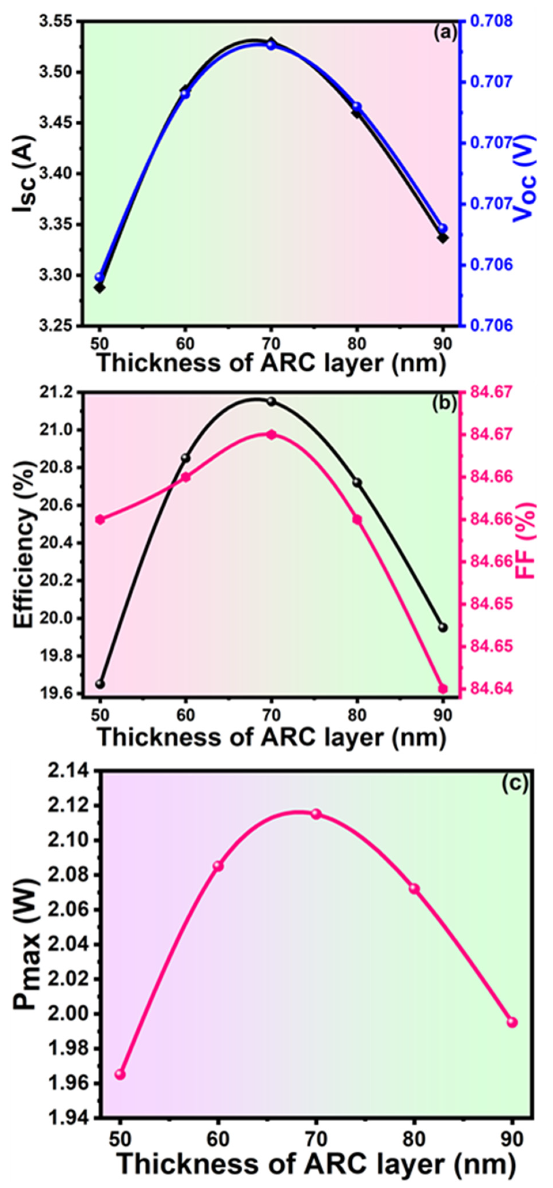
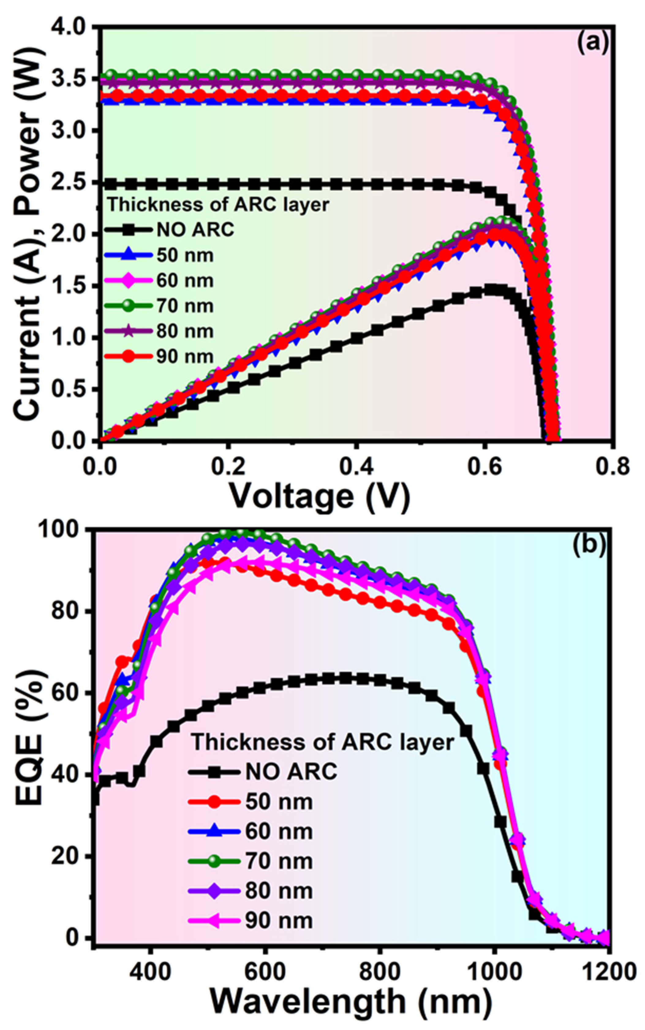
3.3. Photovoltaic Properties

The characteristics of solar cells such as Isc, Voc, PCE, FF, and Pmax increase as the ARC layer thickness increases, up to 70 nm, and then starts to decrease (Figure 9). This is because, at 70 nm, the thickness of ARC more effectively maintains the state of constructive interference [45]. It is not feasible to penetrate light into the surface of a solar cell because light rays reflecting off the ARC’s top and bottom surfaces have similar paths, with a path difference of less than λ/4 [46]. Because ARC holds the condition of destructive interference more effectively, the reflectivity declines linearly after more than 70 nm of ARC thickness. The condition of destructive interference is perfectly achieved and exhibits the lowest reflectance at an ARC layer thickness of 70 nm. The top values of Isc = 3.52 A, Voc = 0.707 V, PCE = 21.15%, FF = 84.67%, and Pmax = 2.11 W have been observed at optimized ARC thickness of 70 nm as shown in Figure 9a–c.
The concentration of light affects electrical parameters such as Isc, Voc, Pmax, PCE, and FF of the c-Si solar cell [47]. Figure 10 presented that the PV parameters like Isc, Voc, Pmax, PCE, and FF increase with the increase of illumination light intensity. The maximum value of I = 3.52 A and P = 3.2 W have been observed at standard conditions i.e., the light intensity of 0.1 W/cm2 as shown in Figure 10a. The top values of Isc = 3.52 A, Voc = 0.708 V, Pmax = 2.11 W, and PCE = 21.15% have been observed at standard condition (Light Intensity = 0.1 W/cm2) as shown in Figure 10b,c.
The development of efficient solar cells highly depends on the I-V curve. The maximum I = 3.52 A, and Pmax = 2.11 W has been observed at an ideal thickness of 70 nm HfO2 ARC layer, as illustrated in Figure 11a. This is in contrast to other ARC layer thicknesses in c-Si solar cells. The largest photocurrent that solar cells might produce has now been created due to an increase in photon absorption efficiency. The EQE is a measurement of the ratio of incident photons to photo-generated carriers as a function of wavelength [48]. The EQE of ARC-based Si solar cells has been demonstrated to increase gradually with bare (no ARC layer) silicon, as displayed in Figure 11b.
As illustrated in Figure 11b, different ARC layer thicknesses from 50 nm to 90 nm were used to study the performance of ARC layer-based solar cells in terms of EQE. For ARC layer-based c-Si solar cells, the greatest EQE at optimum thickness at 70 nm provided nearly 98% at the range of wavelength 300–1000 nm. Among all ARC layer thicknesses, the HfO2 ARC layer-based solar cell exhibits the best EQE with a 70 nm thickness. Table 2 provides an overview of the experimental and simulation PV characteristics of silicon solar cells based on ARC technology. Table 3 summarizes the electrical characteristics of reported ARC material-based solar cells. HfO2 ARC-based solar cells performed better than others did when these electrical properties were compared, and they may be ideal for producing the proposed solar cells. The parameters of the HfO2 ARC-based solar cell predicted by the PC1D modeling program are validated by this comparative investigation of the proposed solar cell.

4. Conclusions

In summary, HfO2 ARC with different thicknesses was deposited by a cost-effective sol-gel process followed by spin coating to investigate the PV features of HfO2 ARC-based silicon solar cells. An approach based on simulation was employed to examine the optoelectrical properties of the HfO2 ARC layer-based c-Si solar cell. With an HfO2 ARC thickness of 70 nm, the lowest average reflectance of the average reflectance of ~6.33% was achieved which is lowered to other ARC thicknesses. To describe the PV parameters of c-Si solar cells, several ARC thicknesses were used as input parameters. The topmost PCE of 21.15% according to the simulated results is seen at an ARC layer thickness of 70 nm. It was discovered that the HfO2 ARC layer’s optimal thickness (70 nm) had the maximum performance, Isc, and EQE, which was 98%. The use of low-cost HfO2 ARC layer-based high-performance Si solar cells would be made possible by a simulation study on the optimization of ARC thicknesses for Si solar cells.

Author Contributions

This work is the collaborative development of all the authors. D.K.S.: original draft, conceptualization, methodology, formal analysis. D.K.: data curation, investigation, software, validation. H.A.: editing—draft, writing—review, investigation. A.U.: editing—final draft, investigation. M.S.A.: investigation, data curation, writing—review, and editing. O.-B.Y.: funding acquisition, writing—review, supervision, and editing. All authors have read and agreed to the published version of the manuscript.

Funding

This research was supported by Jeonbuk National University, South Korea.

Institutional Review Board Statement

Not applicable.

Informed Consent Statement

Not applicable.

Data Availability Statement

Not applicable.

Acknowledgments

This work was supported by the “Human Resources Program in Energy Technology” of the Institute of Energy Technology Evaluation and Planning (KETEP) and granted financial resources from the Ministry of Trade, Industry & Energy, Republic of Korea (Project No.: 20204010600470). This work was also supported by the National Research Foundation of Korea (NRF) grant funded by the Korea government (MSIT, Project No. 2022M3J7A1066428).

Conflicts of Interest

The authors declare no conflict of interest.

References

  1. Sarkın, A.S.; Ekren, N.; Sağlam, Ş. A review of anti-reflection and self-cleaning coatings on photovoltaic panels. Sol. Energy 2020, 199, 63–73. [Google Scholar] [CrossRef]
  2. Tiwari, R.; Sadanand; Dubey, P.; Lohia, P.; Dwivedi, D.K.; Fouad, H.; Akhtar, M.S. Simulation Engineering in Quantum Dots for Efficient Photovoltaic Solar Cell Using Copper Iodide as Hole Transport Layer. J. Nanoelectron. Optoelectron. 2021, 16, 1897–1904. [Google Scholar] [CrossRef]
  3. Hu, R.; Li, Y.; Que, Z.; Zhai, S.; Feng, Y.; Chu, L.; Li, X. Low Temperature VOx Hole Transport Layer for Enhancing the Performance of Carbon-Based Perovskite Solar Cells. J. Nanoelectron. Optoelectron. 2021, 16, 273–280. [Google Scholar] [CrossRef]
  4. Shah, D.K.; Son, Y.-H.; Lee, H.-R.; Akhtar, M.S.; Kim, C.Y.; Yang, O.-B. A stable gel electrolyte based on poly butyl acrylate (PBA)-co-poly acrylonitrile (PAN) for solid-state dye-sensitized solar cells. Chem. Phys. Lett. 2020, 754, 137756. [Google Scholar] [CrossRef]
  5. Battaglia, C.; Cuevas, A.; De Wolf, S. High-efficiency crystalline silicon solar cells: Status and perspectives. Energy Environ. Sci. 2016, 9, 1552–1576. [Google Scholar] [CrossRef] [Green Version]
  6. Shah, D.K.; KC, D.; Akhtar, M.S.; Kim, C.Y.; Yang, O.-B. Vertically Arranged Zinc Oxide Nanorods as Antireflection Layer for Crystalline Silicon Solar Cell: A Simulation Study of Photovoltaic Properties. Appl. Sci. 2020, 10, 6062. [Google Scholar] [CrossRef]
  7. Hwang, J.Y.; Kim, I.T.; Choi, H.W. Characteristics of Perovskite Solar Cells with ZnGa2O4: Mn Phosphor Mixed Polyvinylidene Fluoride Down-Conversion Layer. J. Nanoelectron. Optoelectron. 2021, 16, 855–860. [Google Scholar] [CrossRef]
  8. KC, D.; Shah, D.K.; Alanazi, A.M.; Akhtar, M.S.; Kim, C.Y.; Yang, O.-B. Impact of Different Antireflection Layers on Cadmium Telluride (CdTe) Solar Cells: A PC1D Simulation Study. J. Electron. Mater. 2021, 50, 2199–2205. [Google Scholar] [CrossRef]
  9. Curtis, C.E.; Doney, L.M.; Johnson, J.R. Some Properties of Hafnium Oxide, Hafnium Silicate, Calcium Hafnate, and Hafnium Carbide. J. Am. Ceram. Soc. 1954, 37, 458–465. [Google Scholar] [CrossRef]
  10. Zhao, X.; Vanderbilt, D. First-principles study of structural, vibrational, and lattice dielectric properties of hafnium oxide. Phys. Rev. B 2002, 65, 233106. [Google Scholar] [CrossRef]
  11. Al-Kuhaili, M.F. Optical properties of hafnium oxide thin films and their application in energy-efficient windows. Opt. Mater. 2004, 27, 383–387. [Google Scholar] [CrossRef]
  12. Gritsenko, V.A.; Perevalov, T.V.; Islamov, D.R. Electronic properties of hafnium oxide: A contribution from defects and traps. Phys. Rep. 2016, 613, 1–20. [Google Scholar] [CrossRef]
  13. Kukli, K.; Ritala, M.; Sundqvist, J.; Aarik, J.; Lu, J.; Sajavaara, T.; Hårsta, A. Properties of hafnium oxide films grown by atomic layer deposition from hafnium tetraiodide and oxygen. J. Appl. Phys. 2002, 92, 5698–5703. [Google Scholar] [CrossRef]
  14. Field, J.A.; Luna-Velasco, A.; Boitano, S.A.; Shadman, F.; Ratner, B.D.; Barnes, C.; Sierra-Alvarez, R. Cytotoxicity and physicochemical properties of hafnium oxide nanoparticles. Chemosphere 2011, 84, 1401–1407. [Google Scholar] [CrossRef] [PubMed]
  15. Dole, S.L.; Hunter, O.; Wooge, C.J. Elastic Properties of Monoclinic Hafnium Oxide at Room Temperature. J. Am. Ceram. Soc. 1977, 60, 488–490. [Google Scholar] [CrossRef]
  16. Kukli, K.; Aarik, J.; Ritala, M.; Uustare, T.; Sajavaara, T.; Lu, J.; Leskelä, M. Effect of selected atomic layer deposition parameters on the structure and dielectric properties of hafnium oxide films. J. Appl. Phys. 2004, 96, 5298–5307. [Google Scholar] [CrossRef]
  17. Lee, B.H.; Kang, L.; Qi, W.-J.; Nieh, R.; Jeon, Y.; Onishi, K.; Lee, J.C. Ultrathin hafnium oxide with low leakage and excellent reliability for alternative gate dielectric application. In International Electron Devices Meeting 1999; Technical Digest (Cat. No. 99CH36318); IEEE: Piscataway, NJ, USA, 1999. [Google Scholar]
  18. Robertson, J. High dielectric constant oxides. Eur. Phys. J. Appl. Phys. 2004, 28, 265–291. [Google Scholar] [CrossRef] [Green Version]
  19. He, S.; Lu, H.; Li, B.; Zhang, J.; Zeng, G.; Wu, L.; Feng, L. Study of CdTe/ZnTe composite absorbing layer deposited by pulsed laser deposition for CdS/CdTe solar cell. Mater. Sci. Semicond. Process. 2017, 67, 41–45. [Google Scholar] [CrossRef]
  20. Tsui, K.-H.; Lin, Q.; Chou, H.; Zhang, Q.; Fu, H.; Qi, P.; Fan, Z. Low-Cost, Flexible, and Self-Cleaning 3D Nanocone Anti-Reflection Films for High-Efficiency Photovoltaics. Adv. Mater. 2014, 26, 2805–2811. [Google Scholar] [CrossRef]
  21. Khan, S.B.; Zhang, Z.; Lee, S.L. Annealing influence on optical performance of HfO2 thin films. J. Alloys Compd. 2019, 152552. [Google Scholar] [CrossRef]
  22. Nistor, C.L.; Mihaescu, C.I.; Bala, D.; Gifu, I.C.; Ninciuleanu, C.M.; Burlacu, S.G.; Petcu, C.; Vladu, M.-G.; Ghebaur, A.; Stroea, L.; et al. Novel Hydrophobic Nanostructured Antibacterial Coatings for Metallic Surface Protection. Coatings 2022, 12, 253. [Google Scholar] [CrossRef]
  23. Shah, D.K.; KC, D.; Muddassir, M.; Akhtar, M.S.; Kim, C.Y.; Yang, O.-B. A simulation approach for investigating the performances of cadmium telluride solar cells using doping concentrations, carrier lifetimes, thickness of layers, and band gaps. Sol. Energy 2021, 216, 259–265. [Google Scholar] [CrossRef]
  24. Shah, D.K.; KC, D.; Kim, T.-G.; Akhtar, M.S.; Kim, C.Y.; Yang, O.-B. Influence of minority charge carrier lifetime and concentration on crystalline silicon solar cells based on double antireflection coating: A simulation study. Opt. Mater. 2021, 121, 111500. [Google Scholar] [CrossRef]
  25. Kanmaz, I.; Mandong, A.M.; Uzum, A. Solution-based hafnium oxide thin films as potential antireflection coating for silicon solar cells. J. Mater. Sci. Mater. Electron. 2020, 31, 7. [Google Scholar] [CrossRef]
  26. Shah, D.K.; KC, D.; Kim, T.-G.; Akhtar, M.S.; Kim, C.Y.; Yang, O.-B. In-search of efficient antireflection layer for crystalline silicon Solar cells: Optimization of the thickness of Nb2O5 thin layer. Eng. Sci. 2022, 18, 243–252. [Google Scholar] [CrossRef]
  27. Lee, D.W.; Bhopal, M.F.; Lee, S.H.; Lee, A.R.; Kim, H.J.; Rehman, M.A.; Lee, S.H. Effect of additional HfO2 layer deposition on heterojunction c-Si solar cells. Energy Sci. Eng. 2018, 6, 706–715. [Google Scholar] [CrossRef] [Green Version]
  28. Son, D.-Y.; Bae, K.-H.; Kim, H.-S.; Park, N.-G. Effects of Seed Layer on Growth of ZnO Nanorod and Performance of Perovskite Solar Cell. J. Phys. Chem. C 2015, 119, 10321–10328. [Google Scholar] [CrossRef]
  29. KC, D.; Shah, D.K.; Akhtar, M.S.; Park, M.; Kim, C.Y.; Yang, O.-B.; Pant, B. Numerical Investigation of Graphene as a Back Surface Field Layer on the Performance of Cadmium Telluride Solar Cell. Molecules 2021, 26, 3275. [Google Scholar] [CrossRef]
  30. Hashmi, G.; Rashid, M.J.; Mahmood, Z.H.; Hoq, M.; Rahman, M. Investigation of the impact of different ARC layers using PC1D simulation: Application to crystalline silicon solar cells. J. Theor. Appl. Phys. 2018, 12, 327–334. [Google Scholar] [CrossRef] [Green Version]
  31. Haug, H.; Olaisen, B.R.; Nordseth, Ø.; Marstein, E.S. A Graphical User Interface for Multivariable Analysis of Silicon Solar Cells Using Scripted PC1D Simulations. Energy Procedia 2013, 38, 1876–6102. [Google Scholar] [CrossRef]
  32. Huang, H.; Lv, J.; Bao, Y.; Xuan, R.; Sun, S.; Sneck, S.; Li, S.; Modanese, C.; Savin, H.; Wang, A.; et al. Data of the recombination loss mechanisms analysis on Al2O3 PERC cell using PC1D and PC2D simulations. Data Brief 2017, 11, 27–31. [Google Scholar] [CrossRef]
  33. Yuan, M.; Wang, Z.; Zhang, G. Photoelectric Conversion Performance of Composite Perovskite Solar Cell Device and Its Application in Photovoltaic Building. J. Nanoelectron. Optoelectron. 2021, 16, 1492–1500. [Google Scholar] [CrossRef]
  34. KC, D.; Shah, D.K.; Shrivastava, A. Computational study on the performance of zinc selenide as window layer for efficient GaAs solar cell. Mater. Today Proc. 2022, 49, 2580–2583. [Google Scholar]
  35. Naim, H.; Shah, D.K.; Bouadi, A.; Siddiqui, M.R.; Akhtar, M.S.; Kim, C.Y. An in-depth optimization of thickness of base and emitter of ZnO/Si heterojunction based crystalline silicon solar Cell: A simulation method. J. Electron. Mater. 2022, 51, 586–593. [Google Scholar] [CrossRef]
  36. Wiatrowski, A.; Obstarczyk, A.; Mazur, M.; Kaczmarek, D.; Wojcieszak, D. Characterization of HfO2 Optical Coatings Deposited by MF Magnetron Sputtering. Coatings 2019, 9, 106. [Google Scholar] [CrossRef] [Green Version]
  37. Dai, D.; Guo, X.; Fan, J. Identification of luminescent surface defect in SiC quantum dots. Appl. Phys. Lett. 2015, 106, 053115. [Google Scholar] [CrossRef]
  38. Available online: https://www.pveducation.org/pvcdrom/characterisation/bulk-lifetime (accessed on 29 August 2022).
  39. Hossain, M.A.; Khoo, K.T.; Cui, X.; Poduval, G.; Zhang, T.; Li, X.; Hoex, B. Atomic layer deposition enabling higher efficiency solar cells: A review. Nano Mater. Sci. 2019, 2, 204–226. [Google Scholar] [CrossRef]
  40. Shah, D.K.; KC, D.; Parajuli, D.; Akhtar, M.S.; Kim, C.Y.; Yang, O.-B. A Computational Study of Carrier lifetime, Doping Concentration, and Thickness of Window layer for GaAs Solar Cell based on Al2O3 antireflection layer. Sol. Energy 2022, 234, 330–337. [Google Scholar] [CrossRef]
  41. Shah, D.K.; Choi, J.; KC, D.; Akhtar, M.S.; Kim, C.Y.; Yang, O.-B. Refined optoelectronic properties of silicon nanowires for improving photovoltaic properties of crystalline solar cells: A simulation study. J. Mater. Sci. Mater. Electron. 2021, 32, 2784–2795. [Google Scholar] [CrossRef]
  42. Chen, N.; Tate, K.; Ebong, A. Generalized analysis of the impact of emitter sheet resistance on silicon solar cell performance. Jpn. J. Appl. Phys. 2015, 54, 08KD20. [Google Scholar] [CrossRef]
  43. Diao, X.F.; Gao, L.K.; Xie, Y.; Tang, T.Y.; Tang, Y.L. Ferromagnetic and Antiferromagnetic Properties of Perovskite Solar Cell Materials. J. Nanoelectron. Optoelectron. 2021, 16, 434–443. [Google Scholar] [CrossRef]
  44. Joung, Y.-H.; Kang, S.-J. Effects of Working Pressure on Structural and Optical Properties of HfO2 Thin Films. J. Korea Inst. Electron. Commun. Sci. 2017, 12, 1019–1026. [Google Scholar]
  45. Durmaz, Z.; Husein, S.; Saive, R. Thin silicon interference solar cells for targeted or broadband wavelength absorption enhancement. Opt. Express 2021, 29, 4324–4337. [Google Scholar] [CrossRef]
  46. Ushasree, P.M.; Bora, B. Chapter 1: Silicon Solar Cells. In Solar Energy Capture Materials; RSC Publishing: Piccadilly, London, UK, 2019; pp. 1–55. [Google Scholar]
  47. Available online: https://www.pveducation.org/pvcdrom/solar-cell-operation/fill-factor (accessed on 29 August 2022).
  48. Han, H.-V.; Lin, C.-C.; Tsai, Y.-L.; Chen, H.-C.; Chen, K.-J.; Yeh, Y.-L.; Yu, P. A Highly Efficient Hybrid GaAs Solar Cell Based on Colloidal-Quantum-Dot-Sensitization. Sci. Rep. 2014, 4, 5734. [Google Scholar] [CrossRef] [PubMed] [Green Version]
  49. Alnuaimi, A.; Almansouri, I.; Saadat, I.; Nayfeh, A. High performance graphene-silicon Schottky junction solar cells with HfO2 interfacial layer grown by atomic layer deposition. Sol. Energy 2018, 164, 174–179. [Google Scholar] [CrossRef]
  50. Geng, H.; Lin, T.; Letha, A.J.; Hwang, H.-L.; Kyznetsov, F.A.; Smirnova, T.P.; Kaichev, V.V. Advanced passivation techniques for Si solar cells with high-κ dielectric materials. Appl. Phys. Lett. 2014, 105, 123905. [Google Scholar] [CrossRef]
Figure 1. Illustration of the proposed framework for constructing the HfO2 ARC layer-based c-Si solar cell.
Inorganics 10 00171 g001
Figure 2. (a) XRD patterns and (b) Photoluminescence spectrum of HfO2 ARC layer-based c-Si solar cell.
Inorganics 10 00171 g002
Figure 3. FE-SEM images of HfO2 ARC layer-deposited at rpm (a) 1000, (b) 2000, (c) 3000, and (d) 2000 on the c-Si substrate.
Inorganics 10 00171 g003
Figure 4. Analysis of lifetime surface mapping images and cumulative distribution of lifetime of the surface of the HfO2 layer deposited at spinning rate rpm (a,a1) 1000 (b,b1) 2000 (c,c1) 3000 for c-Si solar cell.
Inorganics 10 00171 g004
Figure 5. UV-DRS spectra in (a) reflectance mode and their corresponding (b) refractive index of HfO2 ARC layer-based c-Si solar cell.
Inorganics 10 00171 g005
Figure 6. Simulated reflectance analysis of HfO2 ARC layer-based c-Si solar cell.
Inorganics 10 00171 g006
Figure 7. Analysis of (a) Sheet resistance (b) Transmittance of HfO2 ARC layer-based c-Si solar cell.
Inorganics 10 00171 g007
Figure 8. Absorbance analysis of HfO2 ARC layer-based c-Si solar cell.
Inorganics 10 00171 g008
Figure 9. Plots of (a) Isc & Voc (b) PCE & FF (c) Pmax with a thickness of ARC layer-based c-Si solar cell.
Inorganics 10 00171 g009
Figure 10. Analysis of (a) I, P-V characteristic (b) Isc &Voc (c) Pmax & Efficiency with the different light intensity of HfO2 ARC layer-based c-Si solar cell.
Inorganics 10 00171 g010
Figure 11. Analysis of (a) I, P-V characteristic (b) External Quantum efficiency of ARC layer-based c-Si solar cell.
Inorganics 10 00171 g011
Table 1. Simulation parameters used in PC1D tool for HfO2 ARC layer-based c-Si solar cell.
ParametersValue
Device area100 cm2
Front surface texture depth3 μm
The thickness of the Si solar cell150 μm
Dielectric constant11.9
Energy bandgap1.124 eV
Background doping p-type5 × 1016 cm−3
First front diffusion n-type3 × 1018 cm−3
Refractive index3.42
Excitation modeTransient
Temperature25 °C
Other parametersAn internal model of PC1D
Primary light sourceAM 1.5D spectrum
Bulk recombination10 μs
Constant intensity0.1 W/cm2
Table 2. Photovoltaic parameters of HfO2 ARC-based c-Si solar cell.
Thickness of
ARC Layer
(nm)
Average ReflectanceRefractive IndexIsc
(A)
Voc
(V)
Pmax
(W)
FF
(%)
Efficiency
(%)
ExperimentalSimulationExperimentalSimulation
Bare Si22.6136.121.52--2.280.6421.2269.8012.27
Texture Si10.51--1.88------------
50--15.76--2.703.280.7051.96584.6619.65
607.4411.272.142.283.480.7072.08584.6420.85
706.339.452.302.953.520.7072.11584.6721.15
808.3511.802.041.703.460.7072.07284.6620.72
90--14.85--1.523.330.7062.99584.6419.95
Table 3. A summary of reported PV parameters of HfO2 ARC layer-based c-Si solar cell.
Types of Solar CellIsc
(A)
Voc
(V)
FF
(%)
Efficiency
(%)
References
Graphene/HfO2/Si3.340.45056.09.10[49]
HfO2/Si3.850.72374.520.75[27]
HfO2/Si3.850.72073.620.50[27]
HfO2/Si3.630.73067.115.54[50]
HfO2/Si3.520.70784.6721.15This work
Publisher’s Note: MDPI stays neutral with regard to jurisdictional claims in published maps and institutional affiliations.

