
Research Progress in Dielectric-Layer Material Systems of Memristors

College of Physics and Electronic Engineering, Chongqing Normal University, Chongqing 401331, China
*
Authors to whom correspondence should be addressed.
Inorganics 2024, 12(3), 87; https://doi.org/10.3390/inorganics12030087
Submission received: 2 February 2024
/
Revised: 6 March 2024
/
Accepted: 6 March 2024
/
Published: 13 March 2024
(This article belongs to the Section Inorganic Materials)
Abstract
:With the rapid growth of data storage, traditional von Neumann architectures and silicon-based storage computing technologies will reach their limits and fail to meet the storage requirements of ultra-small size, ultra-high density, and memory computing. Memristors have become a strong competitor in next generation memory technology because of their advantages such as simple device structure, fast erase speed, low power consumption, compatibility with CMOS technology, and easy 3D integration. The resistive medium layer is the key to achieving resistive performance; hence, research on memristors mainly focuses on the resistive medium layer. This paper begins by elucidating the fundamental concepts, structures, and resistive-switching mechanisms of memristors, followed by a comprehensive review of how different resistive storage materials impact memristor performance. The categories of memristors, the effects of different resistive materials on memristors, and the issues are described in detail. Finally, a summary of this article is provided, along with future prospects for memristors and the remaining issues in the large-scale industrialization of memristors.
1. Introduction
In the information society, the processing and storage of data emerge as pivotal challenges. On the one hand, with the rapid development of information technologies such as big data, the Internet of Things, deep learning, and cloud computing, the amount of data in human society has grown exponentially [1,2,3]. However, the traditional computers based on von Neumann architectures have been exposed to issues such as memory wall and power wall when faced with ultra-large-scale computing [4,5,6,7]. The deceleration or obsolescence of Moore’s Law and the limitations of existing device foundations and computing architectures have rendered these computers inadequate for the escalating demands of information processing, transmission, and storage. Consequently, a substantial “computational gap” arises, necessitating the evolution of novel technologies to bridge this divide [8,9,10]. One promising solution entails the design of integrated computing-storage models characterized by enhanced computational efficiency and reduced power consumption [11,12,13]. On the other hand, as CMOS technology enters 7 nm or lower process nodes, it poses a huge challenge to the current mainstream silicon-based floating gate storage technology. Its large miniaturization limit and inability to efficiently integrate in 3D make the search for new types of memory inevitable [14,15,16].
In recent years, a new type of non-volatile memory memristor has been developed; it offers the characteristics of simple structure, high integration, low power consumption, significant scalability, and dynamic similarity with synapses and neurons. It has shown great application prospects in information storage, neuromorphic computing, secure communication, and other fields [17,18,19]. Memristors exhibit nonlinear transmission characteristics akin to synapses, enabling the emulation of entire synaptic neural functionalities with a single device. Compared with the traditional use of complementary metal oxide semiconductors that combine multiple transistors and capacitors, this reduces a significant amount of energy consumption and greatly simplifies the complex structure of integrated circuits [20,21,22,23]. Since HP Labs successfully prepared resistive devices based on titanium oxide thin films and first associated them with memristors in 2008, researchers have increasingly focused on memristors [24]. The latest research indicates that a new design based on memristors can achieve a non-von-Neumann architecture that integrates memory and computing [25,26,27]. With its expansion in application fields, memristors have achieved fruitful results in high-density storage, leading to new computer systems that integrate computing and storage; this makes them of great research value in future integrated circuits [27,28,29].
Memristors are a new type of non-volatile memory; they have been widely studied and include ferroelectric random-access memory (FRAM) [30,31,32], phase change memory (PRAM) [33,34,35], magnetic resistive memory (MRAM) [36,37,38], and resistive memory (RRAM) [39,40,41]. Among these, FRAM is hindered by low capacitance compatibility and integration challenges. MRAM cannot achieve a balance between integration and storage performance, especially in high-storage-density arrays where it is difficult to avoid mutual interference between adjacent storage units [42]. PRAM exhibits asymmetric read–write characteristics and limited durability, with endurance constraints being pivotal barriers to its widespread adoption [43]. Compared to other non-volatile storage devices, RRAM has the advantages of simple device structure, small size, fast speed, low power consumption (<0.1 pj), and good fatigue resistance (>1012 cycles) [44].
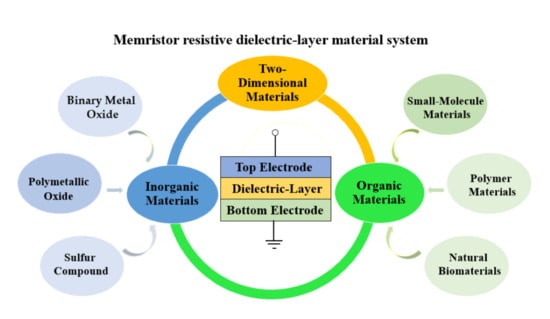
However, as an emerging research field, memristors still have key unresolved issues in terms of micro mechanisms, device reliability, and other aspects, greatly limiting their large-scale industrialization [45,46,47]. Foremost among these challenges is the pivotal issue of resistive-switching layer material selection. The choice of materials for the resistive-switching layer critically influences the realization of memristive functionalities. Typically, inorganic materials have stable performance and compatibility with CMOS. Organic materials are easy to prepare and can be used in flexible wearable devices [48]. Consequently, comprehensive investigations into memristor material systems remain imperative. Although the phenomenon of resistive change has been reported in various material systems, including metal oxide materials, sulfide materials, organic materials, and two-dimensional materials, there is currently no unified consensus on which resistive change material has more advantages. Addressing these challenges, this review systematically elucidates the impacts and advantages of various memristor resistive layer materials on device performance, providing a comprehensive overview of memristor structures employing diverse resistive layer materials.
2. Memristor
2.1. Concept and Characteristics
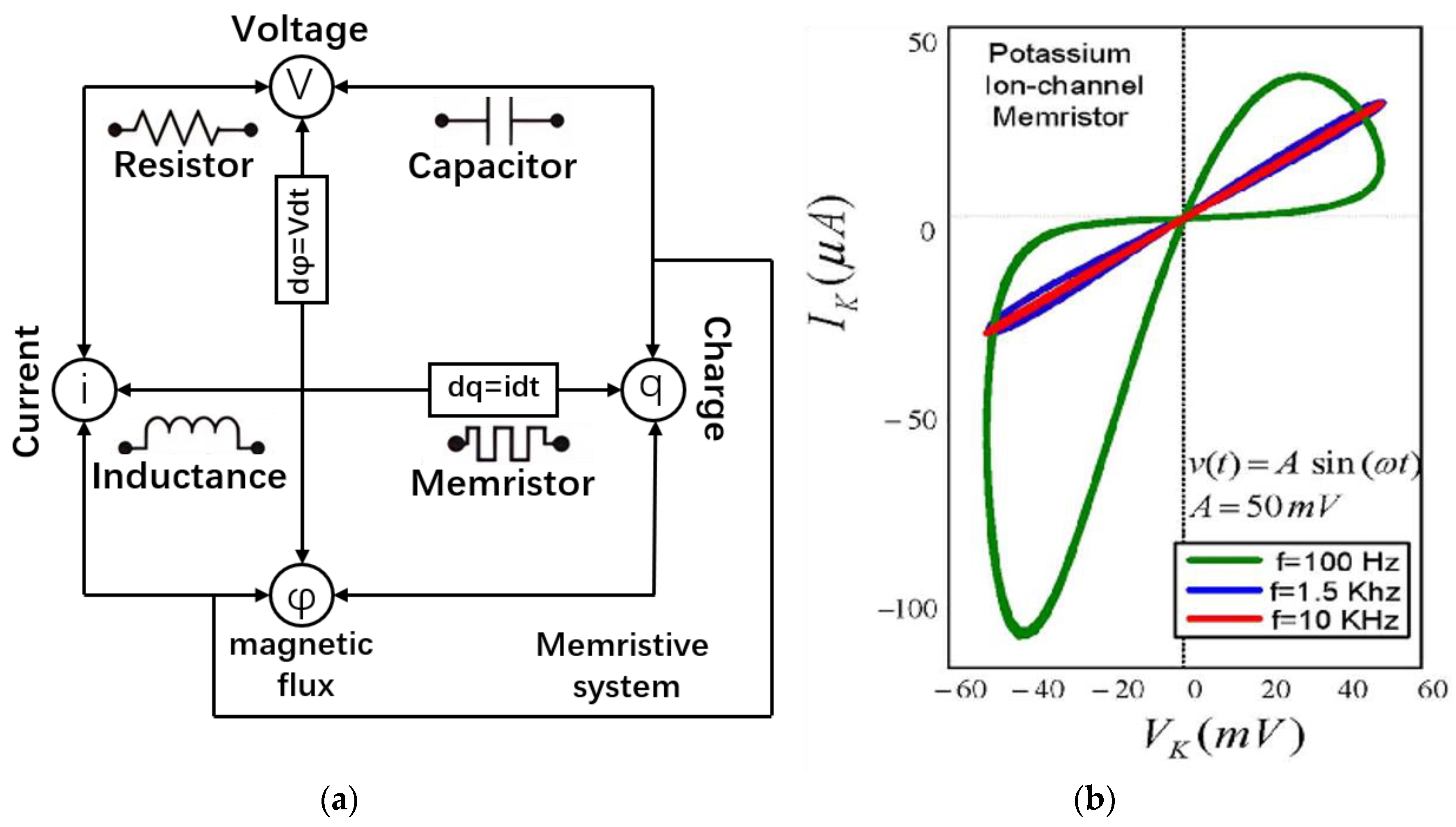
In 1971, Professor Leon O. Chua first introduced the concept and theoretical model of the memristor. It is recognized as the fourth-largest basic passive-circuit component alongside resistors, capacitors, and inductors [49]; the memristor’s relationship with these basic circuit elements is depicted in Figure 1a. Fundamentally, the memristor operates as a nonlinear element, exhibiting variations in its resistance value based on the historical input current or voltage. This characteristic enables it to “remember” the charge or magnetic flux that has passed through it [50,51].
In 2008, HP Labs pioneered the fabrication of a Pt/TiO2/Pt device; it displayed a hysteresis loop under a voltage sweep, aligning with the memristive characteristic curve proposed by Professor Leon O. Chua [24]. This seminal work from HP Labs bridged the previously recognized resistance-switching phenomenon with memristor theory, transitioning the concept of memristors into tangible devices. Subsequent investigations have unveiled memristive behaviors in various materials and devices, including binary oxides, perovskite-type oxides, and organic materials, leading to the fabrication of an increasingly diverse array of memristive devices [53,54,55].
In 2011, Professor Chua L. proposed that regardless of the type of resistive material or physical mechanism, any two terminal devices that can exhibit the characteristic of a hysteresis loop is a memristor [56], as depicted in Figure 1b. He subsequently delineated three foundational criteria for identifying memristors [52]: (1) Under bipolar periodic signal stimulation, the device exhibits a “hysteresis loop” in the current–voltage plane. (2) From a critical frequency onwards, the area of the hysteresis loop should diminish as the excitation frequency increases. (3) At sufficiently high frequencies, the hysteresis loop contracts to a single-valued function.
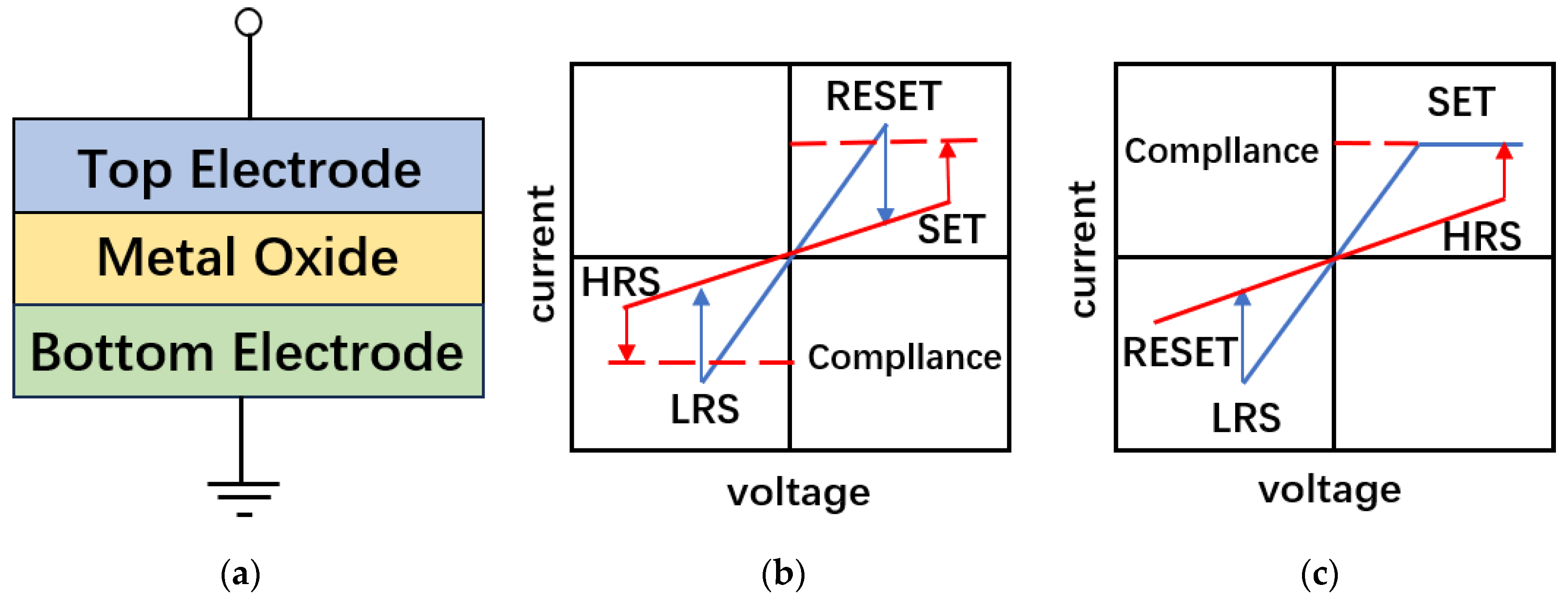
Conventional resistive random-access memory (RRAM) serves as a quintessential two-terminal device, characterized by a straightforward “sandwich” configuration of top electrode-insulator-bottom electrode (MIM), as depicted in Figure 2a. Under the influence of external electrical stimuli, the RRAM undergoes a resistive transition. Upon removal of the excitation signal, the RRAM retains its resistance state, exhibiting non-volatile characteristics. This non-volatility, derived from distinct resistive states, facilitates information storage within the device [57]. Based on the current–voltage characteristic curves, the resistive-switching modes of RRAM can be categorized into unipolar and bipolar resistive-switching, as illustrated in Figure 2b,c. For unipolar devices, the transition between high-resistance state (HRS) and low-resistance state (LRS) is independent of the polarity of the applied electrical signal, contingent solely upon the magnitude of the applied voltage. Consequently, the device can be subjected to both SET and RESET operations by applying voltages of similar polarity but varying magnitudes. Conversely, in bipolar devices, the transition between HRS and LRS is contingent upon both the polarity and magnitude of the applied electrical signal. Therefore, the voltage polarity is opposite during the SET and RESET processes. Devices can only achieve the SET process under electrical signals of a certain polarity, and they generally require the application of limited current protection during the resistance change process and electrical preprocessing process. This can avoid hard breakdown of the device due to excessive current during the SET process, causing permanent failure of the device. The RESET process can be achieved under opposite polarity voltage signals [58].
The different characteristics of memristors determine their applications in different fields. When used as a memory, it is necessary to have a wide resistance window, and the ratio between the HRS and LRS of the memristor is required to be as large as possible. In terms of synaptic applications, the memristor is a continuous control of resistance through continuous application of positive and negative operating voltages, which can realize the plasticity and memory of the memristor, so as to realize the function of learning and memory similar to synapses. The better the intermediate resistance control and the closer the performance to biological synapses, the better the neurosynaptic simulation. At the same time, the retention time of the memristor and the thermal failure at high temperature reflect the retention and stability of the memristor. The difference of each parameter leads to the application of memristors in different fields, in which the selection of resistive dielectric layer materials is the key to achieving memristor performance. The memristor performances achieved by different dielectric layer materials are different, as shown in Table 1.
It is worth noting that the process of realizing the memristor characteristics not only depends on the dielectric layer material used but also on the material used as the electrode, and the performance of the memristor will also change when the electrode is replaced. For example, Shen [64] found in his study on the performance changes of solution-treatment memristors induced by different top electrodes that AlOx layers were prepared in increments of 50 °C at different annealing temperatures of 225–275 °C. Both Ni/AlOx/Pt and TiN/AlOx/Pt RRAM devices exhibit bipolar RS performances. Compared with TiN electrode materials, RRAM devices using Ni electrode materials show better characteristics at all temperatures, lower operating voltage, and better stability.
2.2. Resistive Mechanism of Memristor
2.2.1. Interface Barrier Mechanism
Under the influence of an electric field, electron/oxygen vacancies aggregate or migrate at the interface, causing a change in the width of the Schottky barrier or depletion layer at the interface. The mechanism that causes high and low changes in the resistance value of the device is called the interface barrier mechanism [65,66,67]. Schottky barrier types are categorized based on their contact with P-type or N-type semiconductors. At a P-type interface, when the electric field causes oxygen vacancies to accumulate at the interface, the barrier height increases, resulting in a high-resistance state for the device. Conversely, when oxygen vacancies depart from the interface, the barrier height diminishes, leading to a low-resistance state. Figure 3a,b illustrates the modulation mechanism of the Schottky barrier at a P-type interface in its high and low-resistance states. In contrast, for an N-type interface, the resistance decreases with an increase in oxygen vacancies, exhibiting the opposite characteristics to that of a P-type interface.
2.2.2. Metal Conductive Wire Mechanism
Under the influence of an electric field, the metallic top electrode undergoes oxidation-reduction reactions, leading to the deposition or dissolution of metal between the top and bottom electrodes. This process controls the formation or melting of conductive filaments, known as the metallic filamentary conduction mechanism. The underlying principles of this mechanism are as follows: (1) Under positive voltage, the anodic metal undergoes oxidation, losing electrons and transforming into metal ions. (2) These metal ions migrate towards the cathode through the dielectric medium. (3) Upon reaching the cathode, the metal ions undergo reduction reactions. As the accumulated metal continues to reach the anode, conductive filaments form. In TEM observations in the Ag/SiO2/Pt system, as depicted in Figure 4, silver conductive filaments are discerned. At this time, the device transitions from a high-resistance state to a low-resistance state. Conversely, upon application of a reverse voltage, the conductive filaments dissolve, causing the device to revert from a low-resistance to a high-resistance state [69,70,71].
2.2.3. Oxygen Vacancy Conductive Wire Mechanism
Under the influence of an electric field, oxygen ions undergo migration, leading to changes in the oxidation states of the oxide material. Within the device, this results in the formation of conductive filaments composed of oxygen vacancies, a resistive-switching mechanism known as the oxygen vacancy filamentary conduction mechanism [73,74,75,76]. When a positive voltage is applied, oxygen ions migrate towards the anode, leaving immobile oxygen vacancies within the dielectric layer. As these vacancies accumulate, conductive filaments form, causing the device to transition from a high-resistance state to a low-resistance state. Conversely, upon application of a reverse voltage, oxygen ions recombine within the dielectric layer, depleting the oxygen vacancies. Therefore, the conductive filaments rupture, causing the device to revert from a low-resistance state to a high-resistance state. Figure 5 illustrates the resistive-switching phenomenon in a Pt/ZnO/Pt system based on the oxygen vacancy filamentary conduction mechanism [77].
3. Selection of Dielectric Layer Material for Memristor
Since the proposal of the memristor model based on TiO2 by HP Labs, an increasing array of novel materials have been employed in the construction of memristor models. The selection of memristor materials is an extremely important step in constructing a memristor model, and its material system includes dielectric layer materials and electrode materials. The dielectric layer materials mainly include inorganic materials, organic materials, and two-dimensional materials. In this study, inorganic materials are further classified into multicomponent metal oxides, binary metal oxides, and sulfur-based compounds. Organic materials are divided into small molecule materials, polymer materials, and biomaterials. Subsequently, the research progress of various memristor dielectric layer materials is emphasized, along with an exploration of the advantages and limitations associated with each category of memristor dielectric materials.
3.1. Memristors Based on Inorganic Materials
Traditional inorganic memristor devices, compared to those fabricated from organic materials, have a longer history of development. Typically, memristors based on inorganic materials are characterized by stable performance and a well-understood mechanism. Currently, research on inorganic memristors predominantly focuses on materials such as metal oxides and sulfur-based compounds. This section provides a comprehensive overview of the development trajectory of these specific inorganic materials, detailing their advantages, disadvantages, and strategies for enhancement.
3.1.1. Binary Metal Oxide
Binary metal oxide materials have many advantages, such as simple structure, diverse types of oxides, fewer impurities and defects, easy control of composition ratios, and strong compatibility between the preparation process and existing CMOS processes. Various binary metal oxides, such as TaOx [78], TiOx [79], NiO [80], AlOx [81], and HfOx [57], have been extensively researched due to the discovery of resistive-switching characteristics in these materials. This section focuses on the research progress of HfOx-based memristors.
Hafnium oxide (HfO2) is a conventional high-k dielectric material [82]. When it possesses a high concentration of defects, it exhibits excellent resistive-switching properties. Memristors based on HfO2 showcase attributes like a large ON/OFF ratio, high endurance, retention, multi-bit storage capabilities, and rapid operation [83,84,85,86,87]. In 2007, Lee fabricated memristors based on HfOx thin films using atomic layer deposition (ALD) and observed resistive-switching phenomena [88]. Specifically, when x = 1.5 in the Pt/HfOx/TiN/Si memristor structure, it demonstrated reversible unipolar resistive switching with an ON/OFF ratio exceeding 100. Furthermore, with its good data-retention ability, it is expected to be applied to high-density memory. However, challenges related to consistency and stability remain in HfOx memristors.
Subsequently, an increasing number of different media were proposed for application in the stack of RRAM memory. Azzaz introduced a 1 nm Al2O3 layer at the HfO2 interface, serving as a tunneling layer between the top and bottom TiN electrodes [84], as shown in Figure 6a. Compared to single-layer HfOx devices, the HfOx/AlOx bilayer RRAM showcased improved uniformity in switching voltages and reduced HRS resistance dispersion. A thin Al2O3 layer can improve durability and data retention (both low and high-resistance states remain stable after 6 h at 200 °C). The data retention of the memristor was tested as shown in Figure 6b, and it was found that this structure effectively improves the device erase consistency and resistance state retention time of the memristor. Among other elements, rare earth elements are abundant in content. After incorporating it into the memristor, the formation energy of oxygen vacancies around the rare earth decreases, and the random distribution of oxygen vacancies is suppressed. This can greatly improve the parameter discreteness, durability, and data retention of memristors. Dong [59] studied the electrical properties of HfOx memristors doped with La, Ce, and Gd. Memristors were fabricated with a Ta/La (Ce, Gd): HfOx/Au/Cr/SiO2/Si structure. Comparative analysis revealed that doping did not alter the resistive-switching mechanism. After doping, the SET voltage and RESET voltage of the memristor decrease, and the increase in high-resistance state resistance leads to an increase in its storage window. The durability and data-retention characteristics of the memristor structure are greatly improved.
The demand for high-voltage electroforming hinders the commercialization of RRAM technology, and research on electroforming-free memristors is particularly necessary when considering low-voltage sources for more advanced CMOS technology nodes. In 2024, Mari Napar [89] prepared single-layer and double-layer resistive-switch storage devices of tantalum oxide (TaOx) and hafnium oxide (HfOx) using the atomic layer deposition method, as shown in Figure 6c. This device has nonlinear switching characteristics and can operate without the need for initial electroforming steps. Inserting thin (3 nm) HfOx into the TE/TaOx/TiN diode stack can induce resistance-switching behavior. Double-layer devices do not require a formation process to activate switching characteristics, and they exhibit bipolar switching modes, where positive bias and negative bias turn on (set) and off (reset) the device, respectively.
Binary metal oxides also possess certain limitations. For instance, a majority of these metal oxides exhibit biocompatibility issues and a lack of stretchability, which significantly hinders their application in flexible and stretchable devices as well as in large-area integrated circuits.
3.1.2. Polymetallic Oxide
Polymetallic oxide is an oxide material composed of many metals, and it is also the first-studied resistive material. At present, the multi-metal oxides that have been applied to memristors include ternary oxides LiCoO2, SrZrO3, SrRuO3, etc; quaternary oxides (LaSr) MnO3, La0.33Sr0.67FeO3, Pr0.7Ca0.3MnO3, etc; and five-membered metal oxides PryLa0.625−yCa0.375MnO3, etc.
During the initial phases of RRAM development, polymetallic oxides were incorporated into the research scope of resistive materials. Among these, lithium ions (Li+) have been extensively utilized in RRAM research due to their outstanding electrochemical properties. Mai [90] observed memory behavior in LiCoO2 thin films and demonstrated significant bipolar resistive-switching (RS) phenomena in Au/LixCoO2/doped-Si devices. The ratio of Roff (highest resistance) to Ron (lowest resistance) is between 104–105, indicating a stable resistance state. Notably, the conductivity of LiCoO2-based RRAM is influenced by the concentration of Li ions. When the bottom Si electrode is negatively polarized, Li ions migrate to the doped Si electrode. They are reduced by forming LixSi complexes, generating electromotive force, and forming conductive filaments. SiO2 grows through thermal oxidation before the deposition of LixCoO2. After the deposition of LixCoO2 film on Si, a natural SiO2 layer with a thickness of 2–3 nm is formed at the LixCoO2/Si interface. SiO2 allows Li ion diffusion and prevents short circuits between electrodes, but the SiO2 layer formed by this memristor is considered too thin to avoid short circuits. To investigate the influence of SiO2 on the resistive behavior of LiCoO2-based RRAM, Hu [91] introduced SiO2 as a buffer layer in the RRAM and fabricated Pt/LiCoO2/SiO2/Si multilayers with varying SiO2 thicknesses. Their experiments revealed that the RRAM I–V curves became smoother with the introduction of the SiO2 layer, and the resistive-switching phenomenon became more pronounced. Furthermore, due to the difference in material thickness, the performance of the memristor will also be affected. Hu conducted durability tests on LiCoO2 memristors with different thicknesses of SiO2 layers, and ultimately found that the Vset and Vreset of the SiO2 layer with a thickness of 20 nm were more stable.
In the same year, Gao [60] optimized the aforementioned RRAM structures by proposing a layered porous (KLHP) silicon oxide (PSiOx) structure similar to karst topography. Their devised structure was Au/LixCoO2/PSiOx/Si. The porosities within SiO2 facilitated rapid ion transport and ensured ample contact between lithium ions and the silicon oxide. The interconnected porous structures of varying sizes significantly reduced lithium ion diffusion barriers, imparting enhanced stability and repeatability to the RRAMs. As illustrated in Figure 7a,b, endurance tests on Pt/LiCoO2/SiO2/Si and Au/LixCoO2/PSiOx/Si RRAMs in HRS and LRS states clearly indicate that the layered porous silicon oxide RRAM system exhibits superior stability in both high and low-resistance states. Additionally, its multi-layered porous structure renders it highly valuable for simulating neural network computations.
While polymetallic oxide-based RRAM devices exhibit favorable resistive-switching characteristics, their complex compositional makeup and the challenges in precisely controlling the resulting crystal shapes pose significant hurdles. Moreover, their compatibility with CMOS technologies is limited. These factors collectively restrict their applicability in the domain of resistive memories.
3.1.3. Sulfur Compound
Apart from polymetallic oxides, chalcogenide compounds serve as a class of solid-state electrolyte materials, characterized by their rich functional defect properties that facilitate ion transport. The resistance-variation mechanism based on chalcogenide compounds is usually achieved by the switching of metal conductive filaments between high and low resistance states of the thin film. Commonly employed chalcogenide compounds include Cu2S [92], GeSbTe [93], and Ag5In5Sb60 [94].
In 2014, Zhang [95] investigated the performance of Te-based chalcogenide RRAMs, specifically Ge2Sb2Te5, Sb2Te3, and Ag5In5Sb60. By varying the electrode materials (Tiw, Ag, Ta, and ITO), it was observed that Ge2Sb2Te5 RRAMs with Ag electrodes exhibited the most favorable switching characteristics. The ratio between high and low resistance exceeds 50, and it has good repeatability. These devices are well-suited for non-volatile memory and logic operations in digital applications. Meanwhile, the Ag5In5Sb60 compound, which contains Ag, demonstrates pronounced intrinsic defects in its amorphous state. This has led to RRAMs with superior resistance-modulation characteristics. Specifically, by controlling the current, distinct post-positive-voltage-sweep resistive states were achieved. These devices showed consistent resistive-switching properties and hold promise for multi-level storage and analog applications, such as emulating synaptic functions in neural networks. Among the Te-based chalcogenides, Sb2Te3 stands out as a frequently studied compound. RRAMs based on Sb2Te3 display stable switching characteristics and efficient resistance modulation. The speed of resistance modulation in Sb2Te3 RRAMs exceeds that of Ag5In5Sb60 devices. However, there remains room for improvement in terms of the resistance ratio and the consistency of resistance modulation.
In recent years, doping strategies have been adopted to enhance the performance of chalcogenide materials. For instance, in the undoped amorphous GeTe, two structural configurations exist: tetrahedral and defect octahedral structures. While the tetrahedral structure imparts strong amorphous stability to GeTe, making it resistant to crystallization, the defect octahedral structure promotes crystallization. By introducing elements like Cu and Ag, the octahedral structures in GeTe tend to transform into tetrahedral ones, enhancing its amorphous stability [96]. Research by Chen Jianwen [61] focused on Ag-doped AgGeTe (AGT) and AgInSbTe (AIST) materials. I–V curve measurements revealed that AGT-based RRAMs exhibit a broad storage window with a resistance ratio reaching 254. These devices showcased excellent multi-level properties, maintaining stability over time, indicating that the observed resistive states were not random but could be modulated by current constraints. In contrast, AIST-based RRAMs also demonstrated stable multi-level characteristics with a lower operating voltage range (−0.5 V to 0.5 V), resulting in reduced power consumption. However, they exhibited a narrower resistance window with a resistance ratio of only 35 and displayed significant temperature susceptibility, showing thermal degradation beyond 110 °C.
Despite significant advancements in the study of resistive-switching properties of chalcogenide compounds in recent years, several critical challenges persist. The resistive-switching mechanisms of certain chalcogenide materials remain inadequately elucidated. Additionally, their resistive-switching characteristics are predominantly confined to conventional I–V behaviors, lacking broader applicability across various domains. Moreover, comprehensive investigations into their thermal properties are still lacking. These limitations pose obstacles to the practical application of chalcogenide-based resistive-switching devices.
3.2. Memristors Based on Organic Materials
Organic materials offer a diverse array of synthesis methods [97], enriched with a plethora of functional groups. Additionally, they possess notable attributes such as mechanical flexibility, high ductility, and lightweight nature [98,99,100,101]. As early as 1979, metal organic complex thin-film M-TCNQ was reported to have excellent electrical bi-stability. Resistive-switching devices based on organic materials have been recognized for their exceptional flexibility, tunable performance, and adaptability [102,103]. Consequently, organic materials have emerged as pivotal constituents within the resistive-switching material framework; these are further categorized into three major classes: small organic molecules, polymers, and bio-materials.
3.2.1. Organic Small-Molecule Materials
Owing to their well-defined structures, ease of purification, and cost-effectiveness, organic small molecules have garnered significant attention in the realm of organic materials. Wang [104] developed a resistive-switching device structured as ITO/CuPc/Al using the organic small molecule CuPc. This device leverages polycrystalline CuPc domains as charge reservoirs, endowed with numerous current-blocking traps. This configuration facilitates enhanced and suppressed tendencies during reversible charge capture and release, resulting in a gradual transition and quasi-continuous characteristics of the conductive state. The experimental results show that the device has a memristor response, and the I–V characteristic curve based on the CuPc memristor has a gradual smoothing feature. With the rapid development of flexible electronic technology in recent years, the demand for flexible memory is becoming increasingly high, requiring smaller information storage points and higher-density storage units to meet the data-storage requirements in flexible electronic products. The compatibility of organic materials with flexible substrates and their scalability makes them pivotal for ultra-high-density information storage in flexible resistive memories. Li Tengfei [105] prepared an organic diode memristor based on ZnTPP, which precisely regulated the carrier transport through the formation and fracture of the coordination bond formed by the central metal zinc ion and oxygen ion, thus achieving a stable, smooth, and gradual resistive behavior. By realizing the basic memristor function, the synaptic properties of ZnTPP memristors under different bending times and bending radii were studied, showcasing their powerful and flexible synaptic device capabilities and the possibility of designing flexible memristors using organic materials. Subsequently, in the study of flexible memristors, Liu Lutao [106] prepared an organic flexible TPP memristor with a device structure of PET-ITO/TPP/Al2O3–x/Al based on PET–ITO conductive film. It was found that after bending the organic flexible TPP memristor 50 and 100 times, the memristor curve would gradually become rough with the increase in bending, though it still showed good stability and synaptic plasticity. Even so, the lack of stability of small organic molecules at higher temperatures is still an issue that cannot be ignored. For this reason, Yi Mingdong’s [107] research group successfully developed a stable memristor in a high-temperature air environment by using copper monochloro-phthalocyanine as the functional layer of the organic memristor. The molecular structure diagram of ClCuPc is shown on the left side of Figure 8a. On the right is the ITO/ClCuPc/Al memristor device structure. By studying the changes of microstructure and the molecular structure of dielectric films before and after high temperature, it was found that the introduction of chlorine atoms can effectively improve the thermal stability and air stability. The device can operate at temperatures up to 300 °C in an air environment without any packaging and perform normal resistance switching after annealing at 400 °C, simultaneously maintaining a stable memristive performance in the air environment for 314 days. Figure 8b shows the enhancement of continuous positive stimulus triggering for 100 s at different temperatures (250 °C, 275 °C, and 300 °C). The corresponding flexible device was also prepared on a flexible substrate. After 100 repetitions of mechanical bending, the device still maintained good memristor performance. As shown in Figure 8c, effective flexible expansion capability is demonstrated.
3.2.2. Polymer Materials
Polymers have good solubility, stability, film-forming ability, and mechanical strength in organic solvents. Their advantages, such as low production cost and compatibility with CMOS technology, have been widely studied by researchers. In 2011, Bandyopadhyay pioneered a polymer-based resistive switch by employing solution methods to create cobalt (III) with both conjugated and non-conjugated polymer and azo-aromatic frameworks. They observed bipolar switching between high and low resistive states in the I–V curve, as well as hysteresis differences between the conjugated and non-conjugated groups. Subsequently, Li [108] proposed a resistive switch structured as Ag/PEDOT:PSS/Ta. Analysis of the cross-sectional transmission electron microscopy (TEM) images of the memory device confirmed that the resistance state alteration was attributed to the movement of silver at the interface and ensuing redox reactions, as illustrated in Figure 9a,b. Similarity to human learning and memory functions was observed when simulating the basic plasticity behavior of synapses using this memristor. This indicates that the memristor can meet the basic requirements of neural morphology calculations. Furthermore, a natural p–n junction formed between PEDOT:PSS and Ta compounds, rectifying the memory device and endowing the resistive switch with characteristics such as high resistance and low power consumption.
In subsequent research on polymer materials, researchers found that due to the high crystallinity and low ion-conductivity of polymers, metal cations can only move a short distance near the interface through electrode injection, thereby reducing the dynamic adjustment range of resistive states in memristive devices. Addressing this, Liu [109] fabricated a resistive switch based on [EV(ClO4)2] + PEO/BTPA-F, as depicted in Figure 9c. The observed electrical transitions indicate that the tuning of the device’s conductivity is smoother during the voltage scanning process. Furthermore, each subsequent scan of the I–V circuit picks up areas where the last scan was interrupted or partially overlapped, exhibiting typical memristive characteristics. The principle lies in the BTPA-F copolymer possessing a closed-ring and densely packed TPA group. When a positive electric field is applied, the unshared electron pairs on the nitrogen atoms of the TPA segment vanish, oxidizing the polymer and introducing impurity energy levels into the material’s bandgap, as illustrated in Figure 9d. Consequently, the conductivity of the BTPA-F polymer and device is significantly enhanced through intra-chain and inter-chain hopping of these charged centers. Then, the simulation of biological synapses is achieved by increasing the frequency of applied voltage pulses, gradually increasing the frequency from 1 Hz to 20 Hz. The higher the frequency of synaptic stimulation, the higher the current, as shown in Figure 9e. This also proves that the synaptic plasticity behavior achieved by the device meets the basic requirements of neural morphology calculations.
The structural anisotropy and non-uniformity of most polymer materials result in uneven distributions of electric fields in the prepared thin films, leading to low device yield and reliability. To address this issue, Chen [62] designed a two-dimensional conjugated polymer, PBDTT-BQTPA. Research has shown that the ordered π–π stacking of coplanar thiophene quinoline D–A pairs and macromolecular frameworks enhances the crystal uniformity of polymer films. As shown in Figure 10a,b. Uniform resistance switching has been achieved throughout the entire organic layer, with switch parameter changes reduced to 3.16–8.29% and production approaching 90%. Resistive devices based on PBDTT-BQTPA were capable of universal memory Boolean logic, arithmetic operations, and binary neural networks. However, for devices to be widely utilized in neural network computations, achieving a large dynamic range modulation of pulse conductance is indispensable. To address this, Wang [110] incorporated ammonium nitrate and polyvinyl alcohol into carboxymethyl chitosan, fabricating a resistive switch based on carboxymethyl chitosan-ammonium nitrate-polyvinyl alcohol (PVA). This device significantly increased ion conductivity, widening the ion transport channels and facilitating metal-ion migration and redox reactions, thereby reducing operating voltages. Additionally, the introduction of polyvinyl alcohol substantially enhanced device retention. In addition, the device also exhibited good performance in regulating the conductivity state under pulse testing. Under low voltage, it can be cycled 10 times, and under continuous voltage stimulation of 3 V, it can achieve a dynamic amplitude adjustment of conductivity of more than one order of magnitude. It demonstrates excellent non-volatility and synaptic plasticity, making it a favorable candidate for future artificial neural synaptic nanodevices.
3.2.3. Natural Biomaterials
Due to their flexibility, biocompatibility, and sustainability, natural biomaterials have garnered significant interest from researchers. Starch, lignin, proteins, glucose, enzymes, DNA, citric acid, silk fibroin, nanocellulose, and more have been employed in organic resistive memory studies. This section focuses on resistive devices based on silk fibroin.
Silk fibroin (SF) is a biomass material with good biocompatibility, adjustable degradation performance, and easy processing. Furthermore, it has been proven to have memristive functions, showing good comprehensive performance in constructing memristors. In 2017, Liu [111] introduced gold nanoclusters (AuNCs) into SF, fabricating a AuNCs-SF composite resistive layer. Compared to pure SF devices, it exhibited improved stability, repeatability, and significantly lower threshold voltages of 0.4 V and −0.3 V, implying reduced power consumption. The resistance ratio between HRS and LRS was substantially larger than pure SF-based devices, minimizing read errors and facilitating peripheral circuit storage applications. After extensive SF research, it was discovered that through modification or compositing with other materials, multi-resistive state transitions within a single voltage cycle and multi-level storage under different Icc could be achieved. In terms of multi-stage storage resistive device research, in 2022, Zhu [112] prepared high-performance volatile memristors based on silver nitrate (AgNO3)-doped SF. This memristive device had good device uniformity, reliable repeatability (>100 cycle times), and a low threshold voltage of 0.17 V. Meanwhile, the SF-based memristive device also had good environmental stability and could maintain relatively stable memristive functions even at 80 RH% humidity and 70 °C. Moreover, by setting five different Icc, five different low-resistance states (LRS) could be obtained, thereby achieving multi-level storage functions.
Sericin, as a bioactive and biocompatible biomaterial, has also been applied in the research into memristors. In 2023, Nan He [113] designed an artificial neuron application memristor with a Ag/AIZS/sericon/W structure. Through systematic electrical analysis, it was demonstrated that the manufactured sericin-based device exhibited reliable behavior through more than 100 DC continuous cycles, a low and concentrated operating voltage, and excellent cycle and inter-device uniformity. In addition, basic neuronal functions were demonstrated using a single sericin-based device, as shown in Figure 11a,b. A MNIST handwritten-digit-recognition SNN with a recognition rate of up to 91.44% was established based on the neural characteristics of sericin devices, providing a feasible approach for constructing advanced SNNs using high-performance artificial neurons.
3.3. Memristors Based on Two-Dimensional Materials
The low-dimensional structure of two-dimensional materials leads to their unique electronic properties, giving them enormous potential in the fields of electronic devices and energy. Compared to traditional three-dimensional materials, they have a larger specific surface area and stronger adsorption and catalytic performances, providing a larger reactive surface for various applications. Despite their thin thickness, they still exhibit excellent mechanical properties.
In the exploration of two-dimensional materials, Zhang [114] proposed a MHM memristor architecture based on a WS2/MoS2 dielectric layer. Compared with traditional two-dimensional-material-based MIM memristors, MHM-based two-dimensional memristors can eliminate the serious structural damage caused by filament formation/fusing during the set/reset process, greatly improving the stability of memristors. The device can achieve a switching ratio of 104 and maintain more than 120 set/reset cycles under a stable memory window, as shown in Figure 12a,b. However, due to limitations in manufacturing technology during the synthesis process of two-dimensional materials, the device can still be improved.
Among other two-dimensional materials, graphene oxide (GO) has been widely studied by researchers due to its excellent conductivity, thermal conductivity, good mechanical strength, and flexibility. Liu [63] constructed an ITO/GO/SF/GO/Al composite memristor by combining graphene oxide (GO) with SF. This memristor had a good continuous resistance adjustability and could integrate single-cycle triple-resistance state transitions and double-resistance state transitions by adjusting the Icc. When testing the device’s triple-resistance state time-retention characteristics, it was found that all resistance states could be stably maintained for 104 s. Furthermore, this type of memristor structure could stably cycle more than 50 times in both transition modes, store stably for 30 days, and simulate behaviors such as synaptic plasticity. In 2023, Xie [115] further conducted research on synaptic memristors and prepared a Pt/BiOI/Pt memristor, which exhibited typical bipolar RS behavior. The adjustable resistance state could be used to simulate the “learning-forgetting” experience of the human brain, as shown in Figure 12c. Furthermore, the synaptic memristor could achieve repeatable long-term enhancement (LTP) and long-term inhibition (LTD) cycles, which could be used to simulate image recognition of artificial neural networks with an accuracy rate of up to 91.15%. There is enormous potential in neuromorphic computing.
However, two-dimensional materials also have some drawbacks, such as the relatively complex preparation process of certain two-dimensional materials, which requires high-precision control and preparation techniques. Moreover, due to their surface activity and low-dimensional properties, some two-dimensional materials are more sensitive to humidity, oxidation, and chemical environments, resulting in relatively poor stability.
4. Conclusions
As a novel memory storage technology, resistive random-access memory (RRAM) achieves data storage via impedance changes. Due to its capability to meet the demands for high efficiency, low power consumption, and high density, RRAM presents vast application prospects for the future. This article first briefly describes the basic concept, structure, and resistance-variation mechanism of memristors. Secondly, the materials of the dielectric layer are divided into three categories: inorganic materials, organic materials, and two-dimensional materials. The impact of different categories and resistance variation materials on the performance of memristors is described in detail.
From the analysis of these RRAM dielectric layer materials, several observations emerge:
(1) Metal-oxide-based RRAM devices have good resistance characteristics, a large resistance window, easy control of component ratios, and strong compatibility with existing CMOS processes in their preparation process. They are commonly used as memory devices.
(2) Sulfur-based compound materials have rich functional layer defects, which are very conducive to ion transport and have significant advantages in preparing high-speed and multi-value storage memristors.
(3) Organic materials have diverse synthesis methods and rich functional groups. Organic small molecules play a significant role in the research of flexible memristors due to their clear structure, easy purification, and low cost. Polymer materials have good solubility, stability, film-forming ability, and mechanical strength in organic solvents, and they are often used in neural network calculations due to their low production cost and compatibility with CMOS technology.
(4) Two-dimensional materials have excellent physical and electrical properties and can be applied in large-area flexible devices; they are also commonly used as neural synaptic devices.
Despite its rapid progression, RRAM technology grapples with several challenges. Foremost among these is device consistency: deviations in set voltage across different devices can lead to operational errors or even circuit malfunctions. This issue becomes even more critical in precision-computing applications where stringent device consistency is paramount. Additionally, device stability remains a concern. Although significant strides have been made in enhancing device stability through diverse materials and methodologies in RRAM research, these factors still hinder its large-scale industrialization. Consequently, future endeavors should focus on identifying alternative resistance-switching materials or refining existing techniques to bolster RRAM consistency and stability, paving the way for its widespread integration into everyday applications.
Author Contributions
Conceptualization and funding acquisition, C.W.; writing original draft preparation, X.L.; investigation, Z.S.; writing-review and editing, Y.L. and L.C.; visualization, Y.Y. All authors have read and agreed to the published version of the manuscript.
Funding
This work was funded by the Natural Science Foundation of Chongqing (Grant Nos. cstc2021jcyj-msxmX0576, CSTB2023NSCQ-MSX0425), the Scientific and Technological Research Program of Chongqing Municipal Education Commission (Grant Nos. KJQN202200518, KJQN202200545, KJQN202300548, and KJZD-K202300516), and the Curriculum ldeological and Political” Demonstration Project of Chongqing Municipal Education Commission (No. YKCSZ23102).
Data Availability Statement
No new data were created or analyzed in this study. Data sharing is not applicable to this article.
Conflicts of Interest
The authors declare no conflicts of interest.
References
- Zidan, M.A.; Strachan, J.P.; Lu, W.D. The future of electronics based on memristive systems. Nat. Electron. 2018, 1, 22–29. [Google Scholar] [CrossRef]
- Yao, P.; Wu, H.; Gao, B.; Tang, J.; Zhang, Q.; Zhang, W.; Yang, J.J.; Qian, H. Fully hardware-implemented memristor convolutional neural network. Nature 2020, 57, 641–646. [Google Scholar] [CrossRef]
- Waldrop, M. Neuroelectronics: Smart connections. Nature 2013, 50, 22–24. [Google Scholar] [CrossRef] [PubMed]
- Muthuswamy, B.; Chua, L.O. Simplest chaotic circuit. Int. J. Bifurc. Chaos 2010, 20, 1567–1580. [Google Scholar] [CrossRef]
- Migliato Marega, G.; Zhao, Y.; Avsar, A.; Wang, Z.; Tripathi, M.; Radenovic, A.; Kis, A. Logic-in-memory based on an atomically thin semiconductor. Nature 2020, 58, 72–77. [Google Scholar] [CrossRef] [PubMed]
- Yang, J.Q.; Wang, R.; Ren, Y.; Mao, J.Y.; Wang, Z.P.; Zhou, Y.; Han, S.T. Neuromorphic engineering: From biological to spike-based hardware nervous systems. Adv. Mater. 2020, 32, 2003610. [Google Scholar] [CrossRef] [PubMed]
- Borkar, S.; Chien, A.A. The future of microprocessors. Commun. ACM 2011, 54, 67–77. [Google Scholar] [CrossRef]
- Kendall, J.D.; Kumar, S. The building blocks of a brain-inspired computer. Appl. Phys. Rev. 2020, 7, 011305. [Google Scholar] [CrossRef]
- Backus, J. Can programming be liberated from the von Neumann style? A functional style and its algebra of programs. Commun. ACM 1978, 21, 613–641. [Google Scholar] [CrossRef]
- Liu, C.; Yan, X.; Song, X.; Ding, S.; Zhang, D.W.; Zhou, P. A semi-floating gate memory based on van der Waals heterostructures for quasi-non-volatile applications. Nat. Nanotechnol. 2018, 13, 404–410. [Google Scholar] [CrossRef]
- Lan, S.; Wang, X.; Yu, R.; Zhou, C.; Wang, M.; Cai, X. Organic synaptic transistors based on a hybrid trapping layer for neuromorphic computing. IEEE Electron Device Lett. 2022, 43, 1255–1258. [Google Scholar] [CrossRef]
- Sun, K.; Chen, J.; Yan, X. The future of memristors: Materials engineering and neural networks. Adv. Funct. Mater. 2021, 31, 2006773. [Google Scholar] [CrossRef]
- Hasina, D.; Mandal, A.; Basu, N.; Srivastava, S.; Mitra, A.; Som, T. Realization of Short-and Long-Term Memories at Nanoscale and their Temporal Evolution in Two-Terminal Memristive Synapses. Appl. Surf. Sci. 2023, 611, 155563. [Google Scholar] [CrossRef]
- Waldrop, M.M. The chips are down for Moore’s law. Nature 2016, 530, 144. [Google Scholar] [CrossRef]
- Sanchez Esqueda, I.; Yan, X.; Rutherglen, C.; Kane, A.; Cain, T.; Marsh, P.; Liu, Q.; Galatsis, K.; Wang, H.; Zhou, C. Aligned carbon nanotube synaptic transistors for large-scale neuromorphic computing. ACS Nano 2018, 12, 7352–7361. [Google Scholar] [CrossRef]
- Zhu, J.; Yang, Y.; Jia, R.; Liang, Z.; Zhu, W.; Rehman, Z.U.; Bao, L.; Zhang, X.; Cai, Y.; Song, L. Ion gated synaptic transistors based on 2D van der Waals crystals with tunable diffusive dynamics. Adv. Mater. 2018, 30, 1800195. [Google Scholar] [CrossRef]
- Dongale, T.D.; Khot, A.C.; Takaloo, A.V.; Kim, T.G. Facile synthesis of nickel cobaltite quasi-hexagonal nanosheets for multilevel resistive switching and synaptic learning applications. NPG Asia Mater. 2021, 13, 16. [Google Scholar] [CrossRef]
- Lin, P.; Li, C.; Wang, Z.; Li, Y.; Jiang, H.; Song, W.; Rao, M.; Zhuo, Y.; Upadhyay, N.K.; Barnell, M. Three-dimensional memristor circuits as complex neural networks. Nat. Electron. 2020, 3, 225–232. [Google Scholar] [CrossRef]
- Hu, M.; Graves, C.E.; Li, C.; Li, Y.; Ge, N.; Montgomery, E.; Davila, N.; Jiang, H.; Williams, R.S.; Yang, J.J. Memristor-based analog computation and neural network classification with a dot product engine. Adv. Mater. 2018, 30, 1705914. [Google Scholar] [CrossRef]
- Andreou, A.G.; Meitzler, R.C.; Strohbehn, K.; Boahen, K.A. Analog VLSI neuromorphic image acquisition and pre-processing systems. Neural Netw. 1995, 8, 1323–1347. [Google Scholar] [CrossRef]
- Calimera, A.; Macii, E.; Poncino, M. The human brain project and neuromorphic computing. Funct. Neurol. 2013, 28, 191. [Google Scholar] [PubMed]
- Eberhardt; Duong. Thakoor Design of parallel hardware neural network systems from custom analog VLSI ’building block’chips. In Proceedings of the International 1989 Joint Conference on Neural Networks, Washington, DC, USA, 18–22 June 1989; Volume 2, pp. 183–190. [Google Scholar]
- Pershin, Y.V.; Di Ventra, M. Experimental demonstration of associative memory with memristive neural networks. Neural Netw. 2010, 23, 881–886. [Google Scholar] [CrossRef] [PubMed]
- Strukov, D.B.; Snider, G.S.; Stewart, D.R.; Williams, R.S. The missing memristor found. Nature 2008, 453, 80–83. [Google Scholar] [CrossRef]
- Di Ventra, M.; Pershin, Y.V. The parallel approach. Nat. Phys. 2013, 9, 200–202. [Google Scholar] [CrossRef]
- Wong, H.-S.P.; Salahuddin, S. Memory leads the way to better computing. Nat. Nanotechnol. 2015, 10, 191–194. [Google Scholar] [CrossRef] [PubMed]
- Yang, J.J.; Strukov, D.B.; Stewart, D.R. Memristive devices for computing. Nat. Nanotechnol. 2013, 8, 13–24. [Google Scholar] [CrossRef] [PubMed]
- Borghetti, J.; Snider, G.S.; Kuekes, P.J.; Yang, J.J.; Stewart, D.R.; Williams, R.S. ‘Memristive’switches enable ‘stateful’ logic operations via material implication. Nature 2010, 464, 873–876. [Google Scholar] [CrossRef]
- Jo, S.H.; Chang, T.; Ebong, I.; Bhadviya, B.B.; Mazumder, P.; Lu, W. Nanoscale memristor device as synapse in neuromorphic systems. Nano Lett. 2010, 10, 1297–1301. [Google Scholar] [CrossRef]
- Ielmini, D.; Nardi, F.; Balatti, S. Evidence for voltage-driven set/reset processes in bipolar switching RRAM. IEEE Trans. Electron Devices 2012, 59, 2049–2056. [Google Scholar] [CrossRef]
- Scott, J.F.; Paz de Araujo, C.A. Ferroelectric memories. Science 1989, 246, 1400–1405. [Google Scholar] [CrossRef]
- Auciello, O.; Scott, J.F.; Ramesh, R. The physics of ferroelectric memories. Phys. Today 1998, 51, 22–27. [Google Scholar] [CrossRef]
- Ielmini, D. Modeling the universal set/reset characteristics of bipolar RRAM by field-and temperature-driven filament growth. IEEE Trans. Electron Devices 2011, 58, 4309–4317. [Google Scholar] [CrossRef]
- Cooper, L.N.; Bear, M.F. The BCM theory of synapse modification at 30: Interaction of theory with experiment. Nat. Rev. Neurosci. 2012, 13, 798–810. [Google Scholar] [CrossRef]
- Bi, G.-q.; Poo, M.-m. Synaptic modifications in cultured hippocampal neurons: Dependence on spike timing, synaptic strength, and postsynaptic cell type. J. Neurosci. 1998, 18, 10464–10472. [Google Scholar] [CrossRef] [PubMed]
- Deac, A.M.; Fukushima, A.; Kubota, H.; Maehara, H.; Suzuki, Y.; Yuasa, S.; Nagamine, Y.; Tsunekawa, K.; Djayaprawira, D.D.; Watanabe, N. Bias-driven high-power microwave emission from MgO-based tunnel magnetoresistance devices. Nat. Phys. 2008, 4, 803–809. [Google Scholar] [CrossRef]
- Zhu, J.; Zhang, T.; Yang, Y.; Huang, R. A comprehensive review on emerging artificial neuromorphic devices. Appl. Phys. Rev. 2020, 7, 011312. [Google Scholar] [CrossRef]
- Moodera, J.S.; Kinder, L.R.; Wong, T.M.; Meservey, R. Large magnetoresistance at room temperature in ferromagnetic thin film tunnel junctions. Phys. Rev. Lett. 1995, 74, 3273. [Google Scholar] [CrossRef]
- Pi, C.; Ren, Y.; Chim, W. Investigation of bipolar resistive switching and the time-dependent SET process in silver sulfide/silver thin films and nanowire array structures. Nanotechnology 2010, 21, 085709. [Google Scholar] [CrossRef]
- Shi, Y.; Nguyen, L.; Oh, S.; Liu, X.; Koushan, F.; Jameson, J.R.; Kuzum, D. Neuroinspired unsupervised learning and pruning with subquantum CBRAM arrays. Nat. Commun. 2018, 9, 5312. [Google Scholar] [CrossRef]
- Xu, X.; Lv, H.; Liu, H.; Gong, T.; Wang, G.; Zhang, M.; Li, Y.; Liu, Q.; Long, S.; Liu, M. Superior retention of low-resistance state in conductive bridge random access memory with single filament formation. IEEE Electron Device Lett. 2014, 36, 129–131. [Google Scholar] [CrossRef]
- Jarvis, K.; Evans, P.; Nelson, A.; Triani, G. Comparisons of alumina barrier films deposited by thermal and plasma atomic layer deposition. Mater. Today Chem. 2019, 11, 8–15. [Google Scholar] [CrossRef]
- Jeong, D.S.; Thomas, R.; Katiyar, R.; Scott, J.; Kohlstedt, H.; Petraru, A.; Hwang, C.S. Emerging memories: Resistive switching mechanisms and current status. Rep. Prog. Phys. 2012, 75, 076502. [Google Scholar] [CrossRef]
- Kvatinsky, S.; Nacson, Y.H.; Etsion, Y.; Friedman, E.G.; Kolodny, A.; Weiser, U.C. Memristor-based multithreading. IEEE Comput. Archit. Lett. 2013, 13, 41–44. [Google Scholar] [CrossRef]
- Meuffels, P.; Soni, R. Fundamental issues and problems in the realization of memristors. arXiv 2012, arXiv:1207.7319. [Google Scholar]
- Jeong, D.S.; Kim, K.M.; Kim, S.; Choi, B.J.; Hwang, C.S. Memristors for energy-efficient new computing paradigms. Adv. Electron. Mater. 2016, 2, 1600090. [Google Scholar] [CrossRef]
- Silva, F.; Sanz, M.; Seixas, J.; Solano, E.; Omar, Y. Perceptrons from memristors. Neural Netw. 2020, 122, 273–278. [Google Scholar] [CrossRef]
- Li, Y.; Wang, Z.; Midya, R.; Xia, Q.; Yang, J.J. Review of memristor devices in neuromorphic computing: Materials sciences and device challenges. J. Phys. D Appl. Phys. 2018, 51, 503002. [Google Scholar] [CrossRef]
- Chua, L. Memristor-the missing circuit element. IEEE. Trans. Circuit Theory 1971, 18, 507–519. [Google Scholar] [CrossRef]
- Chua, L.O.; Kang, S.M. Memristive devices and systems. Proc. IEEE 1976, 64, 209–223. [Google Scholar] [CrossRef]
- Chua, L. Resistance switching memories are memristors. In Handbook of Memristor Networks; Springer: Cham, Switzerland, 2019; pp. 197–230. [Google Scholar]
- Adhikari, S.P.; Sah, M.P.; Kim, H.; Chua, L.O. Three fingerprints of memristor. IEEE Trans. Circuits Syst. I Regul. Pap. 2013, 60, 3008–3021. [Google Scholar] [CrossRef]
- Wong, H.-S.P.; Lee, H.-Y.; Yu, S.; Chen, Y.-S.; Wu, Y.; Chen, P.-S.; Lee, B.; Chen, F.T.; Tsai, M.-J. Metal–oxide RRAM. Proc. IEEE 2012, 100, 1951–1970. [Google Scholar] [CrossRef]
- Yang, J.J.; Pickett, M.D.; Li, X.; Ohlberg, D.A.; Stewart, D.R.; Williams, R.S. Memristive switching mechanism for metal/oxide/metal nanodevices. Nat. Nanotechnol. 2008, 3, 429–433. [Google Scholar] [CrossRef] [PubMed]
- Waser, R.; Dittmann, R.; Staikov, G.; Szot, K. Redox-based resistive switching memories–nanoionic mechanisms, prospects, and challenges. Adv. Mater. 2009, 21, 2632–2663. [Google Scholar] [CrossRef] [PubMed]
- Chua, L.; Sirakoulis, G.C.; Adamatzky, A. Handbook of Memristor Networks; Springer Nature: Cham, Switzerland, 2019. [Google Scholar]
- Lee, H.; Chen, P.; Wu, T.; Chen, Y.; Wang, C.; Tzeng, P.; Lin, C.; Chen, F.; Lien, C.; Tsai, M.-J. Low power and high speed bipolar switching with a thin reactive Ti buffer layer in robust HfO2 based RRAM. In Proceedings of the 2008 IEEE International Electron Devices Meeting, San Francisco, CA, USA, 15–17 December 2008; pp. 1–4. [Google Scholar]
- Lee, J.; Shin, J.; Lee, D.; Lee, W.; Jung, S.; Jo, M.; Park, J.; Biju, K.P.; Kim, S.; Park, S. Diode-less nano-scale ZrOx/HfOx RRAM device with excellent switching uniformity and reliability for high-density cross-point memory applications. In Proceedings of the 2010 International Electron Devices Meeting, San Francisco, CA, USA, 6–8 December 2010; pp. 19.5.1–19.5.4. [Google Scholar]
- Dong, Y.-Y. Study on the Effect of Resistive Switching Characteristics of Rare Earth Doped the Oxide Memristors. Master’s Thesis, North China University of Technology, Beijing, China, 2023. (In Chinese). [Google Scholar]
- Gao, Q.; Huang, A.; Hu, Q.; Zhang, X.; Chi, Y.; Li, R.; Ji, Y.; Chen, X.; Zhao, R.; Wang, M. Stability and repeatability of a karst-like hierarchical porous silicon oxide-based memristor. ACS Appl. Mater. 2019, 11, 21734–21740. [Google Scholar] [CrossRef]
- Chen, J.-W. Research on Thermal Characteristic and Resistive Switching Mechanism of Chalcogenide Memristor Consisting of Ag. Master’s Thesis, Huazhong University of Science and Technology, Wuhan, China, 2017. (In Chinese). [Google Scholar]
- Zhang, B.; Chen, W.; Zeng, J.; Fan, F.; Gu, J.; Chen, X.; Yan, L.; Xie, G.; Liu, S.; Yan, Q. 90% yield production of polymer nano-memristor for in-memory computing. Nat. Commun. 2021, 12, 1984. [Google Scholar] [CrossRef]
- Liu, S.-B. Study on Multilevel Storage and Performance of Silk Fibroin Based Memristors. Master’s Thesis, Donghua University, Shanghai, China, 2023. (In Chinese). [Google Scholar]
- Shen, Z.; Zhao, C.; Liu, Y.; Qi, Y.; Mitrovic, I.Z.; Yang, L.; Zhao, C. Performance variation of solution-processed memristor induced by different top electrode. Solid-State Electron. 2021, 186, 108132. [Google Scholar] [CrossRef]
- Dong, R.; Lee, D.; Xiang, W.; Oh, S.; Seong, D.; Heo, S.; Choi, H.; Kwon, M.; Seo, S.; Pyun, M. Reproducible hysteresis and resistive switching in metal-CuxO-metal heterostructures. Appl. Phys. Lett. 2007, 90, 042107. [Google Scholar] [CrossRef]
- Sim, H.; Choi, H.; Lee, D.; Chang, M.; Choi, D.; Son, Y.; Lee, E.-H.; Kim, W.; Park, Y.; Yoo, I.-K. Excellent resistance switching characteristics of Pt/SrTiO/sub 3/schottky junction for multi-bit nonvolatile memory application. In Proceedings of the 2005 IEEE International Electron Devices Meeting, Washington, DC, USA, 5 December 2005; pp. 758–761. [Google Scholar]
- Yeargan, J.; Taylor, H. The Poole-Frenkel effect with compensation present. J. Appl. Phys. 1968, 39, 5600–5604. [Google Scholar] [CrossRef]
- Sawa, A.; Fujii, T.; Kawasaki, M.; Tokura, Y. Interface transport properties and resistance switching in perovskite-oxide heterojunctions. In Proceedings of the Optics and Photonics 2005, San Diego, CA, USA, 31 July–4 August 2005; pp. 366–373. [Google Scholar]
- Valov, I.; Waser, R.; Jameson, J.R.; Kozicki, M.N. Electrochemical metallization memories—Fundamentals, applications, prospects. Nanotechnology 2011, 22, 254003. [Google Scholar] [CrossRef]
- Waser, R. Redox-based resistive switching memories. J. Nanosci. Nanotechnol. 2012, 12, 7628–7640. [Google Scholar] [CrossRef]
- Schindler, C.; Staikov, G.; Waser, R. Electrode kinetics of Cu–SiO2-based resistive switching cells: Overcoming the voltage-time dilemma of electrochemical metallization memories. Appl. Phys. Lett. 2009, 94, 072109. [Google Scholar] [CrossRef]
- Yang, Y.; Gao, P.; Gaba, S.; Chang, T.; Pan, X.; Lu, W. Observation of conducting filament growth in nanoscale resistive memories. Nat. Commun. 2012, 3, 732. [Google Scholar] [CrossRef]
- Strachan, J.P.; Pickett, M.D.; Yang, J.J.; Aloni, S.; David Kilcoyne, A.; Medeiros-Ribeiro, G.; Stanley Williams, R. Direct identification of the conducting channels in a functioning memristive device. Adv. Mater. 2010, 22, 3573–3577. [Google Scholar] [CrossRef] [PubMed]
- Yoshida, C.; Kinoshita, K.; Yamasaki, T.; Sugiyama, Y. Direct observation of oxygen movement during resistance switching in NiO/Pt film. Appl. Phys. Lett. 2008, 93, 042106. [Google Scholar] [CrossRef]
- Wedig, A.; Luebben, M.; Cho, D.-Y.; Moors, M.; Skaja, K.; Rana, V.; Hasegawa, T.; Adepalli, K.K.; Yildiz, B.; Waser, R. Nanoscale cation motion in TaOx, HfOx and TiOx memristive systems. Nat. Nanotechnol. 2016, 11, 67–74. [Google Scholar] [CrossRef]
- Chen, C.; Song, C.; Yang, J.; Zeng, F.; Pan, F. Oxygen migration induced resistive switching effect and its thermal stability in W/TaOx/Pt structure. Appl. Phys. Lett. 2012, 100, 253509. [Google Scholar] [CrossRef]
- Chen, J.-Y.; Hsin, C.-L.; Huang, C.-W.; Chiu, C.-H.; Huang, Y.-T.; Lin, S.-J.; Wu, W.-W.; Chen, L.-J. Dynamic evolution of conducting nanofilament in resistive switching memories. Nano Lett. 2013, 13, 3671–3677. [Google Scholar] [CrossRef]
- Terai, M.; Sakotsubo, Y.; Kotsuji, S.; Hada, H. Resistance Controllability of Ta2O5/TiO2 Stack ReRAM for Low-Voltage and Multilevel Operation. IEEE Electron Device Lett. 2010, 31, 204–206. [Google Scholar] [CrossRef]
- Yoshida, C.; Tsunoda, K.; Noshiro, H.; Sugiyama, Y. High speed resistive switching in Pt∕TiO2∕TiN film for nonvolatile memory application. Appl. Phys. Lett. 2007, 91, 223510. [Google Scholar] [CrossRef]
- Shin, H.W.; Son, J.Y. Resistive switching characteristics of graphene/NiO/highly ordered pyrolytic graphite resistive random access memory capacitors. J. Alloys Compd. 2019, 772, 900–904. [Google Scholar] [CrossRef]
- Lien, Y.-C.; Wu, T.-T.; Wong, S.S. 3-D Vertical via Nitrogen-Doped Aluminum Oxide Resistive Random-Access Memory. IEEE Trans. Electron Devices 2021, 68, 2712–2716. [Google Scholar] [CrossRef]
- Robertson, J. High dielectric constant oxides. EPJ Appl. Phys. 2004, 28, 265–291. [Google Scholar] [CrossRef]
- Sheu, S.-S.; Chang, M.-F.; Lin, K.-F.; Wu, C.-W.; Chen, Y.-S.; Chiu, P.-F.; Kuo, C.-C.; Yang, Y.-S.; Chiang, P.-C.; Lin, W.-P. A 4Mb embedded SLC resistive-RAM macro with 7.2 ns read-write random-access time and 160ns MLC-access capability. In Proceedings of the 2011 IEEE International Solid-State Circuits Conference, San Francisco, CA, USA, 20–24 February 2011; pp. 200–202. [Google Scholar]
- Azzaz, M.; Benoist, A.; Vianello, E.; Garbin, D.; Jalaguier, E.; Cagli, C.; Charpin, C.; Bernasconi, S.; Jeannot, S.; Dewolf, T. Improvement of performances HfO2-based RRAM from elementary cell to 16 kb demonstrator by introduction of thin layer of Al2O3. Solid-State Electron. 2016, 125, 182–188. [Google Scholar] [CrossRef]
- Chen, W.-H.; Lin, W.-J.; Lai, L.-Y.; Li, S.; Hsu, C.-H.; Lin, H.-T.; Lee, H.-Y.; Su, J.-W.; Xie, Y.; Sheu, S.-S. A 16Mb dual-mode ReRAM macro with sub-14ns computing-in-memory and memory functions enabled by self-write termination scheme. In Proceedings of the 2017 IEEE International Electron Devices Meeting (IEDM), San Francisco, CA, USA, 2–6 December 2017; pp. 28.2.1–28.2.4. [Google Scholar]
- Sekar, D.; Bateman, B.; Raghuram, U.; Bowyer, S.; Bai, Y.; Calarrudo, M.; Swab, P.; Wu, J.; Nguyen, S.; Mishra, N. Technology and circuit optimization of resistive RAM for low-power, reproducible operation. In Proceedings of the 2014 IEEE International Electron Devices Meeting, San Francisco, CA, USA, 15–17 December 2014; pp. 28.3.1–28.3.4. [Google Scholar]
- Yu, S.; Li, Z.; Chen, P.-Y.; Wu, H.; Gao, B.; Wang, D.; Wu, W.; Qian, H. Binary neural network with 16 Mb RRAM macro chip for classification and online training. In Proceedings of the 2016 IEEE International Electron Devices Meeting (IEDM), San Francisco, CA, USA, 3–7 December 2016; pp. 16.2.1–16.2.4. [Google Scholar]
- Lee, H.-Y.; Chen, P.-S.; Wang, C.-C.; Maikap, S.; Tzeng, P.-J.; Lin, C.-H.; Lee, L.-S.; Tsai, M.-J. Low-power switching of nonvolatile resistive memory using hafnium oxide. Jpn. J. Appl. Phys. 2007, 46, 2175. [Google Scholar] [CrossRef]
- Napari, M.; Stathopoulos, S.; Prodromakis, T.; Simanjuntak, F. Forming-Free and Non-linear Resistive Switching in Bilayer HfOx/TaOx Memory Devices by Interface-Induced Internal Resistance. Electron. Mater. Lett. 2024. [Google Scholar] [CrossRef]
- Mai, V.; Moradpour, A.; Senzier, P.A.; Pasquier, C.; Wang, K.; Rozenberg, M.; Giapintzakis, J.; Mihailescu, C.; Orfanidou, C.; Svoukis, E. Memristive and neuromorphic behavior in a LixCoO2 nanobattery. Sci. Rep. 2015, 5, 7761. [Google Scholar] [CrossRef] [PubMed]
- Hu, Q.; Li, R.; Zhang, X.; Gao, Q.; Wang, M.; Shi, H.; Xiao, Z.; Chu, P.K.; Huang, A. Lithium ion trapping mechanism of SiO2 in LiCoO2 based memristors. Sci. Rep. 2019, 9, 5081. [Google Scholar] [CrossRef]
- Nayak, A.; Ohno, T.; Tsuruoka, T.; Terabe, K.; Hasegawa, T.; Gimzewski, J.K.; Aono, M. Controlling the synaptic plasticity of a Cu2S gap-type atomic switch. Adv. Funct. Mater. 2012, 22, 3606–3613. [Google Scholar] [CrossRef]
- Wang, Q.; Sun, H.; Zhang, J.; Xu, X.; Miao, X. Electrode materials for Ge2Sb2Te5-based memristors. J. Electron. Mater. 2012, 41, 3417–3422. [Google Scholar] [CrossRef]
- Zhang, J.; Sun, H.; Li, Y.; Wang, Q.; Xu, X.; Miao, X. AgInSbTe memristor with gradual resistance tuning. Appl. Phys. Lett. 2013, 102, 183513. [Google Scholar] [CrossRef]
- Zhang, J.-J. Memristive Behaviors in Te-Based Chalcogenide Materials. Ph.D. Thesis, Huazhong University of Science and Technology, Wuhan, China, 2014. (In Chinese). [Google Scholar]
- Xu, L.; Li, Y.; Yu, N.; Zhong, Y.; Miao, X. Local order origin of thermal stability enhancement in amorphous Ag doping GeTe. Appl. Phys. Lett. 2015, 106, 031904. [Google Scholar] [CrossRef]
- Henisch, H.; Smith, W. Switching in organic polymer films. Appl. Phys. Lett. 1974, 24, 589–591. [Google Scholar] [CrossRef]
- Ma, L.; Liu, J.; Yang, Y. Organic electrical bistable devices and rewritable memory cells. Appl. Phys. Lett. 2002, 80, 2997–2999. [Google Scholar] [CrossRef]
- Bandyopadhyay, A.; Pal, A.J. Key to design functional organic molecules for binary operation with large conductance switching. Chem. Phys. Lett. 2003, 371, 86–90. [Google Scholar] [CrossRef]
- Chang, T.-Y.; Cheng, Y.-W.; Lee, P.-T. Electrical characteristics of an organic bistable device using an Al/Alq3/nanostructured MoO3/Alq3/p+-Si structure. Appl. Phys. Lett. 2010, 96, 043309. [Google Scholar] [CrossRef]
- Gergel-Hackett, N.; Tedesco, J.L.; Richter, C.A. Memristors with flexible electronic applications. Proc. IEEE 2011, 100, 1971–1978. [Google Scholar] [CrossRef]
- Lin, W.P.; Liu, S.J.; Gong, T.; Zhao, Q.; Huang, W. Polymer-based resistive memory materials and devices. Adv. Mater. 2014, 26, 570–606. [Google Scholar] [CrossRef]
- Ouyang, J.; Chu, C.-W.; Szmanda, C.R.; Ma, L.; Yang, Y. Programmable polymer thin film and non-volatile memory device. Nat. Mater. 2004, 3, 918–922. [Google Scholar] [CrossRef]
- Wang, L.; Wang, Z.; Lin, J.; Yang, J.; Xie, L.; Yi, M.; Li, W.; Ling, H.; Ou, C.; Huang, W. Long-term homeostatic properties complementary to Hebbian rules in CuPc-based multifunctional memristor. Sci. Rep. 2016, 6, 35273. [Google Scholar] [CrossRef] [PubMed]
- Li, T.-F. ZnTPP-Based Memristors for Neuromorphic Application. Master’s Thesis, Nanjing University of Posts and Telecommunications, Nanjing, China, 2018. (In Chinese). [Google Scholar]
- Liu, L.-T. Porphyrin Organic Semiconductor Memristors for Immune Function and Neurosynaptic Application. Master’s Thesis, Nanjing University of Posts and Telecommunications, Nanjing, China, 2019. (In Chinese). [Google Scholar]
- Zhou, J.; Li, W.; Chen, Y.; Lin, Y.H.; Yi, M.; Li, J.; Qian, Y.; Guo, Y.; Cao, K.; Xie, L. A monochloro copper phthalocyanine memristor with high-temperature resilience for electronic synapse applications. Adv. Mater. 2021, 33, 2006201. [Google Scholar] [CrossRef]
- Li, S.; Zeng, F.; Chen, C.; Liu, H.; Tang, G.; Gao, S.; Song, C.; Lin, Y.; Pan, F.; Guo, D. Synaptic plasticity and learning behaviours mimicked through Ag interface movement in an Ag/conducting polymer/Ta memristive system. J. Mater. Chem. C 2013, 1, 5292–5298. [Google Scholar] [CrossRef]
- Liu, G.; Wang, C.; Zhang, W.; Pan, L.; Zhang, C.; Yang, X.; Fan, F.; Chen, Y.; Li, R.W. Organic biomimicking memristor for information storage and processing applications. Adv. Electron. Mater. 2016, 2, 1500298. [Google Scholar] [CrossRef]
- Zhi, W. Research on Neuromorphic Devices Based on Organic Polymer Memristor. Master’s Thesis, Lanzhou University, Lanzhou, China, 2022. (In Chinese). [Google Scholar]
- Xing, Y.; Shi, C.; Zhao, J.; Qiu, W.; Lin, N.; Wang, J.; Yan, X.B.; Yu, W.D.; Liu, X.Y. Mesoscopic-Functionalization of Silk Fibroin with Gold Nanoclusters Mediated by Keratin and Bioinspired Silk Synapse. Small 2017, 13, 1702390. [Google Scholar] [CrossRef] [PubMed]
- Zhao, M.; Wang, S.; Li, D.; Wang, R.; Li, F.; Wu, M.; Liang, K.; Ren, H.; Zheng, X.; Guo, C. Silk protein based volatile threshold switching memristors for neuromorphic computing. Adv. Electron. Mater. 2022, 8, 2101139. [Google Scholar] [CrossRef]
- He, N.; Yan, J.; Zhang, Z.; Qin, H.; Hu, E.; Wang, X.; Zhang, H.; Chen, P.; Xu, F.; Sheng, Y.; et al. Artificial Neurons Using Ag–In–Zn–S/Sericin Peptide-Based Threshold Switching Memristors for Spiking Neural Networks. Adv. Electron. Mater. 2023, 9, 2300467. [Google Scholar] [CrossRef]
- Zhang, W.; Gao, H.; Deng, C.; Lv, T.; Hu, S.; Wu, H.; Xue, S.; Tao, Y.; Deng, L.; Xiong, W. Ultrathin memristor based on two-dimensional WS2/MoS2 heterojunction. Nanoscale 2021, 13, 11497–11504. [Google Scholar] [CrossRef]
- Xie, W.; Zhong, Y.; Wang, D.; Zhong, L.; Han, L.; Yang, Q.; Jie, W. Co-existence of digital and analog resistive switching in 2D layered BiOI nanosheets for synaptic applications. Mater. Des. 2023, 234, 112367. [Google Scholar] [CrossRef]
Figure 1.
(a) Four basic passive-circuit elements [24] and (b) Typical pinch loop of potassium channel memristor [52].

Figure 2.
(a) Basic structure of resistive memory [53], (b) resistive behavior of unipolar memristor [53], and (c) resistive behavior of bipolar memristor [53].

Figure 3.
P-type interface barrier modulation mechanism: (a) high-resistance state [68] and (b) low-resistance state [68].

Figure 4.
TEM image of Ag conductive filaments observed in Ag/SiO2/Pt [72].
Figure 4.
TEM image of Ag conductive filaments observed in Ag/SiO2/Pt [72].

Figure 5.
(a) At the start of recording, the ZnO was in the initial state [77]. (b) A conical-shaped filament generated near the top electrode. The white dashed line highlights the filament [77]. (c) The columnar filament passed through the ZnO film connecting the top and bottom electrodes, which revealed that the switching behavior is due to the filaments [77].

Figure 6.
(a) Schematics of the studied RRAM cells integrated into a 1T1R structure [84]. (b) Evolution of HRS and LRS mean resistance of HfO2 (dashed line) and doped HfO2/Al2O3 (continuous line) devices at 200 °C [84]. (c) TiN/HfOx/TaOx/TiN (TiN/bi-) device structure abstraction [89].

Figure 7.
Durability testing of etched devices at different times: (a) HRS and LRS of Pt/LiCoO2/SiO2/Si memristor structures [91] and (b) Au/LixCoO2/PSiOx/Si memristor structures for HRS and LRS [60].

Figure 8.
(a) Schematic diagram of the molecular structure of ClCuPc (left) and the structure of ITO/ClCuPc/Al memristor devices at both ends (right) [107]. (b) Enhancement of continuous positive stimulus-triggered ITO/ClCuPc/Al memristor devices for 100 s at different temperatures (250 °C, 275 °C, and 300 °C) [107]. (c) I–V characteristic curve of ITO/ClCuPc/Al memristor device under positive and negative cyclic voltage after bending 100 times [107].

Figure 9.
(a) Ag/PEDOT:PSS/Ta memristor using 10 consecutive 2 V stimuli [108]. (b) Cross-sectional TEM image of the original Ag/PEDOT:PSS/Ta memristor [108]. (c) Ta/EV(clo4)2/BTPA-F/Pt memristor and biological synapse diagram [109]. (d) Chemical structure of BTPA-F and EV(clo4)2 and electrochemical REDOX reaction of EV(clo4)2/BTPA-F double-layer structure [109]. (e) Frequency-dependent synaptic enhancement and SRDP of EV(clo4)2/BTPA-F memristors and evolution of device current under stimulation of 10 voltage pulses at different frequencies [109].

Figure 10.
(a) Molecular structures of the 2D conjugated BDTT electron donor and BDTT-BQTPA repeating unit [62]. (b) Schematic illustration of the (010) direction π–π stacking and (100) direction lamellar stacking of the PBDTT-BQTPA 2D polymer chains [62].

Figure 11.
(a) Schematic representation of integrate-and-fire function in a biological neuron [113]. (b) Schematic representation of integrate-and-fire characteristics simulated by a sericin-based artificial neuron [113].

Figure 12.
(a) HRS and LRS statistical analysis of the MHM memristor based on a WS2/MoS2 heterojunction [114]. (b) The evolution of the set and reset threshold voltages with respect to the cycling numbers of the MHM memristor based on a WS2/MoS2 heterojunction [114]. (c) The emulation of the “learning-forgetting” experience of Pt/BiOI/Pt memristors [115].


Table 1.
Comparison of typical performance parameters of memristors made of different materials.
| Dielectric Layer Material | Memristor Structure | Resistance Window | Storage Time/s | Scan Voltage/V | Literature |
|---|---|---|---|---|---|
| Binary metal oxide materials | Ta/La: HfOx/Au/Cr/SiO2/Si | 1.16 × 10³ | 5 × 10³ | −0.8~1.5 | [59] |
| Polymetallic oxide materials | Au/LixCoO2/PSiOx/Si | 105 | 105 | −3.8~5 | [60] |
| Sulfur-based compound materials | Ag/AgGeTe/Ta | 2.54 × 10² | 103 | −2~2.2 | [61] |
| Organic materials | Au/PBDTT-BQTPA/TTO | 103 | >104 | −0.3~0.3 | [62] |
| Two-dimensional materials | ITO/GO/SF/GO/Al | 102 | 104 | −2~2 | [63] |
Disclaimer/Publisher’s Note: The statements, opinions and data contained in all publications are solely those of the individual author(s) and contributor(s) and not of MDPI and/or the editor(s). MDPI and/or the editor(s) disclaim responsibility for any injury to people or property resulting from any ideas, methods, instructions or products referred to in the content. |
© 2024 by the authors. Licensee MDPI, Basel, Switzerland. This article is an open access article distributed under the terms and conditions of the Creative Commons Attribution (CC BY) license (https://creativecommons.org/licenses/by/4.0/).
Share and Cite
MDPI and ACS Style
Wang, C.; Li, X.; Sun, Z.; Liu, Y.; Yang, Y.; Chen, L. Research Progress in Dielectric-Layer Material Systems of Memristors. Inorganics 2024, 12, 87. https://doi.org/10.3390/inorganics12030087
AMA Style
Wang C, Li X, Sun Z, Liu Y, Yang Y, Chen L. Research Progress in Dielectric-Layer Material Systems of Memristors. Inorganics. 2024; 12(3):87. https://doi.org/10.3390/inorganics12030087
Chicago/Turabian StyleWang, Chunxia, Xuemei Li, Zhendong Sun, Yang Liu, Ying Yang, and Lijia Chen. 2024. "Research Progress in Dielectric-Layer Material Systems of Memristors" Inorganics 12, no. 3: 87. https://doi.org/10.3390/inorganics12030087
Note that from the first issue of 2016, this journal uses article numbers instead of page numbers. See further details here.