Article

Development and Validation of a Novel Setup for LEDs Lifetime Estimation on Molded Interconnect Devices

1
Institute for Micro Integration, University of Stuttgart, 70569 Stuttgart, Germany
2
Hahn-Schickard, 70569 Stuttgart, Germany
*
Author to whom correspondence should be addressed.
Instruments 2018, 2(4), 28; https://doi.org/10.3390/instruments2040028
Submission received: 7 November 2018 / Revised: 28 November 2018 / Accepted: 30 November 2018 / Published: 4 December 2018

Abstract

:
Higher energy efficiency, more compact design, and longer lifetime of light-emitting diodes (LEDs) have resulted in increasing their market share in the lighting industry, especially in the industries of consumer electronics, automotive, and general lighting. Due to their robustness and reliability, LEDs have replaced conventional light sources, such as fluorescent lamps. Many studies are examining the reliability of LEDs as such or investigating their long-term behavior on standard printed circuit boards (PCB). However, the thermal performance of LEDs mounted on nonconventional substrates is still not explored enough. An interesting example for this is the molded interconnect devices (MID), which are well known for the great design freedom and the great potential for functional integration. These characteristics not only underline the main abilities of the MID technology, but also present some challenges concerning thermal management. The long-term behavior of LEDs on MID is still quite untapped and this prevents this technology from consolidating its existence. In this context, this work highlights a developed test setup aimed at investigating LEDs, mounted on molded interconnect devices, under combined stress conditions. The results of the reliability study, as well as the resulting lifetime model, are also illustrated and discussed.

Graphical Abstract

1. Introduction

The use of new manufacturing and assembly technologies, such as the assembly of electronic components on molded interconnect devices (MIDs), presents challenges to the LED industry due to the low thermal conductivity of plastic parts. However, at the same time, it offers possibilities to extend the field of application of LEDs to new products. For example, MIDs are already used in the automotive industry to implement more compact and functional components. Pressure and ambient light sensors based on MID technology have already been installed in new vehicles. On the other side, the long-term behavior of LEDs on injection-molded circuit carriers is still largely unexplored. Due to the fact that LEDs are no longer, exclusively, assuming low power tasks, such as signal communication and display illumination, but also increasingly more powerful lighting tasks, the role of thermal management becomes particularly crucial. Leading LED manufacturers are already conducting standardized reliability tests. Examples of used standards for such tests are presented in Reference [1] or in References [2,3], depending on the manufacturing location and the LED concept. Data sheets of LEDs may or may not contain results of such tests under given test conditions. The number of failed LEDs after a predefined time as well as the considered test conditions are generally mentioned. This information makes it possible for the user to estimate the lifetime for the foreseen application. It is mentioned in the standards [4,5] that the failure criteria are usually based on two performance indicators. First of all, an LED is considered to fail if the light illuminance falls down a certain percentage of its starting value. Usually, the limit is set to 70, 80, or 90% of the initial value. In this work, the 70% criterion is considered in order to develop a more accurate lifetime model.
The electrical forward voltage presents the second failure criterion. An increase beyond a defined threshold—typically 110 or 120% of the original value—by a constant current supply engenders the failure of the LED. This is due to the fact that the ohmic equivalent resistance of the semiconductor has risen and too much heat has been engendered. Generally, these tests are conducted on LEDs mounted on rigid printed circuit boards (FR4: Flame retardant) with or without a metal core. However, new substrate technologies allowing three-dimensional designing freedom, like molded interconnect devices (MID), also simultaneously enable the direct integration of electrical functions into the molded part. This helps to optimize the production costs by reducing the number of different parts and allows creative design shapes that are almost impossible with standard rigid substrates. Concurrently, MID technology poses new challenges to the lighting industry, since the thermal aspects of the carrier should be investigated deeply. In order to make this technology suitable for industrial use, similar lifetime tests on molded interconnect devices are essential to validate their adaptability.
LED behavior under predefined operating conditions has been investigated in several studies before [6,7,8,9]. Different failure modes and mechanisms can occur under these different conditions [10]. Other factors, such as the packaging, can affect the reliability of the LED; this aspect was discussed in Reference [11]. Other research works concerning different procedures for accelerated life tests were presented in References [12,13,14,15]. Several studies consider the thermal performance of LEDs on MIDs [16,17,18,19,20] by investigating the effects of different heat dissipation concepts on the heating of the p–n junction. Other studies focus on the reliability of surface mounted devices (SMD) on MIDs under thermal cyclic testing with respect to the thermomechanical behavior and the void formation in the solder joints [21,22,23]. However, as mentioned before, no detailed investigations about the long-term behavior of LEDs on MIDs and, consequently, about their lifetime relating to the effect of the substrate material were conducted.
In what follows, Section 2 describes the test setup designed and developed to perform the reliability investigations, whereas the test specimen, the design of experiments, and the experimental procedure are presented in Section 3. The investigation findings and the lifetime model are also summarized and discussed in Section 3. Finally, the conclusions are presented in Section 4.

2. System Design and Methods

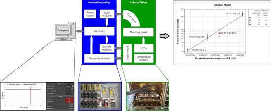
2.1. LED Lifetime Analyzer

In this section, the test setup developed during the study in order to explore the long-term behavior of LEDs is presented. The task presupposes two requirements. First, a large number of LEDs has to be tested in order to attain statistical significance; and second, the tests are taking place under different conditions, particularly at different forward current levels and ambient temperatures (testing in climatic chamber). The emitted light from LEDs, the voltage change at the LED, and the temperature at its solder joint need to be monitored over a long period of time. In order to tackle these challenges simultaneously and to solve these subtasks separately, the test setup had to be separated into several modules, which are connected to the mainboard. Figure 1 provides an overview of the complete setup, including its submodules.
A computer is used to define the current levels and configure the layout. A communication circuit between this computer and the actual test system needs to be set in order to send and receive data. The test setup consists of a microcontroller mounted on the mainboard and the measuring boards. The software “LED Lifetime Analyzer”, which was developed in-house, represents the human–machine interface (HMI). Furthermore, two power supply units are responsible for the energy supply needed to operate the LEDs and to conduct the measurement. A cable connection to the external setup provides the LEDs with current and assures the measurement of the voltage and the temperature. Consequently, the external setup is separated from the actual test setup for the purpose of protecting the measurement boards not only against external influences, but mainly also against the high temperature in the climatic chamber. Additionally, optical fibers ensure the light coupling from the LEDs back to the light modules mounted on the test setup. The structure and the concept of the test setup and the associated boards are presented in the following subsections.

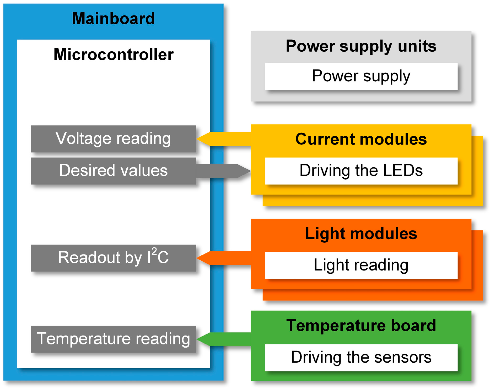
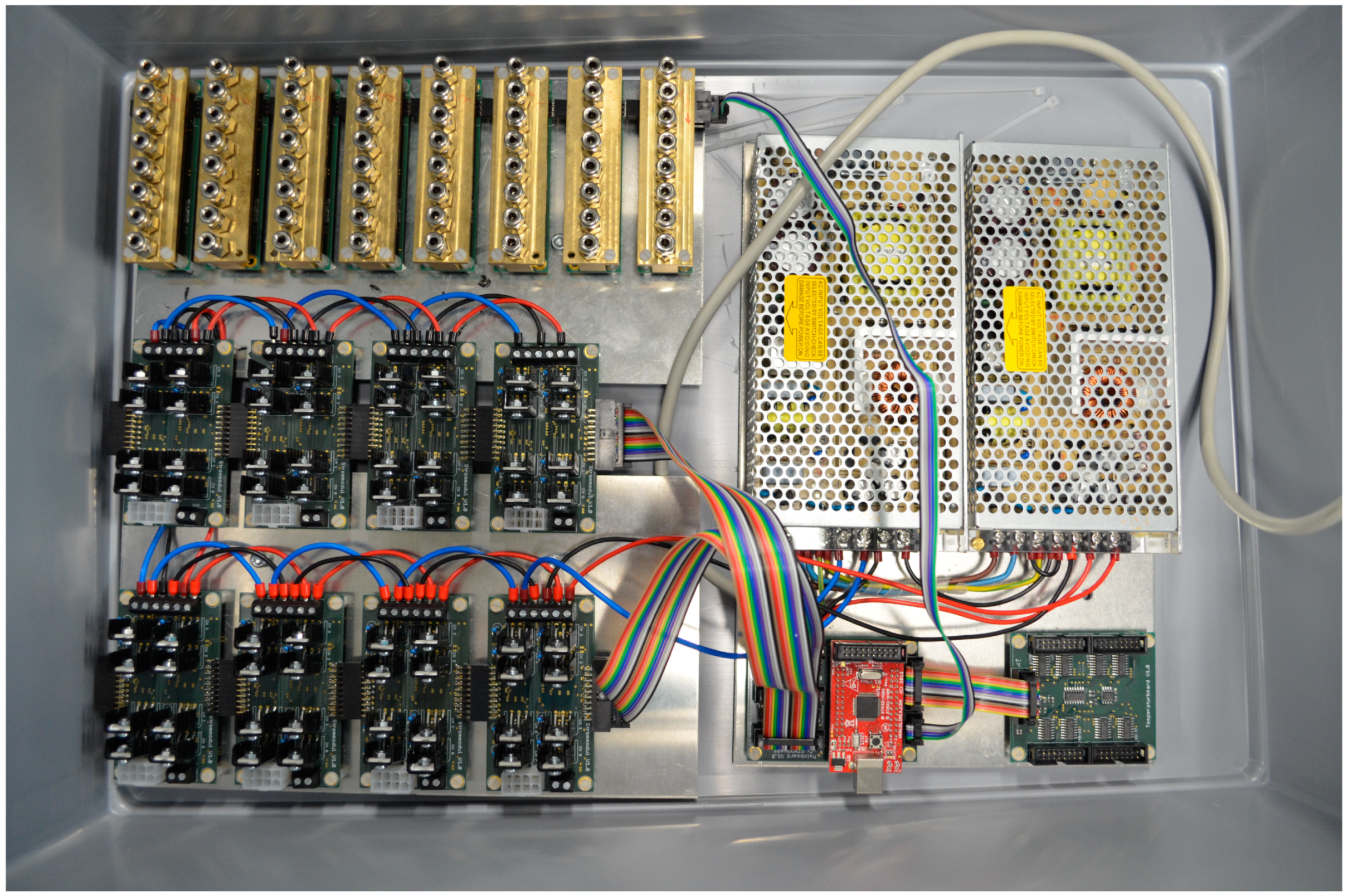
2.1.1. The Test Setup

The focus of this section is on the development of the test system, which is composed of the different components and boards. Figure 2 shows the signal flow and the task breakdown for each and every module.
As already mentioned before, the mainboard takes over the controlling role. In addition to this compulsory part, up to 8 current modules can be integrated to the test system, each one of them assume the control of up to 8 LEDs with a prespecified current level. This means that a maximum of 64 LEDs can be powered and controlled by the test setup at the same time. The current modules also incorporate multiplexers and voltage taps on the terminals of all LED contact pads. This allows the voltage measurement of each LED. Up to 8 light modules, equipped with 8 light sensors each, grant the measurement of the emitted light. Fiber optics guide the captured illuminance to reach the light sensors mounted on the light modules. Via an I2C bus, the measured values can be read out by the microcontroller, sitting on the mainboard. Thereby, digital multiplexers are in use to prevent address ambiguity of the sensors. As an interface between software and hardware, the development board STM32-H405 by Olimex is used. This board houses an STM32F405RGT6 microcontroller based on an ARM® Cortex® M4 processor, produced by STMicroelectronics. Along with this microcontroller, the mainboard represents the central communication, measurement, and control element of the test setup. All other boards are connected to the mainboard via ribbon cables, which is why this board is indispensable for the function of the test setup. The tasks of the mainboard are:
  • Housing the microcontroller and its peripherals, as well as logic;
  • Hardware power supply with +5 V, −5 V, and +3.3 V;
  • Serial communication with the control software via a USB cable;
  • Switching the digital and analog multiplexers;
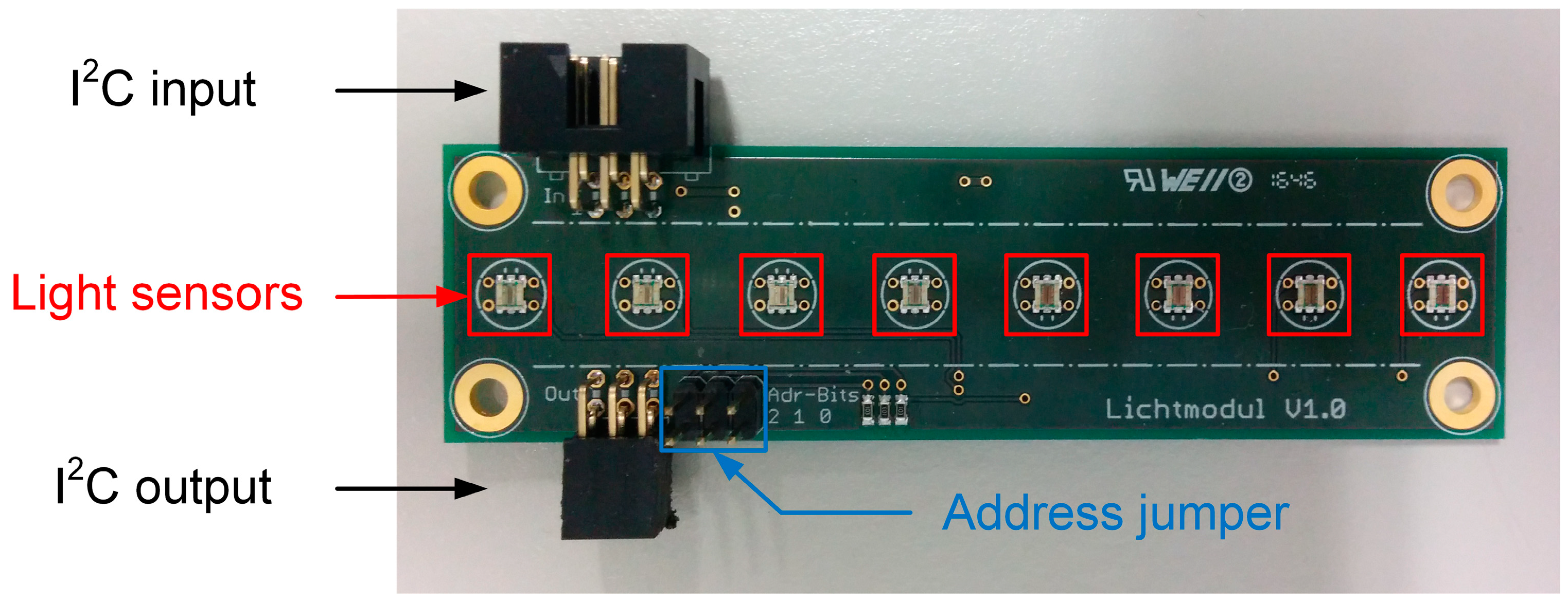
  • Reading the values coming from the light sensors via the I2C bus;
  • Analog-to-digital conversion for the voltage and temperature measurement;
  • Control of the constant current levels by providing the appropriate analog control voltages.
Figure 3 illustrates the task distribution of the mainboard. Figure 4 shows the top view of the mainboard with no microcontroller mounted on it, and the connections to different modules are marked.
The main task of the current module is to provide the LEDs with a predefined current profile. It constitutes of 8 LED drivers, each one in the form of a voltage-controlled constant current source. In total, up to 8 current modules can be integrated.
Figure 5 shows the basic function of the developed module. The input signals PROF_0 to PROF_7 represent the 8 analog control voltages specified by the mainboard. With these, the current sources I_OUT_0 to I_OUT_7 can be individually controlled and adjusted. In addition, a tapping of the LED voltages VOLT_0 to VOLT_7 via a voltage divider and a subsequent multiplexer takes place at these terminals. This output voltage VOLT_X is fed back to the mainboard, where it is analog-to-digital converted.
The signal lines PROF_MUX_CH0, PROF_MUX_CH1 and PROF_MUX_CH2 take over the addressing of the voltages VOLT_0 to VOLT_7.
Each set of 4 modules together makes up a group, with the test system supporting up to 2 groups. The first module of each group has a socket connector, which is intended for a ribbon connection leading to the mainboard. The other 3 current modules of a group are coupled together through their inputs. This allocation into groups is necessary to reduce the complexity of the current modules. Figure 6 shows the different inputs and outputs of a current module.
The temperature board assumes the measurement of up to 64 temperature values by means of platinum resistors. To this end, a constant current source based on an operational amplifier is installed on the board. In addition, there are 8 analog profile multiplexers MUX 0–7 and one analog board multiplexer MUX to evaluate all 64 channels with an analog-to-digital converter (ADC). In order to increase the voltages at the measuring resistors, a non-inverting amplifier is implemented. For the measurement, the used Pt100 resistors (R0 = 100 Ω at a temperature of T = 0 °C) are operated by the constant current source with a current of IMeasure = 1 mA and connected through multiplexers. This is shown schematically in Figure 7. The resulting voltage UMeasure is amplified to the voltage UADC, which is converted in the ADC into the digital value DTemp. This value is used to calculate the temperature. The digital inputs BRD_MUX_CH0 to BRD_MUX_CH2 and PROF_MUX_CH0 to PROF_MUX_CH2 are respectively the address lines for the board and the profile multiplexer. The top view of the temperature board is presented in Figure 8.
The light module is the central element of the test system and houses 8 light sensors atop. Up to 8 different modules can be integrated. This makes it possible to measure the emitted light of the requested 64 LEDs under test. The light sensors of the light module are digital ambient light sensors (ALS) with an I2C interface. They measure the illuminance Ev, LEDx, which is brought over from the tested LEDs coaxially through the fiber optics. Figure 9 shows a schematic block diagram of the light module.
Via a connection block, the optical mapping takes place on the light sensors ALS 0 to ALS 7. They measure the illuminance via broadband and infrared photodiodes and convert them into two digital measured values, DCh0 and DCh1. These values can be read out by the mainboard, connected via ribbon cable, via the I2C bus. SDA (Serial Data) denotes the data line and SCL (Serial Clock) the clock line. VDD and VSS denote the positive and negative supply voltage for the sensors and multiplexers. These are provided by the mainboard. Figure 10 shows a light module in top view without the connection block for the fiber optics. The digital I2C input of the first light module leads to the mainboard. All other light modules can be connected by coupling the digital I2C input to the digital I2C output of the previous light module.
Figure 11 provides an overview of the built-up assembly of the complete test setup.

2.1.2. The Software

In the course of this work and in order to operate the test setup for investigating the lifetime of LEDs, the application software was coded in C# 6. It gives the user the opportunity to configure the different modules of the system. In addition, this software graphically displays the present state of the LEDs and the current measurement values of the test. Furthermore, it stores the measurement data permanently in a readable format on the hard disk. Thus, the program outlines the human–machine interface of the test setup.
The software offers the possibility to define different current profiles, such as constant, step, or even piecewise linear profiles. These describe a cyclical run of the current ITarget over an adjustable period Tcycle. Each current profile is also assigned to a measuring time tMeasure, at which the measured value is periodically recorded. This ensures that the measurements always take place at the same current level. Predefined are up to 8 current profiles, each one of which can be selected from the different types of profiles presented before. For this work, only the constant current profile, shown in Figure 12, was applied, according to the standards [4,5]. In order to properly make use of the microcontroller mentioned in Section 2.1.1, a firmware was coded mainly in C++ and partly in C. The main task of the firmware is the direct access to the periphery of the microcontroller.
Another task of the device-side firmware is the communication with the application software via USB. On the one hand, it enables a data transfer from the device to the LED Lifetime Analyzer software; while on the other hand, it also assures the configuration of the test system itself. Beyond that, the firmware provides the logic as well as the measuring routines and, thus, conducts the actual measuring procedure. The lifetime test is described in the firmware using the discrete system state shown in Figure 13. A distinction is made between system states and substates. While the system states describe the present state of the whole sequence, the substates provide information about the status of the current system state. Each system state initially starts with the attribute “Active” and can change either to the substate “Successful” or, in the event of an error, to the state “Error”. Only when a system state is successfully completed can the next system state be switched on.
The firmware starts with the state “Starting up”, which is activated with the microcontroller start. This involves the initialization of the periphery, the instantiation of the measurement objects, and the creation of the data structure.
This is followed by the “Calibrating Temperature” state, in which the fault resistances of the multiplexers and the connection cables to the temperature sensors are determined. During the next system state “Calibrating Reference”, the initial reference values of the LEDs for the illuminance Ev and the electrical forward voltage UF are stored. As soon as the reference run has been completed successfully, the system switches to the test run after confirmation from the user (running test). This describes the life test of the LED, in which the current profiles run in an infinite loop. During the test, the user will see the status of each LED in the LED Lifetime Analyzer software, which is graphically highlighted in the event of a failure. The test run is active until the user exits the system.

2.2. Experimental Procedure

The manufacturing process of molded interconnect devices by means of the laser direct structuring method implies the following steps. First, the laser structuring is performed on the injection molded part. This part must contain laser-activatable additives [24]. The selective metallization or, more precisely, the electroless plating process follows after a cleaning step. In the case of higher power flux and, therefore, thicker metallization layers required, an additional electroplating step is carried out. Typically, a copper layer (about 7 µm), responsible for the electrical conduction, a nickel layer (about 7 µm) as a diffusion barrier, and a gold layer as surface finish (about 0.1 µm) are deposited [21]. The tested LED has a maximum forward current of 25 mA and a viewing angle of 120° and features a dominant wavelength equal to 470 nm (blue). By a current of 20 mA, the forward voltage value is 3.2 V (64 mW electrical Power). The developed system can be used to test any other kind of LED having comparable characteristics. For this work, the considered MID substrates were made of the thermoplastic TECACOMP® PPA LDS black 4109 V, known for good thermal conductivity. An example of the used test specimen is illustrated in Figure 14.
To find out the relevant process steps, this experimental study was scheduled using the statistics software Minitab. Table 1 presents the full factorial design of experiments and shows the relevant factors and their corresponding stages. These stages have been defined after many experimental trials under different test conditions, in order to prevent overstressing, and consequently, to address the same failure mechanism. The fact that the ambient temperature and the forward current impact the junction temperature of the LED is well-known [25]. Higher current levels engender higher levels of heat dissipated at the junction. The ambient temperature has a similar impact. Therefore, this temperature should be held as low as possible, otherwise unwanted effects can arise. These can deteriorate the reliability and lead to a shorter lifetime and even to color shift in the LED [25]. Additionally, it is worth underlining that the temperature measured by the temperature sensors, mentioned in Section 2.1, was evenly distributed across the climatic chamber. This confirms the fact that all LEDs are tested under the same conditions. In order to consider the junction temperatures in the lifetime model, thermal measurements by means of a thermographic camera were carried out. Thereby, initial maximum temperatures at the LEDs, which narrowly correlate with the junction temperatures, were measured. A key parameter for this type of measurement is emissivity. The emissivity ε depends not only on the surface finish, but also on its color [26]. In order to consider this effect, a comparative calibration approach using a black coating, with a homogeneous emissivity of about 0.97, was conducted. Emissivity values of about 0.96 were measured. In Figure 14, an example of a thermographic image taken by an IR camera is illustrated. The minimum pitch between two neighboring LEDs is about 15 mm. Figure 15 presents the external setup in the climatic chamber, with test substrates and fiber optics adjusted through the mounting sheet. Note that the fiber optics and all the cables used were selected by reason of their temperature resistance.

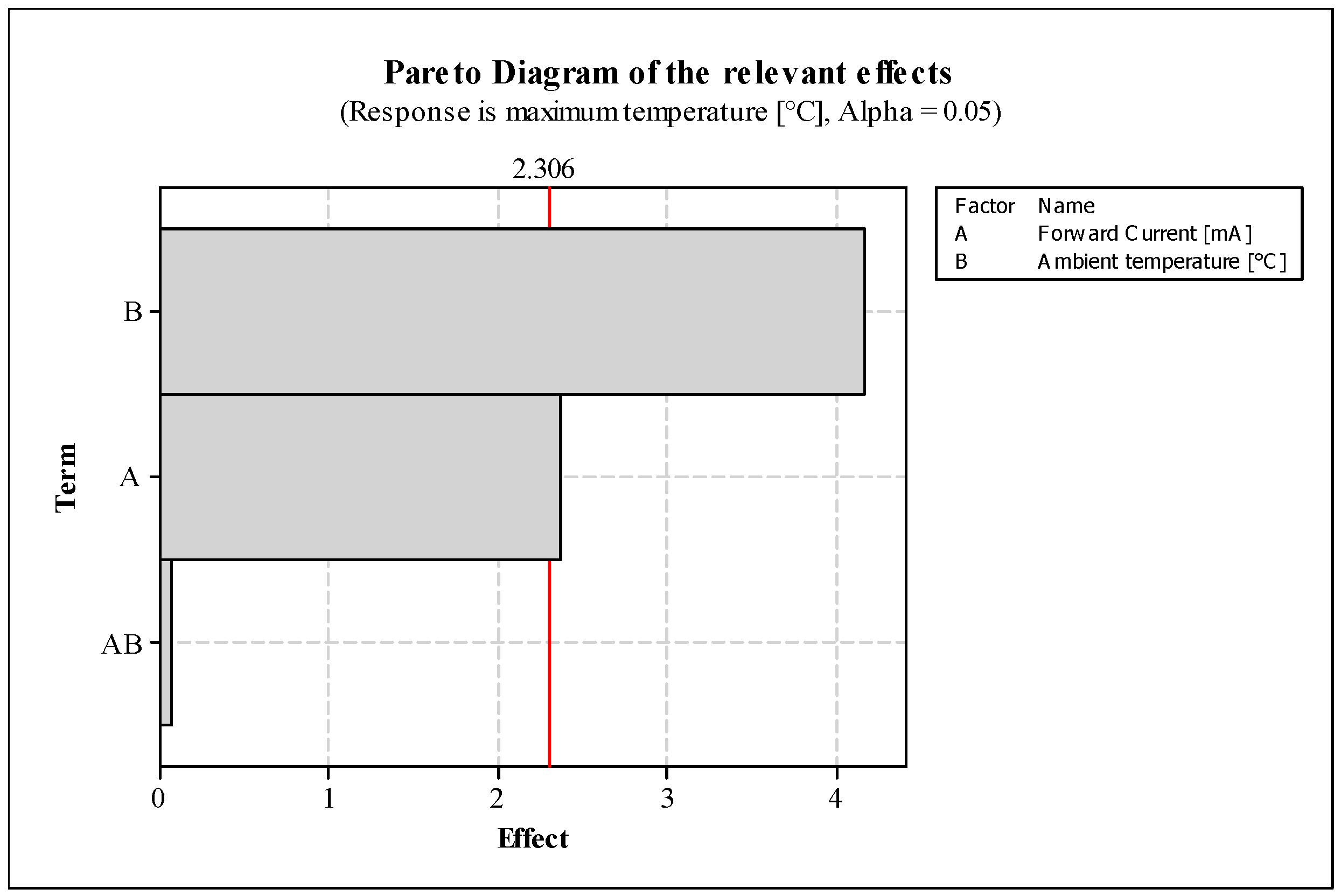
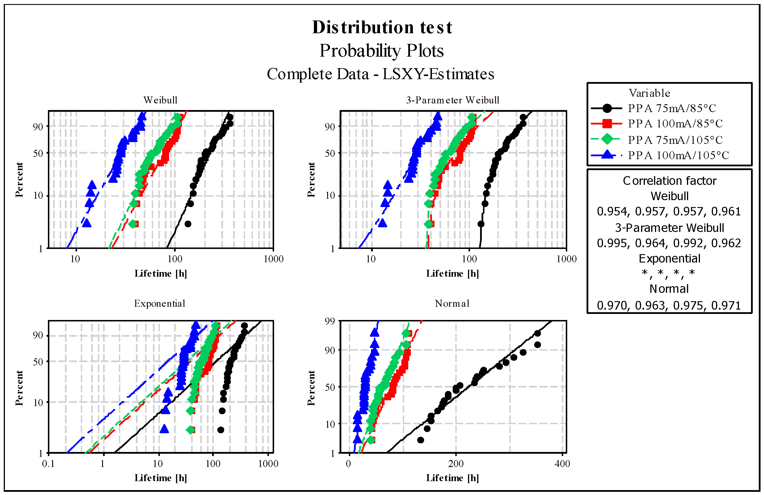
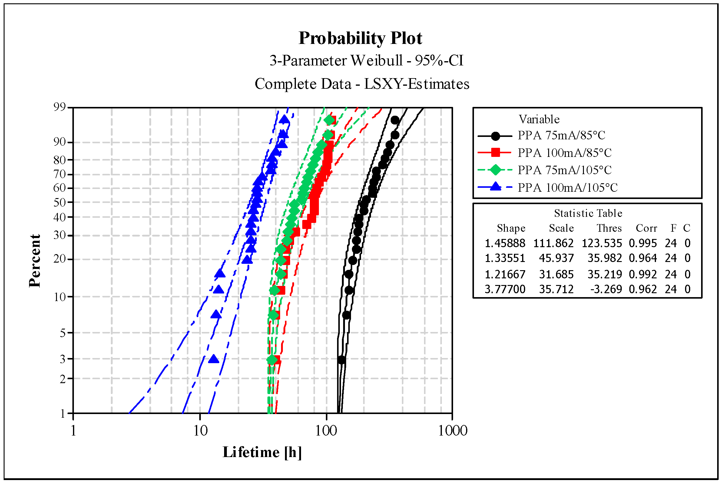
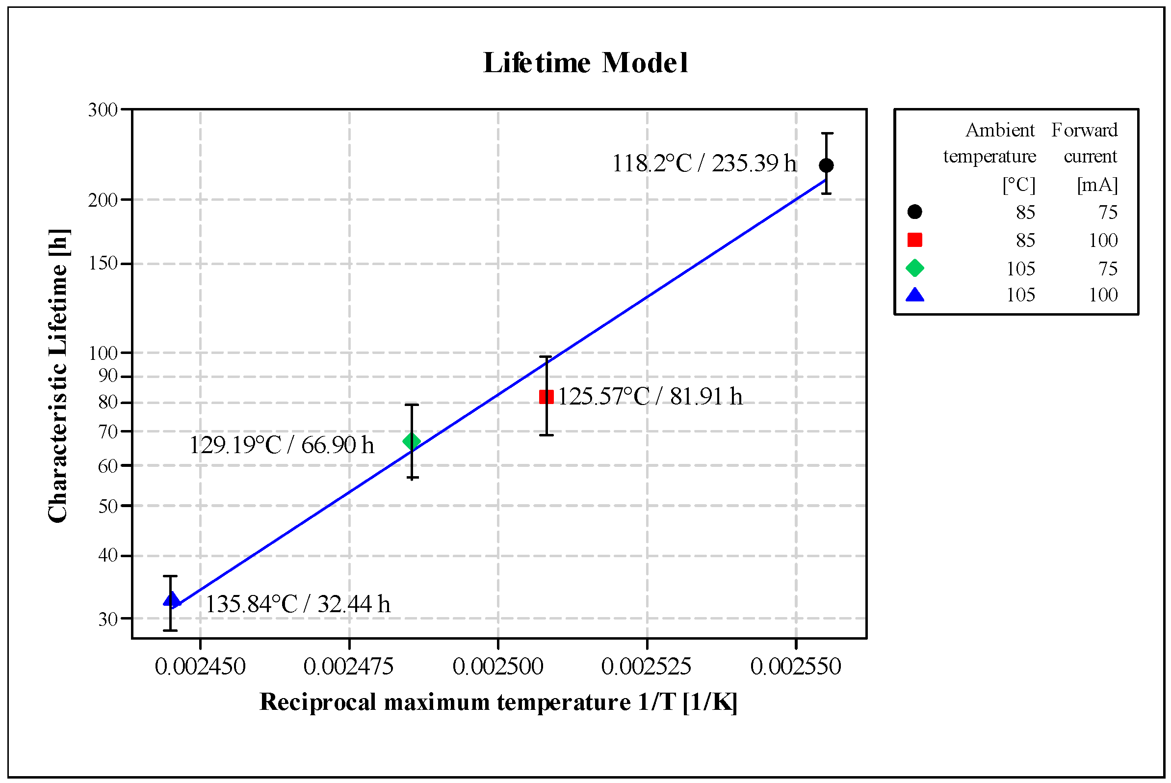
3. Results and Discussion

The focus of this paper lies on the development of the test setup (Section 2). Therefore, and in order to validate it, some results obtained by using it are introduced and discussed in the following section. More detailed results, taking into consideration the effect of the substrate material and the real junction temperatures measured by means of transient thermal test methods, are presented in Reference [24]. As shown in the Pareto diagram of the relevant effects, illustrated in Figure 16, the investigated factors have a significant influence on the maximum temperature at the LED, unlike their combined effect.
This behavior confirms previously gained findings and is consistent with the results from earlier investigations [16,17,24]. The main effects plot for the maximum temperature, shown in Figure 17, validates these observations and shows that the difference between the two ambient temperatures stages has the higher impact (steeper slope). Afterwards, tests were carried out using the test setup introduced in Section 2. By way of example, Figure 18 reports the relative illuminance vs. time dependence for LEDs from each constellation. It comes out that after an initial stage, where the illuminances decrease rapidly, the aging process downshifts and attains a constant value. The test was conducted until all LEDs had crossed the failure criterion L70. During this test, the failure criterion U110, the case of the voltage surpassing the barrier of 110%, did not occur.
After the evaluation of the gained results, a distribution test was carried out. The test results, illustrated in Figure 19, indicate that the three parameter Weibull distribution shows in three of four cases the best correlation factors. This can already be detected on the bent curve in the probability network of the Weibull distribution with two parameters. This is due to a failure-free time [27].
For the exponential distribution, no correlation coefficients could be determined. This indicates that no direct relationship was detected between the lifetime data and this art of distribution. This is comprehensible, since with the exponential function the early failures, with falling failure rates, can be described. Figure 20 contains the Weibull plots for the considered constellations, including statistical lifetime parameters and 95% lower and upper confidence intervals. A shape factor of more than one indicates some aging behavior. These shape factors, which vary from 1.21 up to 1.45, indicate a similar failure mechanism. Investigations dealing with the analysis of these failure mechanisms, by means of X-ray, transient thermal testing, and cross-section, were carried out and confirmed that the delamination of the die attach is the most frequently occurring failure mechanism [24].
The characteristic lifetime LT was determined at 63.21%, in accordance with Reference [28]. It is the time at which 63.21% of the LEDs failed. In Figure 21, the main effects plot and the interaction plot for the characteristic lifetime are shown. Corresponding to the main effects plots in both figures, Figure 17 and Figure 21, it is clearly perceptible that both applied stresses, forward current and ambient temperature, have almost the same, but opposite leverages on maximum temperature T and the characteristic lifetime. For this reason, it can be underlined that both outcomes correlate with each other. Higher forward current levels lead to higher maximum temperature, and consequently, to a shorter lifetime. The same applies for the effect of the ambient temperature. Usually, an Arrhenius-type equation is used to estimate the lifetime of a component subjected to thermal effects [29]. The developed lifetime model, presented in Figure 22, seems to obey this rule, since the determination coefficient R2 is 0.9846. This underlines the excellent fitting quality. Hence, the characteristic lifetime LT fits the following expression:
L T = C T e E A k T
where CT = 5 × 10⁻⁵ is the thermal factor, EA = 1.523 eV is the activation energy, k = 8.617385 × 10⁻⁵ eV·K−1 is the Boltzmann constant, and T is the maximum absolute temperature in Kelvin.

4. Conclusions

The aim of this work was, amongst others, the development of a test setup that can be used to investigate the aging of different LEDs on different MID substrates and even on conventional substrates, such as printed circuit boards (PCB). It was required to monitor the physical LED properties, more precisely the illuminance, the temperature at the solder joints, and the electrical forward voltage, in order to estimate their lifetime. Another requirement was the ability to test the LEDs in a climatic chamber under harsh environmental conditions. The test system developed in the course of this work fulfills these tasks and enables the simultaneous life test of many LEDs (up to 64 LEDs), which is a prerequisite for a statistically valid accuracy.
Reliability studies and accelerated lifetime tests under combined stress conditions (higher ambient temperatures and forward current levels) were conducted in order to validate the test setup. The obtained results as well as the developed lifetime model were illustrated and discussed. It has been presented that the proposed lifetime model, reporting the relationship between maximum temperature and characteristic lifetime, suits very well with the Arrhenius equation. A determination coefficient R2 of 0.9846 highlights the excellent fitting quality.
Further works dealing with simulation approaches with a view to optimizing the experimental effort of measuring the temperature of all LEDs are currently under investigation.

Author Contributions

M.S. designed the test setup, conducted the experiments, analyzed the resulting parts, and wrote the manuscript. M.F. developed the test setup and programmed the software. R.K. and T.G. supported the execution of the experiments and revised the manuscript. R.M. supported the development of the test setup. A.Z. revised the manuscript, supervised the project, and provided the funding.

Funding

This research received no external funding.

Conflicts of Interest

The authors declare no conflict of interest.

References

  1. EIAJ ED-4701/100 Standard of Japan Electronics and Information Technology Industries Association. Environmental and Endurance Test Methods for Semiconductor Devices. Japan. 2001. Available online: https://home.jeita.or.jp/tsc/std-pdf/ED-4701_400-1.pdf (accessed on 4 December 2018).
  2. STEADY-STATE TEMPERATURE-HUMIDITY BIAS LIFE TEST | JEDEC. Available online: https://www.jedec.org/standards-documents/docs/jesd-22-a101c (accessed on 1 July 2018).
  3. JEDEC Solid State Technology Association. JEDEC Standard No. 22-A108D: Temperature, Bias, and Operating Life; JEDEC: Arlington, VA, USA, 2010. [Google Scholar]
  4. DIN EN IEC 62663-2—Non-ballasted LED lamps—Performance requirements (IEC 34A/1601/CD:2012); Deutsches Institut für Normung—German Institute for Standardization: Berlin, Germany, 2012.
  5. DIN EN IEC 62717:2014 + AMD1:2015 CSV—LED modules for general lighting—Performance requirements; Deutsches Institut für Normung—German Institute for Standardization: Berlin, Germany, 2015.
  6. Chen, C.H.; Tsai, W.L.; Tsai, M.Y. Thermal resistance and reliability of low-cost high-power LED packages under WHTOL test. In Proceedings of the 2008 International Conference on Electronic Materials and Packaging, Taibei, Taiwan, 22–24 October 2008; pp. 271–276. [Google Scholar]
  7. Solid State Lighting Reliability: Components to Systems; Van Driel, W.D.; Fan, X. (Eds.) Solid State Lighting Technology and Application Series; Springer: New York, NY, USA, 2012; ISBN 978-1-4614-3066-7. [Google Scholar]
  8. Van Driel, W.D.; Fan, X.; Zhang, G.Q. Solid State Lighting Reliability Part 2: Components to Systems; Springer: Cham, Switzerland, 2018; ISBN 978-3-319-58175-0. [Google Scholar]
  9. Thermal Management for LED Applications; Lasance, C.J.M.; Poppe, A. (Eds.) Solid State Lighting Technology and Application Series; Springer: New York, NY, USA, 2014; Volume 2, ISBN 978-1-4614-5091-7. [Google Scholar]
  10. Lu, G.; Yang, S.; Huang, Y. Analysis on failure modes and mechanisms of LED. In Proceedings of the 2009 8th International Conference on Reliability, Maintainability and Safety, Chengdu, China, 20–24 July 2009; pp. 1237–1241. [Google Scholar]
  11. Guoguang, L.; Yun, H.; Yunfei, E.; Shaohua, Y.; Zhifeng, L. The relationship between LED package and reliability. In Proceedings of the 2009 16th IEEE International Symposium on the Physical and Failure Analysis of Integrated Circuits, Suzhou, China, 6–10 July 2009; pp. 323–326. [Google Scholar]
  12. Albertini, A.; Masi, M.G.; Mazzanti, G.; Peretto, L.; Tinarelli, R. A test set for LEDs life model estimation. In Proceedings of the 2010 IEEE Instrumentation & Measurement Technology Conference, Austin, TX, USA, 3–6 May 2010; pp. 426–431. [Google Scholar]
  13. Albertini, A.; Masi, M.G.; Mazzanti, G.; Peretto, L.; Tinarelli, R. Experimental Analysis of LEDs’ Reliability Under Combined Stress Conditions. In Proceedings of the 2011 IEEE International Instrumentation and Measurement Technology Conference, Binjiang, China, 10–12 May 2011. [Google Scholar]
  14. Nogueira, E.; Orlando, V.; Ochoa, J.; Fernandez, A.; Vazquez, M. Accelerated Life Test of high luminosity blue LEDs. Microelectron. Reliabil. 2016, 64, 631–634. [Google Scholar] [CrossRef]
  15. Albertini, A.; Mazzanti, G.; Peretto, L.; Tinarelli, R. Development of a Life Model for Light Emitting Diodes Stressed by Forward Current. IEEE Trans. Reliabil. 2014, 63, 523–533. [Google Scholar] [CrossRef]
  16. Soltani, M.; Kulkarni, R.; Liu, Y.; Barth, M.; Groezinger, T.; Zimmermann, A. Experimental and computational study of array effects on LED thermal management on molded interconnect devices MID. In Proceedings of the 2018 13th International Congress Molded Interconnect Devices (MID), Wurzburg, Germany, 25–26 September 2018; p. 6. [Google Scholar]
  17. Barth, M.; Kulkarni, R.; Soltani, M.; Eberhardt, W.; Meißner, T.; Zimmermann, A. Heat dissipation for MID applications in lighting technology. In Proceedings of the 2016 12th International Congress Molded Interconnect Devices (MID), Wurzburg, Germany, 28–29 September 2016; pp. 1–4. [Google Scholar]
  18. Leneke, T.; Schmidt, B. Entwärmungskonzepte durch funktionale Strukturen in spritzgegossenen dreidimensionalen Schaltungsträgern; Berichte aus der Elektrotechnik; 1. Aufl.; Shaker: Aachen, Germany, 2013; ISBN 978-3-8440-1688-8. [Google Scholar]
  19. Heinle, C. Simulationsgestützte Entwicklung von Bauteilen aus wärmeleitenden Kunststoffen; Universität Erlangen-Nürnberg: Erlangen, Germany, 2012. [Google Scholar]
  20. Heinle, C. Development and Production of highly integrated LED-Systems with Thermal Conductive Polymers by (Assembly-) Molding. In Proceedings of the Workshop three-dimensional arrangement of LEDs, Bregenz, Austria, 25 September 2013. [Google Scholar]
  21. Groezinger, T. Untersuchungen zu Zuverlässigkeit und Lebensdauermodellen für gelötete SMD auf spritzgegossenen Schaltungsträgen. Ph.D. Thesis, Institute for Micro Integration, University of Stuttgart, Stuttgart, Germany, 2015. [Google Scholar]
  22. Wild, P.; Groezinger, T.; Lorenz, D.; Zimmermann, A. Void Formation and Their Effect on Reliability of Lead-Free Solder Joints on MID and PCB Substrates. IEEE Trans. Reliabil. 2017, 66, 1229–1237. [Google Scholar] [CrossRef]
  23. Wild, P.; Lorenz, D.; Groezinger, T.; Zimmermann, A. Effect of voids on thermo-mechanical reliability of chip resistor solder joints: Experiment, modelling and simulation. Microelectron. Reliabil. 2018, 85, 163–175. [Google Scholar] [CrossRef]
  24. Soltani, M.; Freyburger, M.; Kulkarni, R.; Mohr, R.; Groezinger, T.; Zimmermann, A. Reliability study and thermal performance of LEDs on molded interconnect devices (MID) and PCB. Multidiscip. Open Access J. IEEE Access 2018, 11, 51669–51679. [Google Scholar] [CrossRef]
  25. Chang, M.-H.; Das, D.; Varde, P.V.; Pecht, M. Light emitting diodes reliability review. Microelectron. Reliabil. 2012, 52, 762–782. [Google Scholar] [CrossRef]
  26. Svasta, P.; Simion-Zanescu, D.; Ionescu, R. Components’ emissivity in reflow soldering process. In Proceedings of the 2004 54th Electronic Components and Technology Conference (IEEE Cat. No. 04CH37546), Las Vegas, NV, USA, 4 June 2004; Volume 2, pp. 1921–1924. [Google Scholar]
  27. Bertsche, B.; Lechner, G. Zuverlässigkeit im Fahrzeug- und Maschinenbau: Ermittlung von Bauteil- und System-Zuverlässigkeiten; VDI; 3. überarb. und erw. Aufl.; Springer: Berlin, Germany, 2004; ISBN 978-3-540-20871-6. [Google Scholar]
  28. Bertsche, B.; Göhner, P.; Jensen, U.; Schinköthe, W.; Wunderlich, H.-J. Zuverlässigkeit mechatronischer Systeme: Grundlagen und Bewertung in frühen Entwicklungsphasen; VDI; Springer: Berlin, Germany, 2009; ISBN 978-3-540-85089-2. [Google Scholar]
  29. Hartzell, A.L.; da Silva, M.G.; Shea, H.R. Lifetime Prediction. In MEMS Reliability; Springer: Boston, MA, USA, 2011; pp. 9–42. ISBN 978-1-4419-6017-7. [Google Scholar]
Figure 1. Overview of the test setup.
Instruments 02 00028 g001
Figure 2. Structure of the test system.
Instruments 02 00028 g002
Figure 3. Block diagram of the mainboard.
Instruments 02 00028 g003
Figure 4. Top view of the mainboard.
Instruments 02 00028 g004
Figure 5. Block diagram of the current module.
Instruments 02 00028 g005
Figure 6. Top view of the current module.
Instruments 02 00028 g006
Figure 7. Block diagram of the temperature board.
Instruments 02 00028 g007
Figure 8. Top view of the temperature board.
Instruments 02 00028 g008
Figure 9. Block diagram of the light module.
Instruments 02 00028 g009
Figure 10. Top view of the light module.
Instruments 02 00028 g010
Figure 11. Top view of the assembled test system; current modules (bottom, left), light modules (top, left), temperature board (bottom, right), mainboard (bottom, middle), and the two power supply units (top, right).
Instruments 02 00028 g011
Figure 12. (Left): Current over time by a constant current profile. (Right): Configuration of a constant current profile in the LED Lifetime Analyzer software.
Instruments 02 00028 g012
Figure 13. Discrete system states of the firmware.
Instruments 02 00028 g013
Figure 14. (Left): Example of a test specimen equipped with LEDs. (Right): Thermal image of the test specimen.
Instruments 02 00028 g014
Figure 15. The external setup in the climatic chamber.
Instruments 02 00028 g015
Figure 16. Pareto diagram of the effects with maximum temperature as response.
Instruments 02 00028 g016
Figure 17. Main effects plot and the interaction plot for the maximum temperature at the LEDs.
Instruments 02 00028 g017
Figure 18. Variation of the light intensity over time for each constellation.
Instruments 02 00028 g018
Figure 19. Distribution test with correlation factors for all tested constellations: Weibull, 3-Parameter Weibull, Exponential and Normal distributions.
Instruments 02 00028 g019
Figure 20. Probability plot on the basis of 3-Parameter Weibull distribution, including 95% lower and upper confidence intervals.
Instruments 02 00028 g020
Figure 21. Main effects plot and the interaction plot for the characteristic lifetime.
Instruments 02 00028 g021
Figure 22. Proposed lifetime model, including 95% lower and upper confidence intervals equation. Equation: y = 5 × 10⁻⁵·e17676x; R2 = 0.9846.
Instruments 02 00028 g022
Table 1. Full factorial design of experiments relevant factors and their corresponding stages.
FactorStage LowStage High
Forward current75 mA100 mA
Ambient Temperature85 °C105 °C

