

Utilization of Additive Manufacturing for the Rapid Prototyping of C-Band Radiofrequency Loads

Abstract
:1. Introduction
1.1. Background
1.2. Motivation
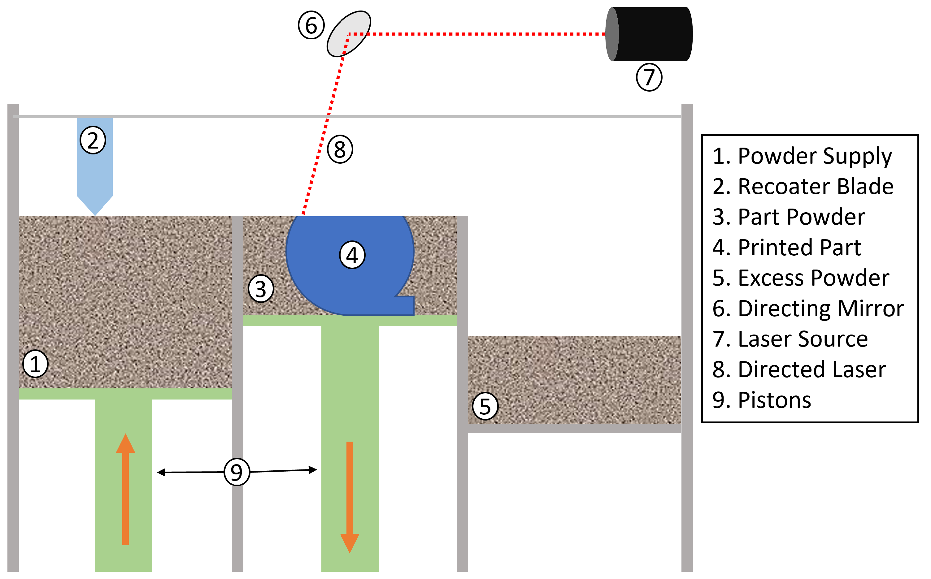
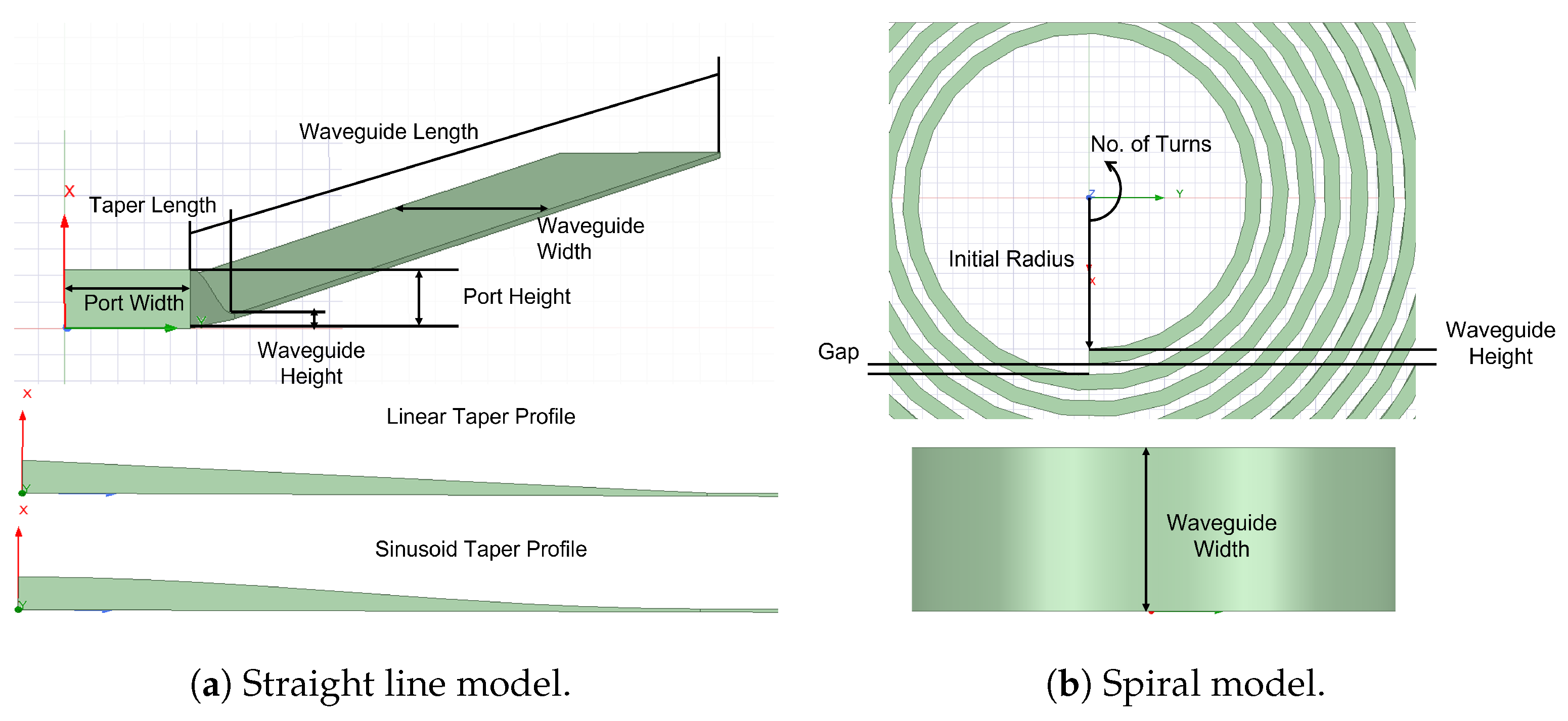
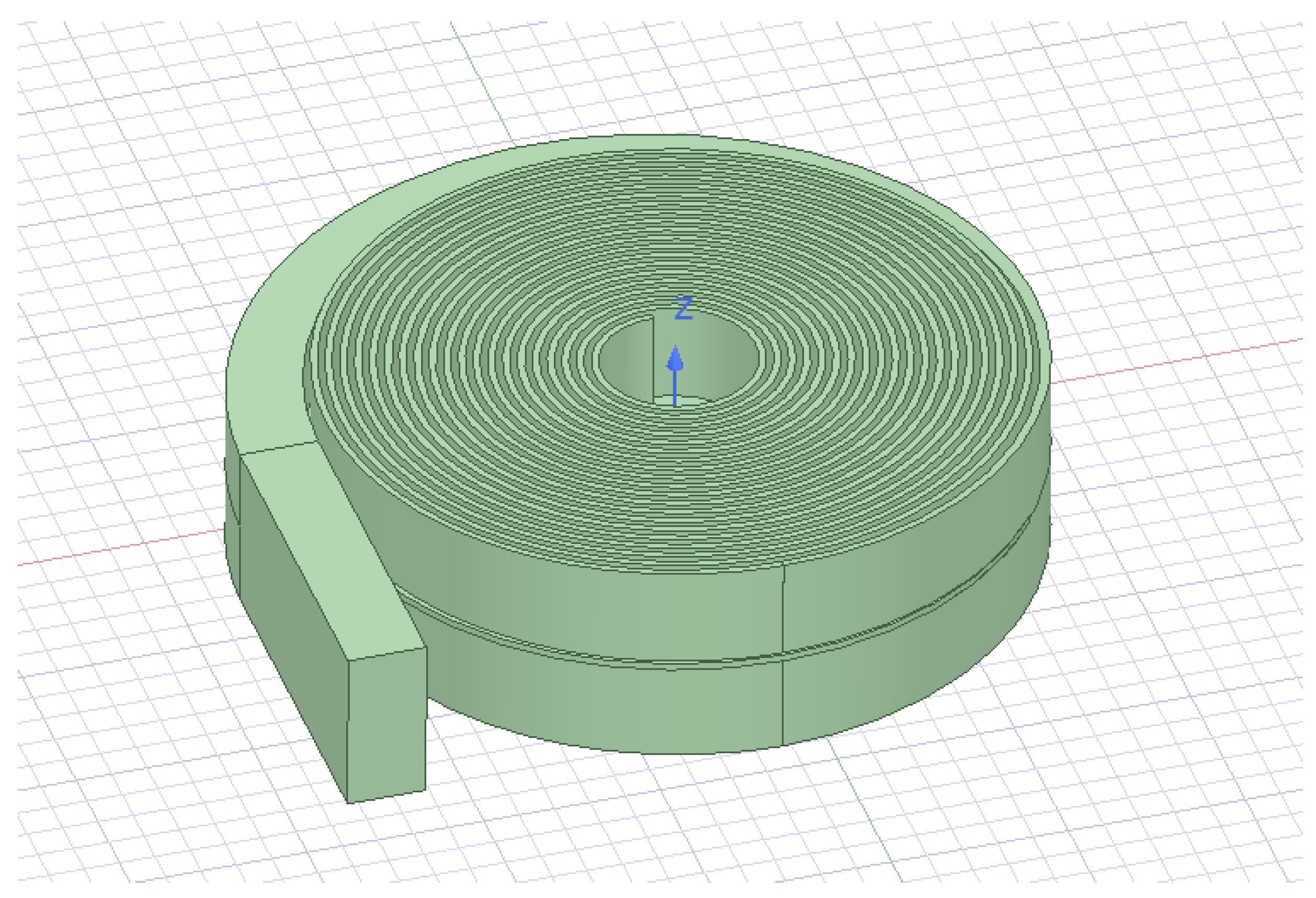
2. Methodology
3. Results
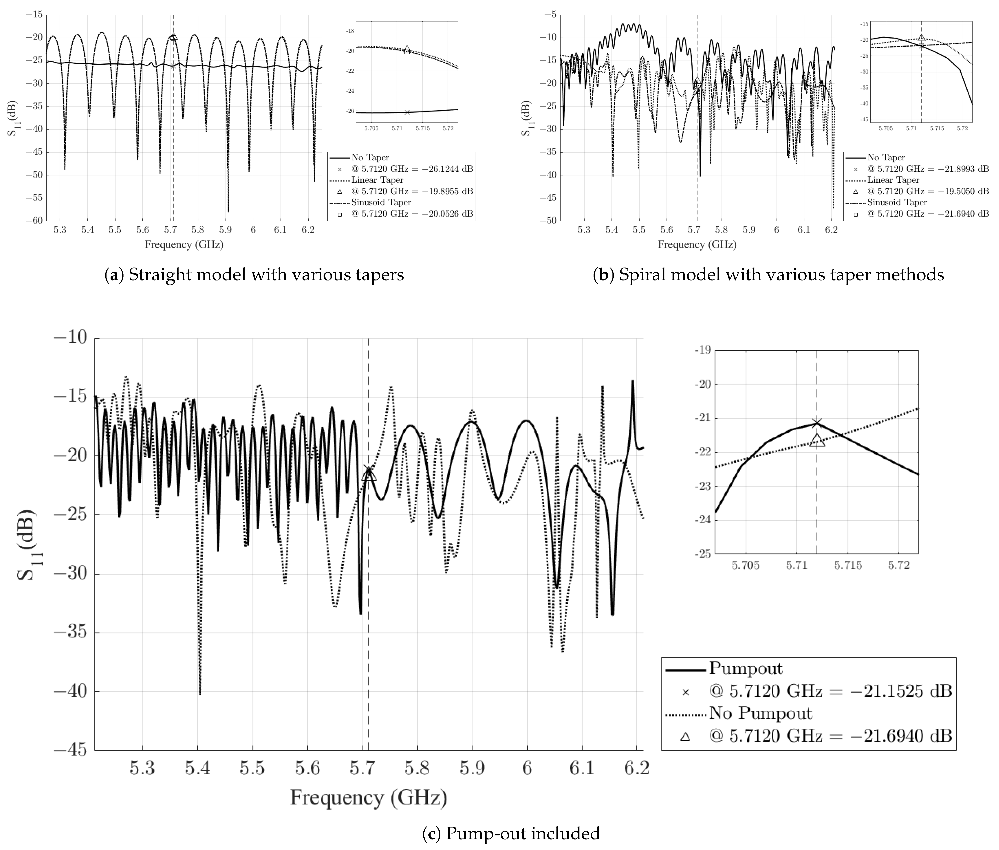
3.1. Simulation Results
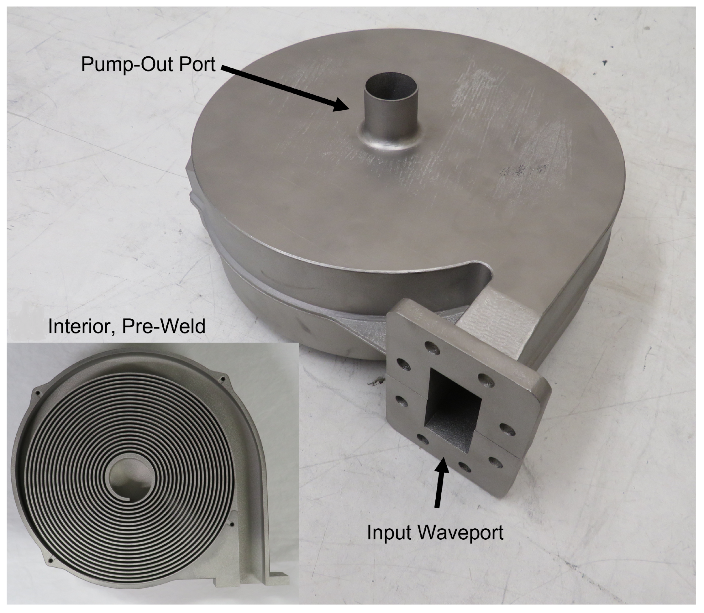
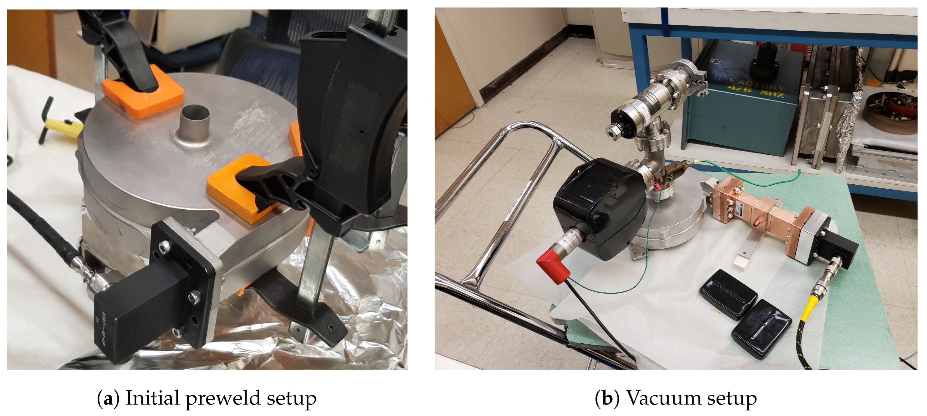
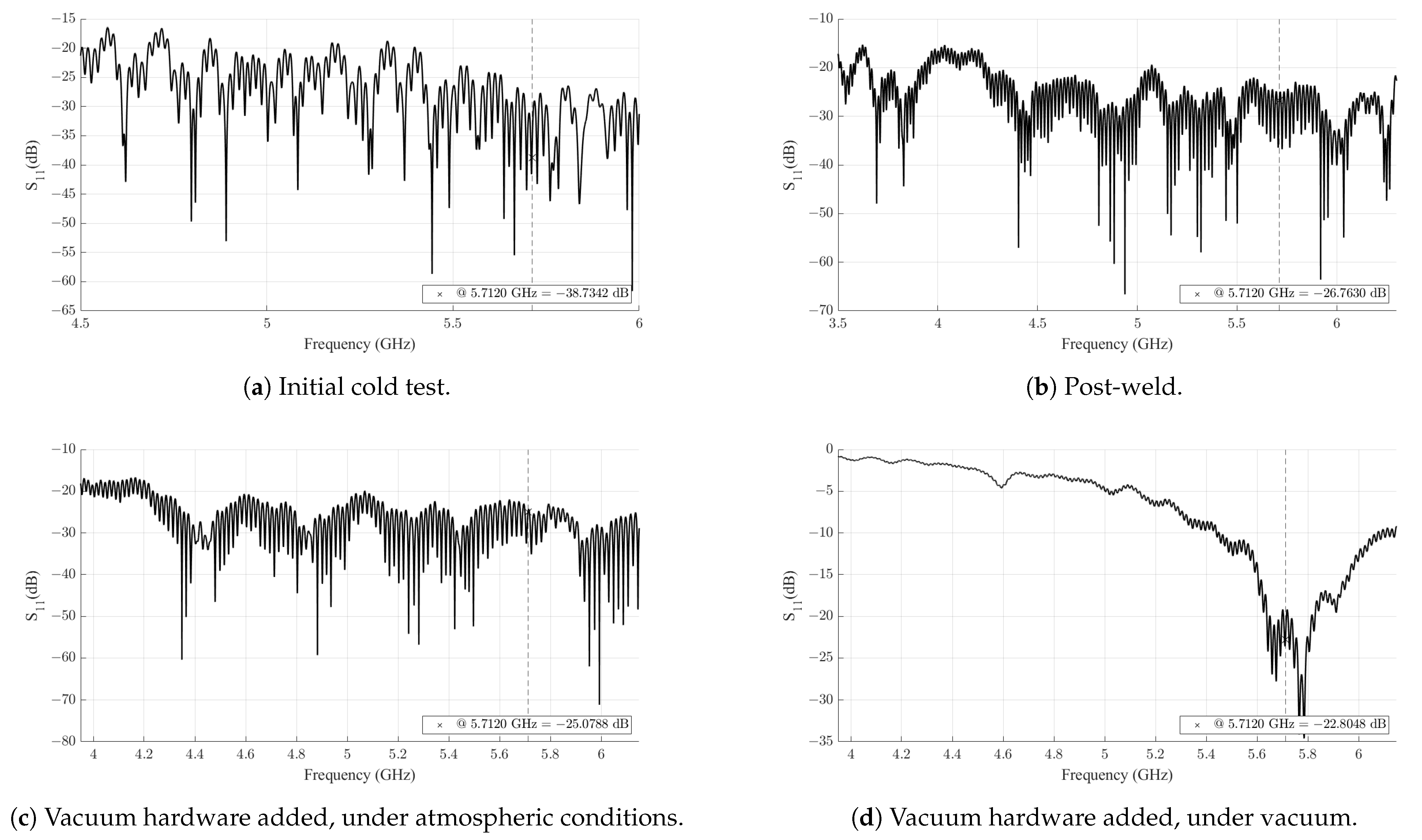
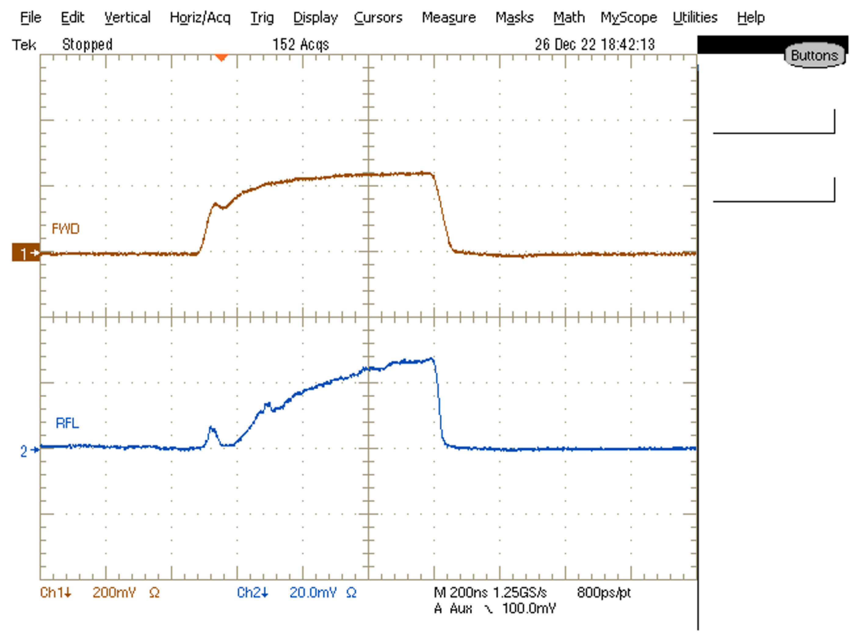
3.2. Printed Model Results
4. Discussion
Author Contributions
Funding
Data Availability Statement
Conflicts of Interest
References
- Ngo, T.D.; Kashani, A.; Imbalzano, G.; Nguyen, K.T.; Hui, D. Additive manufacturing (3D printing): A review of materials, methods, applications and challenges. Compos. Part B Eng. 2018, 143, 172–196. [Google Scholar] [CrossRef]
- Zhang, B.; Guo, Y.X.; Zirath, H.; Zhang, Y.P. Investigation on 3-D-Printing Technologies for Millimeter- Wave and Terahertz Applications. Proc. IEEE 2017, 105, 723–736. [Google Scholar] [CrossRef]
- Wehner, C.; Merrick, J.; Shirley, B.; Weatherford, B.; Mathesen, G.; Nanni, E. RF Properties and Their Variations in a 3D Printed Klystron Circuit and Cavities. arXiv 2022, arXiv:2211.15500. [Google Scholar]
- Bursali, H. X-Band Spiral Load RF Design. 2020. Available online: https://edms.cern.ch/document/2404437/1 (accessed on 8 January 2021).
- Mohd Yusuf, S.; Cutler, S.; Gao, N. Review: The Impact of Metal Additive Manufacturing on the Aerospace Industry. Metals 2019, 9, 1286. [Google Scholar] [CrossRef]
- Chio, T.H.; Huang, G.L.; Zhou, S.G. Application of Direct Metal Laser Sintering to Waveguide-Based Passive Microwave Components, Antennas, and Antenna Arrays. Proc. IEEE 2017, 105, 632–644. [Google Scholar] [CrossRef]
- Svetlizky, D.; Das, M.; Zheng, B.; Vyatskikh, A.L.; Bose, S.; Bandyopadhyay, A.; Schoenung, J.M.; Lavernia, E.J.; Eliaz, N. Directed energy deposition (DED) additive manufacturing: Physical characteristics, defects, challenges and applications. Mater. Today 2021, 49, 271–295. [Google Scholar] [CrossRef]
- Nancharaiah, T. A review paper on metal 3D Printing Technology. In Advances in Materials Processing and Manufacturing Applications: Proceedings of the iCADMA 2020, Jaipur, India, 5–6 November 2020; Springer: Singapore, 2021; pp. 251–259. [Google Scholar] [CrossRef]
- Protolabs. Metal 3D Printing Service. Available online: https://www.protolabs.com/services/3d-printing/direct-metal-laser-sintering/ (accessed on 20 June 2023).
- Franco, D.; Miller Devós Ganga, G.; de Santa-Eulalia, L.A.; Godinho Filho, M. Consolidated and inconclusive effects of additive manufacturing adoption: A systematic literature review. Comput. Ind. Eng. 2020, 148, 106713. [Google Scholar] [CrossRef]
- Davis, T. A deep dive into metal 3D printing. In Proceedings of the Laser 3D Manufacturing VI, San Francisco, CA, USA, 2–7 February 2019; Gu, B., Helvajian, H., Chen, H., Eds.; SPIE: Bellingham, WA, USA, 2019; Volume 10909, p. 1090907. [Google Scholar] [CrossRef]
- Cherdo, L. Metal 3D Printers in 2023: A Comprehensive Guide. 2022. Available online: https://www.aniwaa.com/buyers-guide/3d-printers/best-metal-3d-printer/ (accessed on 9 August 2023).
- Bursali, H. Spiral Loads RF Measurement. 2020. Available online: https://edms.cern.ch/document/2323664/1 (accessed on 28 July 2022).
- Bai, M.; Barklow, T.; Bartoldus, R.; Breidenbach, M.; Grenier, P.; Huang, Z.; Kagan, M.; Lewellen, J.; Li, Z.; Markiewicz, T.W.; et al. C3: A “Cool” Route to the Higgs Boson and Beyond. arXiv 2021, arXiv:2110.15800. [Google Scholar]
- Dasu, S.; Nanni, E.A.; Peskin, M.E.; Vernieri, C.; Barklow, T.; Bartoldus, R.; Bhat, P.C.; Black, K.; Brau, J.; Breidenbach, M.; et al. Strategy for understanding the Higgs physics: The cool copper collider. arXiv 2022, arXiv:2203.07646. [Google Scholar]
- Nanni, E.A.; Breidenbach, M.; Vernieri, C.; Belomestnykh, S.; Bhat, P.; Nagaitsev, S.; Bai, M.; Berg, W.; Barklow, T.; Byrd, J.; et al. C3 Demonstration Research and Development Plan. arXiv 2022, arXiv:2203.09076. [Google Scholar]
- Bane, K.L.; Barklow, T.L.; Breidenbach, M.; Burkhart, C.P.; Fauve, E.A.; Gold, A.R.; Heloin, V.; Li, Z.; Nanni, E.A.; Nasr, M.; et al. An Advanced NCRF Linac Concept for a High Energy e+ e− Linear Collider. arXiv 2018, arXiv:1807.10195. [Google Scholar]
- Protolabs. Designing for Metal 3D Printing. 2019. Available online: https://www.protolabs.com/media/1020535/protolabs_dmls_design_guide.pdf (accessed on 8 August 2023).
- Verploegh, S.; Coffey, M.; Grossman, E.; Popović, Z. Properties of 50–110-GHz Waveguide Components Fabricated by Metal Additive Manufacturing. IEEE Trans. Microw. Theory Tech. 2017, 65, 5144–5153. [Google Scholar] [CrossRef]
- Manafi, S.; Al-Tarifi, M.; Filipovic, D.S. Millimeter-Wave Double-Ridge Waveguide and Components. IEEE Trans. Microw. Theory Tech. 2018, 66, 4726–4736. [Google Scholar] [CrossRef]
- Gallant, L.; Hsiao, A.; Mcsorley, G. Benchmark Physical And Mechanical Property Characterization Of 316L Stainless Steel DMLS Prints. In Proceedings of the Canadian Society for Mechanical Engineering International Congress 2021, Charlottetown, PE, Canada, 27–30 June 2021. [Google Scholar] [CrossRef]


| Variable Name | Symbol | Value (mm) |
|---|---|---|
| Port Width | 47.55 | |
| Port Height | 22.15 | |
| Waveguide Width | 60 | |
| Waveguide Height | 2 | |
| Taper Length | 400 | |
| Waveguide Length | 7000 |
| Variable Name | Symbol | Value | Units |
|---|---|---|---|
| Gap | g | 1.5 | mm |
| Initial Radius | R | 20 | mm |
| No. of Turns | 19.5 | rev | |
| Taper Turn Length | 0.75 | rev |
Disclaimer/Publisher’s Note: The statements, opinions and data contained in all publications are solely those of the individual author(s) and contributor(s) and not of MDPI and/or the editor(s). MDPI and/or the editor(s) disclaim responsibility for any injury to people or property resulting from any ideas, methods, instructions or products referred to in the content. |
© 2023 by the authors. Licensee MDPI, Basel, Switzerland. This article is an open access article distributed under the terms and conditions of the Creative Commons Attribution (CC BY) license (https://creativecommons.org/licenses/by/4.0/).
Share and Cite
Mathesen, G.; Wehner, C.; Merrick, J.; Shirley, B.; Agustsson, R.; Berry, R.; Diego, A.; Nanni, E. Utilization of Additive Manufacturing for the Rapid Prototyping of C-Band Radiofrequency Loads. Instruments 2023, 7, 23. https://doi.org/10.3390/instruments7030023
Mathesen G, Wehner C, Merrick J, Shirley B, Agustsson R, Berry R, Diego A, Nanni E. Utilization of Additive Manufacturing for the Rapid Prototyping of C-Band Radiofrequency Loads. Instruments. 2023; 7(3):23. https://doi.org/10.3390/instruments7030023
Chicago/Turabian StyleMathesen, Garrett, Charlotte Wehner, Julian Merrick, Bradley Shirley, Ronald Agustsson, Robert Berry, Amirari Diego, and Emilio Nanni. 2023. "Utilization of Additive Manufacturing for the Rapid Prototyping of C-Band Radiofrequency Loads" Instruments 7, no. 3: 23. https://doi.org/10.3390/instruments7030023