Article

Effect of Molybdenum Coatings on the Accelerating Cavity Quality Factor

1
Department of Industrial, Electronic and Mechanical Engineering, Roma Tre University, 00146 Rome, Italy
2
National Institute for Nuclear Physics, Roma Tre Section (INFN-Roma Tre), 00146 Rome, Italy
3
Department of Physiscs, Sapienza University of Rome, 00185 Rome, Italy
4
SBAI Department, Sapienza University of Rome, 00161 Rome, Italy
5
National Institute for Nuclear Physics, Roma Section (INFN-Roma), 00185 Rome, Italy
6
National Institute for Nuclear Physics, Frascati National Laboratory (INFN-LNF), Frascati, 00044 Rome, Italy
7
Rome International Centre for Material Science Superstripes (RICMASS), 00185 Rome, Italy
*
Author to whom correspondence should be addressed.
Instruments 2023, 7(4), 33; https://doi.org/10.3390/instruments7040033
Submission received: 30 July 2023 / Revised: 16 October 2023 / Accepted: 17 October 2023 / Published: 21 October 2023

Abstract

:
In this work, a detailed parametric study assessing the impact of low-conductivity coatings on the radio-frequency accelerating cavity quality factor and resonance frequency shift is presented. In particular, this study is aimed at proving the feasibility of molybdenum oxides deposited on copper to reduce the dark current in high-gradient applications due to its intrinsically high work function. In order to compute the effective surface impedance of the resulting layered structure, a transmission line-based approach is adopted. The present analysis demonstrates the potential effectiveness of molybdenum thin-films, which only slightly affects the accelerating cavity quality factor, with very low sensitivity to thickness and resistivity inhomogeneities.

1. Introduction

The accelerating gradient is one of the major limiting factors of cavities in radio frequency (RF) particle accelerators. In large-scale experiments, it definitively determines the cost and thus the viability of linear colliders in high energy physics projects, such as the CERN-based Compact Linear Collider (CLIC) [1], or high brightness electron sources used in free electron lasers (FELs), such as the Linac Coherent Light Source (LCLS) [2]. In room-scale cost-effective setups, light sources benefit from high brightness beams to meet with applications of great interest among the structural dynamics imaging community [3].
The main maximum field intensity limitation is due to the RF vacuum breakdown in copper cavities [4]. Breakdown is pointed to be the origin of irreversible damage on the cavity surface, leading to quality factor ( Q 0 ) degradation [5]. The current interpretation of the beginning of breakdowns points to movements of crystal defects induced by periodic thermo-mechanical stresses (known as pulse heating). Indeed, there is experimental evidence [5,6] supporting the pulse heating hypothesis, based on the operation at cryogenics to reduce the copper thermal expansion coefficient and simultaneously increase the yield strength, and so the material hardness. However, the phenomenon acting as a definitive breakdown trigger has been a fact of discussion for years (see chronologically [5,7]): it is widely accepted that first breakdowns originate from dust particle heating and high field-enhanced factor features favored by surface gas desorption. In those cases, the appropriate RF conditioning eventually leads to surpass such breakdowns. Beyond that, the breakdowns are not fully understood. Nevertheless, there are accurate analytical estimations [8] preferably in favor of the formation enthalpy of defects when the electric field exceeds the tensile strength of copper causing the breakdown. The corresponding model can explain the breakdown rate (BDR) power law BDR E a c c ξ with ξ 30 seen in experiments [6]. At such high fields ( E a c c > 300 MV / m ), and accounting for the field enhancement factor derived from field emitted currents (≈30), the binding potential of atoms is exceeded and dark currents can directly melt copper. Consequently, reducing dark currents may be critical to prevent the cavity from breakdowns and avoid the subsequent damage.
In order to reduce the BDR, different strategies have been proposed [9]: on one hand, there is potential in engineering the next generation of high brightness electron sources at higher frequencies so that the time pulse ( t p ) is reduced, and thus the pulse heating. On the other hand, the use of non-annealed harder copper alloys (CuAg, CuCr, and CuZr) could mitigate the surface damage caused by breakdowns. With the same purpose, different experiments using hybrid accelerating structures made of copper at the cavity walls and molybdenum at the irises were carried out; first at the CLIC Test Facility [10] resulting in an appreciable improvement on the maximum achievable E a c c before the breakdown; and then at the Stanford Linear Accelerator Centre (SLAC) [11] with no clear advantages with respect to the same structures made of copper. Despite these attempts, so far the issues related to the intrinsic relative work function of copper and its role in triggering breakdowns are not demonstrated. Nevertheless, it was proved [12] that dark current beam loading plays a fundamental role in describing the Q 0 degradation observed when pulsing the cavity for a constant accelerating field ( E a c c ). Having this in mind, a straightforward path to reduce the Fowler–Nordheim currents [13] consists in growing coatings characterized by augmented local work function (WF), which may hint at the final cause of breakdowns. This constitutes the main motivation of the previous works [14,15] pursuing the implementation of those coatings in high-gradient accelerating structures.
Among Transition Metal Oxides (TMO), molybdenum trioxide MoO 3 , in the form of thin-films grown at room temperature by solid phase deposition on polycrystalline Cu, exhibits interesting properties for coating accelerating structures [16]: (i) they exhibit an amorphous orthorhombic phase ( α -MoO 3 ), characterized by a noticeably augmented and relatively invariant WF ( ϕ MoO 3 ) with respect to copper ( ϕ Cu ): ϕ MoO 3 ϕ Cu = ( 1.8 ± 0.5 ) eV in 100 nm of MoO 3 coating on copper; (ii) the transport properties may be finely tuned by varying the film thickness. While coating layers of ( 30 to 300 ) nm show metallic behavior, thicker films behave as semiconductors. For accelerating cavities, an homogeneous metallic film is desired to avoid the accelerating field degradation, so MoO 3 thin-films are preferred; (iii) the grain-like morphology (average grain radius ∼50 nm ), and the RMS roughness (∼3 nm to 4 nm ) is appreciably lower than that of polished polycrystalline copper (∼7 nm ), a very interesting feature to avoid the discharge since tips and roughness are thought to more easily trigger the breakdown; and (iv) hardness and reduced modulus are interestingly similar to copper to equally shield the cavity from secondary breakdowns.
Keeping the points (i)–(iv) above in mind, MoO 3 metallic thin-films ( 30 nm to 300 nm ) deposited on copper meet a priori the requirements to mitigate trigger breakdowns which determine dark currents, with negligible impact on the accelerating field. Whether this hypothesis is confirmed, the cavity coating will allow to push E a c c at a fixed (low) BDR.
Nevertheless, two important issues should be tackled: (i) it is crucial to evaluate precisely how the metallic film deteriorates Q 0 for the practical application; (ii) since the transport properties are sensible to the film thickness, it is likewise important to evaluate the sensitivity of the cavity Q 0 with thickness and conductivity/resistivity of MoO 3 . With these goals, a parametric study evaluating the impact of both thickness (within the proved metallic range [16]) and resistivity of MoO 3 metallic coatings on the cavity parameters is here presented. This study is presented as the necessary continuation of the previous studies on the matter [14,15] towards the final implementation of these coatings to validate the usefulness in high-gradient accelerating structures. Formally, the analysis is equivalent to the one presented in [17] regarding superconducting thin-films, for the limit case in which no dielectric substrate is considered between the film and the metallic cover.
The paper is organized as follows: Section 2 is dedicated to introduce the physical model for the analysis. In Section 3, the numerical results regarding the study cases are presented. In order to prove the validity of those results, an experimental section is included in Section 4. Finally, Section 5 summarizes the conclusions emphasizing the practical inferences.

2. Analysis

This section is aimed at building up a closed expression of the parameters of interest, the quality factor Q 0 and the frequency shift Δ f , that completely characterize from an electromagnetic point of view the RF accelerating cavity. The electromagnetic analysis regarding the normal conducting cavity is briefly summarized, and the expression of the (bulk) surface impedance is recalled from a Perturbation Theory point-of-view [18]. Then, the effective surface impedance is obtained as the wave impedance borrowed from Transmission Line Theory [19]. In this way, the analysis of the surface impedance can be extended to the case of the cavity onto which a film is inside deposited. The computed effective surface impedance characterizes the cavity parameters as long as the perturbation remains in the same order of magnitude of that regarding the “customary” surface impedance. This is assumed as the hypothesis for each case study, to be checked a posteriori.

Electromagnetic Analysis

Accelerating beams are produced in axially symmetric RF cavities, driven with either standing (SW) or travelling waves (TW) whose fundamental mode electric field (TM 010 ) is oriented along the cavity axis [20]. Magnetic fields are induced in a RF regime, which leads to significant ohmic losses on the cavity normal conducting walls [21]. The quality factor Q 0 evaluates the ratio between the energy stored within the cavity and the energy dissipated through the walls in the RF period. Q 0 is constant with RF power ( P d i s s ) in the linear ohmic regime but, as studied in [12], non-linear effects take part at high fields degrading it. In addition, the frequency shifting with respect to the characteristic frequency ( f 0 ) of the “ideal” (or “unperturbed”) cavity surrounded by Perfect Electric Conductor (PEC) ( Δ f = f f 0 ) evaluates the changes in energy ( Δ U ) with respect to the energy (U) stored in the PEC cavity. Q 0 and Δ f are separately linked to the surface resistance ( R s ) and reactance ( X s ), respectively. As for the ideal cavity, R s = X s = 0 , Q 0 and Δ f / f 0 of the lossy cavity may be directly written as follows [20]:
Q 0 = 2 π f 0 U P d i s s G R s Δ f f 0 Δ U U X s 2 G     ,
where the factor of proportionality G is the so-called geometrical factor of the cavity. Thus, the surface impedance ( Z s = R s + i X s ) completely determines the power balance in the cavity, and it ultimately defines the cavity coupling to the power source and beam and, therefore, the time response to any event (e.g., the beam loading) [20]. Consequently, it results in suitability to start the analysis of working out the expression of the effective surface impedance ( Z e f f = R e f f + i X e f f ) (defining the power balance) of the film, as well as the effect of having a finite impedance on accelerating the beam.
In Figure 1, both the customary (bulk) copper case (referred as bulk-Cu) and that concerning the MoO 3 thin-film deposited on bulk copper (denoted as MoO 3 -film) are schematically depicted. They represent the incidence of a TM polarized wave [19] (resonant inwards) that propagates strongly attenuated within the conductors. The main difference between the bulk-Cu and the MoO 3 -film lies in the thin-film allowing the impinging wave to be reflected back from the MoO 3 -Cu boundary. This feature will be proved to be useful to get Z e f f Z s , Cu under certain constraints. Z e f f is defined as
Z e f f E | S H | S = E i | S + E r | S H i | S H r | S ,
symbolizing the wave impedance at the cavity surface ( n = 0 ), where E i and E r are the impinging and reflected electric field phasors, respectively, and H i and H r are the respective impinging and reflected magnetic field phasors. In the case of “good” conductors ( ε σ / ω ) in the local limit ( l δ , l the mean free path, δ the penetration depth), and smooth surfaces ( δ 1 / χ , χ any curvature at the boundary), those fields are TEM-like, and propagate normally to the boundary [21]. This is the case of the MoO 3 -film exposed to microwaves. Thus, Equation (2) particularizes to (see Appendix A) [22]:
Z e f f = Z s , MoO 3 Z s , Cu + i Z s , MoO 3 tan k MoO 3 t Z s , MoO 3 + i Z s , Cu tan k MoO 3 t ,
where Z s , MoO 3 = i ω μ 0 ρ MoO 3 and Z s , Cu = i ω μ 0 ρ Cu are the surface impedances of (bulk) MoO 3 and Cu, respectively, k MoO 3 = i ω μ 0 σ MoO 3 = ( 1 + i ) / δ is the MoO 3 (complex) wave number, and t is the MoO 3 film thickness.
Additionally, it is here recalled the effect of the finite-conducting cavity walls on the accelerating field: despite the perturbation feeds backing the electric field negatively to the accelerating field, the effect is negligible for “good” conductors. In Appendix A, the perturbation introduced in the MoO 3 -film case is proved to be in the order of the bulk-Cu one as long as Z e f f Z s , Cu . As mentioned, this condition is checked a posteriori to be true.

3. Results

The two examples to be studied, one in the X-band (as the accelerating structure used in Cryo-Cu-SLAC-#2 [5]), and the other one in the Ka-band (as that used in a Compact Light XLS [23]), reported in Table 1, are of particular interest for both experimental evaluation and future practical application. A pill-box cavity is used to compare the performance of the MoO 3 -film and the bulk-Cu, taking the fundamental mode (TM 010 ) [20] as ( β = 1 ) NC particle accelerator’s benchmark. This choice does not imply a loss in practicality but a useful case study for the comparison regardless of the specific final application.
The cavity linear response is fully captured in Q 0 and Δ f , redefined using R e f f and X e f f in place of R s and X s in Equation (1), respectively. In Figure 2, Q 0 and Δ f / f 0 concerning the case study in the X-band are represented as a function of the MoO 3 layer thickness, both parametrized by ρ MoO 3 / ρ Cu (with ρ Cu = 1.67   μ Ω cm ), whereas in Figure 3 the respective functions for the case study in the Ka-band are plotted.
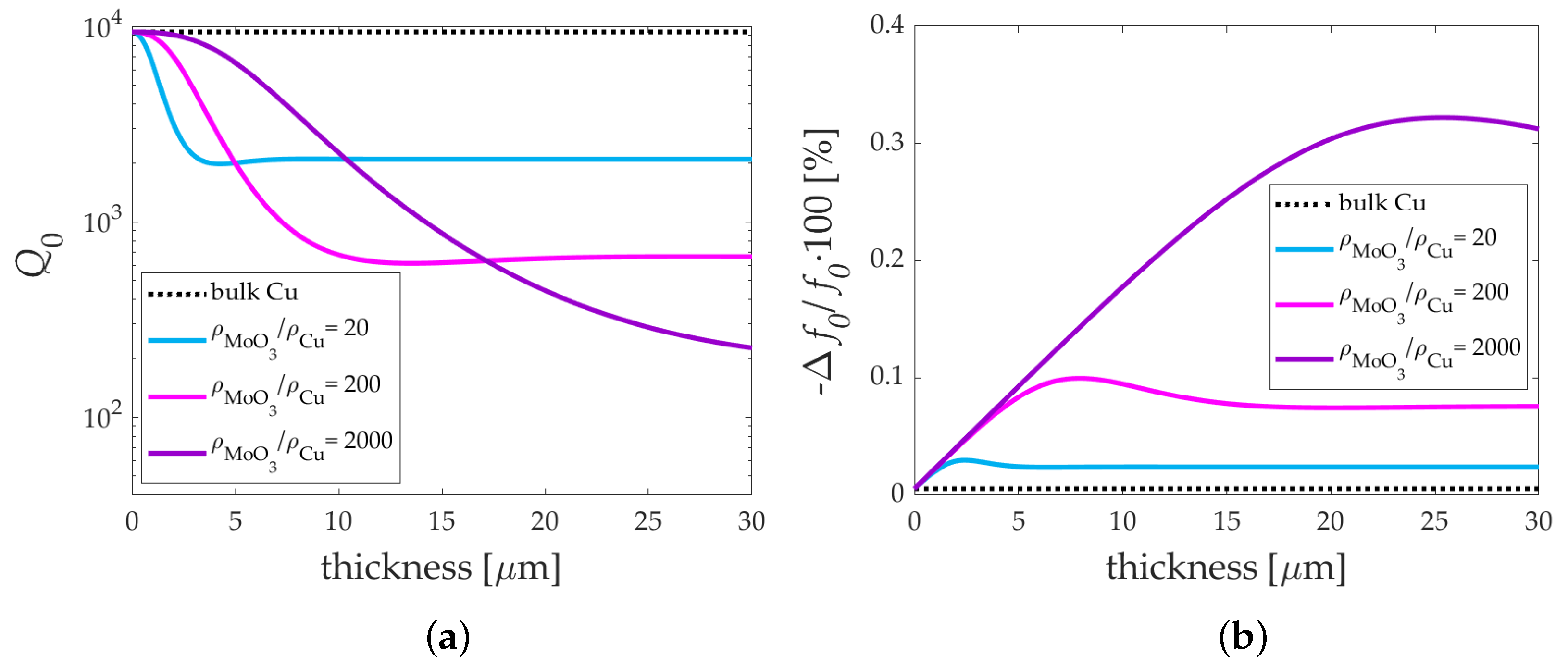
From the results shown in Figure 2 and Figure 3, the first important result of the study emerges: both Q 0 and Δ f of the film-layered cavity essentially behave as in the bulk case when the coating consists of a thin-film, as shown experimentally in Section 4. At the smallest thicknesses, Q 0 f 1 2 and Δ f f 1 2 , as bulk-Cu. However, perhaps counter-intuitively, the extra losses caused by the deposited film are slightly larger when the resistivity of finite-thickness conductive MoO 3 is closer to that of copper, while this effect does not appear when comparing Δ f . As a consequence, for a fixed thickness, a minimum Q 0 is reached at a finite layer conductivity, as shown in Figure 4. These observations can be explained by the fact that the film becomes electrically thinner at lower frequencies or greater resistivity. This latter feature also favors the mismatch at the film-substrate boundary so that impinging and reflected waves tend to cancel out each other. On the contrary, as the coating becomes thicker, Q 0 naturally degrades and Δ f increases, as shown in Figure 5 for the f 0 11.4 GHz case (in general, the quality factor degradation and frequency shifting are more noticeable at a higher frequency). As expected, in the bulk case the curves tend to saturate close to the bulk copper case as ρ MoO 3 / ρ Cu 1 . Notice that the Q 0 curves intersect due to the opposite arrangement in the thin-film and bulk cases. This occurs because highly resistive metal coatings in the thin-film regime yields the copper performance with good approximation.
Additionally, as a second important result of this work, it is worth stressing that both Q 0 and Δ f are not very sensitive to film properties, in terms of resistivity (defined as Q 0 / ρ MoO 3 and Δ f / ρ MoO 3 ; those derivatives are minor with respect to Q 0 and Δ f , respectively) and thickness (defined as Q 0 / t and Δ f / t ; those derivatives are minor with respect to Q 0 and Δ f , respectively). The Q 0 sensitivity decreases as the film is electrically thinner, whereas Δ f sensitivity is constant with film thickness and remains practically unchanged with frequency and MoO 3 resistivity (these features can be appreciated directly in Figure 2 and Figure 4 at the lowest thicknesses and largest resistivity ratios, respectively). This means that the cavity behavior would not be impacted by even relatively large inhomogeneities of the coating properties.
Finally, the validity of the model used throughout the analysis is checked in Figure 6. As the modulus of the effective impedance of the MoO 3 -film is in the same order of the one regarding the bulk-Cu surface impedance, it may be safely said that the perturbation is upon the same order at both frequency bands. As the bulk-Cu is well described by means of the first-order perturbation, the same holds for the layered structure with the MoO 3 -film.

4. Experimental Section

This section is intended to provide an experimental validation on the negligible influence of Mo oxide thin-films deposited on copper upon the cavity quality factor. It does not constitute, however, a demonstration of the full validity of the model, but a particular output in agreement with the results presented in Section 3. On the other hand, while the complete description of the measurement method, apparatus characteristics, and performances are thoroughly described in [24,25], here just the most significant aspects of the measurement procedure and the obtained results regarding the effective surface resistance ( R e f f ) of Mo thin-films are reported to support the potential use in accelerating cavities. As the goal of this measurement is to demonstrate that the R e f f of Mo oxide thin-film is indistinguishable from the R s of Cu, differential measurements ( Δ R s ) are carried out rather than the absolute ones, also in view of the reduced measurement uncertainty this non-calibrated method entails.
A Hakki–Coleman sapphire-loaded resonator equipped with an upper open window from which the sample under test is exposed to the excited mode (TE 011 ) is used, connected to an Anritsu 37269D Vector Network Analyzer (VNA). The employed resonator facilitates the sample mounting, so that the measurement repeatability is optimized. The measured samples are of ∼1 cm 2 of bulk copper (used as reference), and ∼50 nm and ∼100 nm of Mo oxide layers deposited on copper. Each sample is mounted n = 11 times. For each mounting, the transmission scattering parameters (measured at ∼5 the full-width half-maximum (FWHM) of the resonance centered at f 0 12.976 GHz , and sampling the frequency span with the maximum number of points (1601) available) are fitted by means of a Lorentzian curve, as shown in Figure 7, and described in [24] in detail. The fitting parameter under investigation is the loaded quality factor Q L , which essentially comprises the losses of each component of the resonator (since the port coupling is negligible in comparison with the resonator Q 0 ), including the sample under test.
The mean Q L ( Q ¯ L ) together with the measurement standard deviation ( σ Q L ) and the mean value uncertainty ( u ( Q ¯ L ) ) are reported in Table 2. From these results, it can be seen that (i) as Q ¯ L of the mounting with the bulk and that of the 100 nm Mo oxide coating are the same, it is already evident that those samples are indistinguishable in terms of R s ; and (ii) both the relatively low statistical deviation and measurement uncertainty point to the high repeatability and trueness of the experiment, respectively. Furthermore, and based on the high repeatability of the mounting, the differential measurements (with respect to copper) may be obtained once the sample geometrical factor ( G s 3380   Ω ) is computed. Those are also shown in Table 2. As seen through the obtained results, the differences on R s between the Mo oxide films and bulk Cu are below the measurement uncertainty (which is in the order ∼1 m Ω , as stated in [24]), and so the potential Q 0 of the coated accelerating cavity would be close to the bulk one. Reciprocally, the minimum ρ MoOx , m i n that fits the u ( Δ R ) in our model is reported in Table 2 (for 50 nm and 100 nm , taking ρ Cu = 1.67   μ Ω cm , as for the numerical analysis presented in Section 3). As the true resistivity of the film is expected to be always greater than those estimated minimums, the introduced model is further proved to be valid.

5. Conclusions

In this paper, the effects of MoO 3 coatings on the accelerating cavity parameters completely determining their linear RF response Q 0 and Δ f / f have been thoroughly studied. For this purpose, the classical expression describing the Z s of bulk conductors has been generalized to the case of normal conducting thin-film deposited on a metallic substrate. At the same time, the perturbation on the accelerating field introduced by the coating finite conductivity was rigorously evaluated. Then, Z e f f has been numerically checked for a couple of case studies at different frequency bands. In addition, experimental results are provided proving the negligible impact of Mo oxide coatings deposited on Cu in terms of R s , a result which is explained by this numerical analysis and the underlying model.
The computed results show (i) relatively little impact of ( 30 to 300 ) nm MoO 3 metallic coatings on both Q 0 and Δ f , and the magnitude of the accelerating cavity field, since Z e f f Z s , C u at various microwave frequencies. In addition, (ii) the coated cavity performs almost sensitiveless to thickness and resistivity variations within large ranges, making the cavity performance highly robust against coating inhomogeneities. As the negligible impact on the cavity parameters is a pre-condition for the subsequent coating deposition work, these results allow for MoO 3 as potential candidate to mitigate the BDR with origin in dark currents due to its intrinsically high WF.
As the analysis has been treated in a generalized way, and the respective parametrizations have been explored in a relatively large range, one can safely extrapolate these results to either molybdenum coatings made of different phases (e.g., molybdenum dioxide MoO 2 , or heterogeneous molybdenum metallic films [26]) or other conductive materials.

Author Contributions

Conceptualization, S.S. and B.S.; formal analysis, P.V.G. and N.P.; manuscript preparation, P.V.G. and N.P.; critical reading, S.S., M.C., L.G., A.M., B.S., A.A., K.T. and E.S.; supervision, S.S., B.S. and N.P.; funding acquisition, E.S. and N.P. All authors have read and agreed to the published version of the manuscript.

Funding

This research received no external funding.

Data Availability Statement

Data are provided in the figures and tables of the article. Data files are available upon request to the corresponding author.

Conflicts of Interest

The authors declare no conflict of interest.

Appendix A

The EM analysis regarding the modes of the accelerating cavity (TM modes) surrounded by film is tackled here. The “successive approximation scheme” (i.e., the perturbation analysis) presented in [21] for the bulk conductor is extended to the case in which the penetrating field is reflected at the film–substrate boundary (see Figure 1). The asymptotic expression of the field is thus obtained.
The accelerating field ( E z ) completely determines the EM fields of TM modes in the ideal cavity. At each cavity cross-section (see Figure A1), Φ 0 E z denotes the exact solution of the corresponding Dirichlet-2D-BVP:
2 Φ 0 + γ 2 Φ 0 = 0     ( Φ 0 = 0   on   S ) ;
where γ 2 = ( ω / c ) 2 k z 2 , and k z is the wave number along the perpendicular direction (e.g., k z = ± p π / L in cylindrical z-invariant coordinate systems, being L the cavity’s length).
Figure A1. Cross-section defining the BPV. The field penetrates normally to the contour ( S ), along which the EM field is continuous. The wave number k z ultimately defines the mode spectrum.
Instruments 07 00033 g0a1
The sought solution is hypothesized to be asymptotically equal to
Φ Φ 0 + ϵ Φ 1   ( ϵ 0 ) ,
where Φ 1 is the first-order correction. Φ 1 can be computed as a function of Φ 0 by imposing the continuity of the magnetic field at the boundary (see the notation used in Figure 1):
H t | S i z ^ × t Φ 0 | S ω μ 0 1 1 k z 2 c ω 2 = H | S H i | S 1 Γ e f f , with
Γ e f f = Z e f f Z s , MoO 3 Z e f f + Z s , MoO 3
the effective reflection coefficient at the boundary cavity-film. Furthermore, the incident field ( E i ) is obtained by means of the characteristic impedance (i.e., the surface impedance), which points to z ^ . Further continuity of the electric field leads to negative feedback to be added as perturbation to the accelerating field:
ϵ Φ 1 | S E i | S 1 + Γ e f f = Z s , MoO 3 H i | S 1 + Γ e f f .
By solving H i | S from Equation (A3) and substituting it in Equation (A5), and further using Γ e f f from Equation (A4), ϵ Φ 1 may be rewritten as:
ϵ Φ 1 | S = i Z e f f ( n ^ · Φ 0 ) | S ω μ 0 1 1 k z 2 c ω 2 .
In Equation (A6), the term Z e f f ultimately controls the definitive validity of Equation (A2).
In order to obtain Z e f f , Γ e f f is written as the transformation of the reflection coefficient [19] at the boundary film-substrate ( Γ b ):
Γ e f f = Γ b   e 2 i k MoO 3 t , with Γ b = Z s , Cu Z s , MoO 3 Z s , Cu + Z s , MoO 3 .
Then, Z e f f is solved by substituting Equation (A7) in Equation (A4), leading to the expression in Equation (3) used for the analysis.

References

  1. Sicking, E.; Ström, R. From precision physics to the energy frontier with the Compact Linear Collider. Nat. Phys. 2020, 16, 386–392. [Google Scholar] [CrossRef]
  2. Emma, P.; Akre, R.; Arthur, J.; Bionta, R.; Bostedt, C.; Bozek, J.; Brachmann, A.; Bucksbaum, P.; Coffee, R.; Decker, F.J.; et al. First lasing and operation of an ångstrom-wavelength free-electron laser. Nat. Photon. 2010, 4, 641–647. [Google Scholar] [CrossRef]
  3. Lindroth, E.; Calegari, F.; Young, L.; Harm, M.; Dudovich, N.; Berrah, N.; Smirnova, O. Challenges and opportunities in attosecond and XFEL science. Nat. Rev. Phys. 2019, 1, 107–111. [Google Scholar] [CrossRef]
  4. Wang, F.; Adolphsen, C.; Nantista, C. Performance limiting effects in X-band accelerators. Phys. Rev. ST Accel. Beams 2011, 14, 010401. [Google Scholar] [CrossRef]
  5. Cahill, A.D.; Rosenzweig, J.B.; Tantawi, S.G.; Weathersby, S. High gradient experiments with X-band cryogenic copper accelerating cavities. Phys. Rev. Accel. Beams 2018, 21, 102002. [Google Scholar] [CrossRef]
  6. Grudiev, A.; Calatroni, S.; Wuensch, W. New local field quantity describing the high gradient limit of accelerating structures. Phys. Rev. ST Accel. Beams 2009, 12, 102001. [Google Scholar] [CrossRef]
  7. Wuensch, W. High-Gradient Breakdown in Normal-Conducting RF cavities. In Proceedings of the 8th European Particle Accelerator Conference, Paris, France, 3–7 June 2002; p. 134. [Google Scholar]
  8. Nordlund, K.; Djurabekova, F. Defect model for the dependence of breakdown rate on external electric fields. Phys. Rev. ST Accel. Beams 2012, 15, 071002. [Google Scholar] [CrossRef]
  9. Rosenzweig, J.B.; Cahill, A.; Dolgashev, V.; Emma, C.; Fukasawa, A.; Li, R.; Limborg, C.; Maxson, J.; Musumeci, P.; Nause, A.; et al. Next generation high brightness electron beams from ultrahigh field cryogenic rf photocathode sources. Phys. Rev. Accel. Beams 2019, 22, 023403. [Google Scholar] [CrossRef]
  10. Wuensch, W.; Achard, C.; Dobert, S.; Braun, H.H.; Syratchev, I.; Taborelli, M.; Wilson, I. Demonstration of high-gradient acceleration. In Proceedings of the 2003 Particle Accelerator Conference, Portland, OR, USA, 12–16 May 2003; Volume 1, pp. 495–497. [Google Scholar] [CrossRef]
  11. Wuensch, W.; Grudiev, A.; Heikkinen, S.; Syratchev, I.; Taborelli, M.; Wilson, I.; Adolphsen, C.; Döbert, S. A High-Power Test of an X-Band Molybdenum-Iris Structure. In Proceedings of the 22nd International Linear Accelerator Conference, Lübeck, Germany, 16–20 August 2004; Available online: https://cds.cern.ch/record/790355 (accessed on 29 July 2023).
  12. Cahill, A.D.; Rosenzweig, V.A.; Dolgashev, V.A.; Li, Z.; Tantawi, S.G.; Weathersby, S. rf losses in high gradient cryogenic copper cavity. Phys. Rev. Accel. Beams 2018, 21, 061301. [Google Scholar] [CrossRef]
  13. Fowler, R.H.; Nordheim, L. Electron Emission in Intense Electric Fields. Proc. R. Soc. Lond. 1928, 119, 173–181. Available online: https://www.jstor.org/stable/95023 (accessed on 29 July 2023).
  14. Bini, S.; Spataro, B.; Marcelli, A.; Sarti, S.; Dolgashev, V.A.; Tantawi, S.; Yeremian, A.D.; Higashi, Y.; Grimaldi, M.G.; Romano, L.; et al. Molybdenum sputtering film characterization for high gradient accelerating structures. Chin. Phys. C 2013, 37, 097005. [Google Scholar] [CrossRef]
  15. Scifo, J.; Marcelli, A.; Spataro, B.; Hampai, D.; Dabagov, S.; Sarti, S.; Di Trolio, A.; Moscatelli, R.; Macis, S.; Faillace, L. Molybdenum Oxides Coatings for High Demanding Accelerator Components. Instruments 2019, 3, 61. [Google Scholar] [CrossRef]
  16. Macis, S.; Aramo, C.; Bonavolontà, C.; Cibin, G.; D’Elia, A.; Davoli, I.; De Lucia, M.; Lucci, M.; Lupi, S.; Miliucci, M.; et al. MoO3 films grown on polycrystalline Cu: Morphological, structural, and electronic properties. J. Vac. Sci. Technol. A 2019, 37, 021513. [Google Scholar] [CrossRef]
  17. Klein, N.; Chaloupka, H.; Mueller, G.; Orbach, S.; Piel, H.; Roas, B.; Schultz, L.; Klein, U.; Peiniger, M. The effective microwave surface impedance of high-Tc thin-films. J. Appl Phys. 1990, 67, 6940. [Google Scholar] [CrossRef]
  18. Erdélyi, A. Asymptotic Expansions; Dover Publications, Inc.: New York, NY, USA, 1956. [Google Scholar]
  19. Balanis, C.A. Advanced Engineering Electromagnetics, 1st ed.; John Wiley & Sons, Inc.: New York, NY, USA, 1989. [Google Scholar]
  20. Rosenzweig, J.B. Fundamentals of Beam Physics, online ed.; Oxford Academic: Oxford, UK, 2003. [Google Scholar] [CrossRef]
  21. Jackson, J.D. Classical Electrodynamics, 3rd ed.; John Wiley & Sons, Inc.: New York, NY, USA, 1999. [Google Scholar]
  22. Pompeo, N.; Torokhtii, K.; Silva, E. Surface impedance measurements in thin conducting films: Substrate and finite-thickness induced uncertainties. In Proceedings of the IEEE International Instrumentation and Measurement Technology Conference (I2MTC), Turin, Italy, 22–25 May 2017; pp. 1–5. [Google Scholar] [CrossRef]
  23. Spataro, B.; Behtouei, M.; Di Paolo, F.; Leggieri, A. A low-perveance electron gun for a high-efficiency Ka-band klystron. Eur. Phys. J. Plus 2022, 137, 769. [Google Scholar] [CrossRef]
  24. Alimenti, A.; Torokhtii, K.; Vidal García, P.; Pompeo, N.; Silva, E. Design and Test of a New Dielectric-Loaded Resonator for the Accurate Characterization of Conductive and Dielectric Materials. Sensors 2023, 23, 518. [Google Scholar] [CrossRef]
  25. Alimenti, A.; Pittella, E.; Torokhtii, K.; Pompeo, N.; Piuzzi, E.; Silva, E. A Dielectric Loaded Resonator for the Measurement of the Complex Permittivity of Dielectric Substrates. IEEE Trans. Instrum. Meas. 2023, 72, 6001009. [Google Scholar] [CrossRef]
  26. Marcelli, A.; Spataro, B.; Castorina, G.; Xu, W.; Sarti, S.; Monforte, F.; Cibin, G. Materials and Breakdown Phenomena: Heterogeneous Molybdenum Metallic Films. Condens. Matter 2017, 2, 18. [Google Scholar] [CrossRef]
Figure 1. Simplified scheme describing the EM fields that define (a) Z s in the bulk-Cu case and (b) Z e f f in the MoO 3 -film case, at the cavity’s cross section boundary ( S ). In both cases, E z | S (plotted in yellow) represents the perturbation field ( E z in TM cases).
Instruments 07 00033 g001
Figure 2. Pill-box parameters at f 0 11.4 GHz : Q 0 (a) and Δ f / f 0 (b), as a function of MoO 3 film thickness and parameterized by the ratio between the coating and substrate resistivities ( ρ MoO 3 / ρ Cu ).
Instruments 07 00033 g002
Figure 3. Pill-box parameters at f 0 = 36.0 GHz : Q 0 (a) and Δ f / f 0 (b), as a function of MoO 3 film thickness and parameterized by the ratio between the coating and substrate resistivities ( ρ MoO 3 / ρ Cu ).
Instruments 07 00033 g003
Figure 4. Pill-box parameters at f 0 11.4 GHz : (a) Q 0 and (b) Δ f / f 0 , as a function of the ratio between the coating and substrate resistivities ( ρ MoO 3 / ρ Cu ), and parameterized by the MoO 3 film thickness.
Instruments 07 00033 g004
Figure 5. Pill-box parameters at f 0 11.4 GHz : (a) Q 0 and (b) Δ f / f 0 , as a function of MoO 3 film thickness in the bulk scale, and parameterized by the ratio between the coating and substrate resistivities ( ρ MoO 3 / ρ Cu ).
Instruments 07 00033 g005
Figure 6. Ratio | Z e f f | / | Z s , Cu | that establishes the validity of the first-order perturbation ( ϵ 0 ) at (a) f 0 11.4 GHz and (b) f 0 = 36.0 GHz .
Instruments 07 00033 g006
Figure 7. Resonance of the transmission scattering parameter S 21 . The measurements are fitted by means of a Lorentzian curve, as described in [24].
Instruments 07 00033 g007
Table 1. Pill-box parameters regarding the case studies. L and R are the pill-box length and radius.
Case Study f 0 [GHz]G [ Ω ] L [mm]R [mm]
X-band (Cryo-Cu-SLAC-#2) [5]11.4294256.7713.1210.04Instruments 07 00033 i001
Ka-band (Compact Light XLS) [23]36.0256.774.1643.188
Table 2. Summary of the measurement parameters and the corresponding uncertainties regarding Cu bulk and Mo thin-film samples. For the differential measurement, the Cu samples is used as reference.
Sample Q ¯ L σ Q L u ( Q ¯ L ) Δ R [ m Ω ] u ( Δ R ) [ m Ω ] ρ MoOx , min [ μ Ω cm ]
Bulk Cu5178139---
50 nm MoOx-on-Cu517253−0.71.21.74
100 nm MoOx-on-Cu517812801.51.76
Disclaimer/Publisher’s Note: The statements, opinions and data contained in all publications are solely those of the individual author(s) and contributor(s) and not of MDPI and/or the editor(s). MDPI and/or the editor(s) disclaim responsibility for any injury to people or property resulting from any ideas, methods, instructions or products referred to in the content.

