
A Self-Powered VDJT AC–DC Conversion Circuit for Piezoelectric Energy Harvesting Systems

1
Faculty of Science and Engineering, Southern Cross University, Lismore, NSW 2480, Australia
2
Department of Research and Development, Electronics Engineer, MYRA Corporate, Wollongbar Industrial Area, Alstonville, NSW 2477, Australia
3
Department of Electronics and Control Engineering, National Institute of Technology, Niihama College, Ehime 792-0022, Japan
4
Faculty of Science and Engineering, Southern Cross University, Gold Coast, QLD 4225, Australia
*
Author to whom correspondence should be addressed.
Designs 2023, 7(4), 94; https://doi.org/10.3390/designs7040094
Submission received: 31 May 2023
/
Revised: 2 July 2023
/
Accepted: 13 July 2023
/
Published: 20 July 2023
(This article belongs to the Section Electrical Engineering Design)
Abstract
:A comprehensive model for micro-powered piezoelectric generator (PG), analysis of operation, and control of voltage doubler joule thief (VDJT) circuit to find the piezoelectric devices (PD’s) optimum functioning points are discussed in the present article. The proposed model demonstrates the power dependence of the PG on mechanical excitation, frequency, and acceleration, as well as outlines the load behaviour for optimal operation. The proposed VDJT circuit integrates the combination of voltage doubler (VD) and joule thief circuit, whereas the VD circuit works in Stage 1 for AC (alternating current)–DC (direct current) conversion, while a joule thief circuit works in Stage 2 for DC–DC conversion. The proposed circuit functions as an efficient power converter, which converts power from AC–DC and boosts the voltage from low to high without employing any additional electronic components and generating duty cycles. The electrical nature of the input (i.e., PD) of a VDJT circuit is in perfect arrangement with the investigated optimisation needs when using the proposed control circuit. The effectiveness of the proposed VDJT circuit is examined in terms of both simulation and experiment, and the results are presented. The proposed circuit’s performance was validated with available results of power electronics interfaces in the literature. The proposed circuit’s flexibility and controllability can be used for various applications, including mobile battery charging and power harvesting.
1. Introduction
A piezoelectric generator (PG) is a trending technology that transforms mechanical vibration/oscillation, which is freely and readily available in the atmosphere, into electrical power (EP), that is, alternating current/voltage (AC). The scientific world has increased its focus on piezoelectric energy harvesting (PEH) devices during the past decade. In practice, PGs are confined to low-power domains in the micro/milliwatt category caused by physically constrained features like internal capacitance and resistance [1,2,3,4]. They can withstand extremely high pressure but have minimal strain and make huge material quantities challenging to use [5,6,7,8,9]. In contrast, most anticipated excitations are generally in the range of 0.1 to 1 kHz and produce low voltage levels, whereas most electronic equipment requires 3 to 5 V dc. Yet, the primary purpose of the PEH process is to operate small-scale electronic devices, including tiny batteries, quartz clocks, and animal tracking [10,11,12,13].
It should be noted that the employed PG in the PEH process creates AC voltage due to oscillations from the atmosphere. However, direct current (DC) is requisite for most power electronic equipment. Consequently, the PEH process necessitates a power harvesting circuit (PHC) known as a rectifier circuit for the rectification (i.e., AC–DC conversion) to utilise the produced power effectively. The schematic diagram of the PEH system used in the current investigation is shown in Figure 1.
The easiest and most straightforward way to convert AC–DC is using a conventional full-bridge rectifier circuit (FBR) compromise of four diodes. Thus, due to its forward voltage across each diode, the output of the FBR circuit is low. Several single and dual-stage power harvesting interfaces have been proposed in the existing literature to overcome this issue [14,15,16,17]. The single-stage circuit is utilised for AC–DC conversion, whereas the dual-stage circuit is employed for conversion, namely AC–DC and DC–DC. Figure 2. depicts a flow chart of both single and dual-stage circuits. The easiest approach to converting AC to DC is with a single-stage H-Bridge rectifier (HBR) circuit [11,18,19,20] to address the forward voltage, Vf issues of conventional diodes in the FBR circuit. Nonetheless, the HBR circuit’s outcome, in terms of output voltage and power, was limited, and the design parameters were not appropriately defined.
A dual-stage HBR circuit was proposed by Edla et al. [21] to address the abovementioned output voltage and power limitations. The DSHBR circuit also boosts the low output voltage into a high output voltage. In addition, it satisfactorily charged a battery with ratings of 1.2 V dc and 4 mA. However, due to the complex conversion processes (AC–DC and DC–DC), the power losses in the DSHBR circuit were more than the supplied power. Moreover, the DSHBR circuit employed additional devices such as auxiliary integrated circuits (ICs), multiple capacitors, and Zener diodes, resulting in significant energy dissipation, expense, and complexity in design. The suggested DSHBR circuit’s yield was still inadequate, and this investigation did not give acceptable electrical performance for the optimisation approach.
Another approach by Shareef et al. [22,23] proposed a rectifier-less AD-DC conversion by utilizing the synchronous inductor method and cold start-up characteristic to obtain efficient performance (only 0.65 mV ac was required for harvesting output of 254 µW). This approach, however, was inefficient because it also employed additional components, such as three capacitors, one digital logic controller, a polarity detector, three PGs, and a millihenry spectrum of the inductor. As a result, device miniaturisation was adamant and had high power consumption.
Later, another approach by Edla et al. [24] proposed a single-stage rectifier-less boost converter circuit for harvesting power from high-frequency excitations. The designed single-stage rectifier-less boosts converter (SSRBC) circuit used a PG as an impedance source. It employed two split inductors and one filter capacitor to integrate boost and buck-boost techniques. The designed integrated SSRBC circuit configuration worked in both positive and negative half-cycles. In their designed topology, inductors were energised by being enveloped by the current generated by the PG through the transistors. This aided active rectification of ultra-low amplitude (i.e., input voltage <0.5 V ac). The proposed circuit converted an input voltage of 0.5 V ac that the PG generates to 5.1 V dc, which may help develop vibration-based power conversion circuits for limited power devices, including sensors, quartz timepieces, and portable chargers. However, this circuit was adamant due to the employed additional components, namely polarity detectors, logic gates, multiple inductors, switches, and transistors.
Another approach, namely the buck-boost converter circuit, was proposed by Elie et al. [25] to address the low output voltage and power challenges and achieve a high outcome. The proposed circuit included two stages (AC–DC and DC–DC), several capacitors, and a sensorless IC to activate the transistors, increasing power dissipation above an acceptable limit.
Khushboo and Azad reported the performance of synchronised power harvesting on inductors for triboelectric power generation [26]. The proposed methodology included a piezoelectric nanogenerator (PENG), a vertically moving arrangement of polytetrafluoroethylene, nylon, copper, and aluminium sheets. A convenient interface and series and parallel coordinated transistor harvesting on inductor (SSHI) circuits were used to examine and optimise the electrical performance of PENG’s electrical interface. The series SSHI circuit dramatically increased the power extracted from piezoelectric ceramic materials during walking. The proposed series-SSHI circuit generated an output dc voltage of 32.78 V and dc output power of 55.90 µW with capacitance and resistance of 1 µF and 25 MΩ. However, the proposed circuit comprised several diodes, inductors, and switches, which resulted in high power dissipation.
Another method for increasing electrical output is using a non-linear switching process by employing additional components, namely metal-oxide-semiconductor field-effect-transistor (MOSFETs), additional inductors, polarity detectors, logic gate ICs, additional DC power supply to activate the logic gate ICs, and comparators [4,27,28,29,30]. However, the proposed circuits employed several auxiliary components and large inductors, diodes, and transformers, making them unsuitable for use in the present examination, which intended to minimise the size of the power electronics circuit (PEC), device compactness and pricing.
Most of the literature from the abovementioned literature focused on improving the low AC voltage into high DC voltage by switching methods and employing additional components. However, no attempt has been made to minimise conventional diodes and boost or stabilise the output voltage without utilizing additional components.
Therefore, to overcome this shortcoming of traditional circuits, the authors employed a combination of conventional VD [31], and the joule thief circuits from the literature [25]. The advantages of the proposed circuit are explained here. By employing VD and Joule thief circuits combination, the proposed circuit minimises the forward voltage losses across the diodes in the AC–DC conversion process (i.e., eliminating two diodes). It then boosts the rectified voltage into high DC voltage without employing polarity detectors, additional capacitors, inductors, Zener diodes, logic gates, or auxiliary circuits. In addition, the proposed circuit requires no maintenance and possesses the feature of self-powering controllability.
It can be noticed that most of the switching components were eliminated in the proposed circuit, as summarised in Table 1. The components elimination process results in a device miniaturisation process and low power consumption.
The proposed circuit is anticipated to be efficient because of its capacity to minimise the stress between switches and inductors. In addition, it does not include any supplementary interfaces to reduce conversion losses and costs. Because the proposed circuit asserts a unique design and structure that does not use any effective control logic function, it is anticipated to lessen the requirements on the supplementary controlling interfaces while increasing the system’s total efficiency. It is expected to work for mobile battery charging and power harvesting implementations.
2. PG Internal Characteristics and Power Conversion Circuits
This part describes the PG’s internal circuit modeling and explanation of the VD circuit when exposed to excitation, followed by the proposed VDJT circuit.
2.1. PG Circuit Model
The PEH technology is comprised of three major components: the mechanical interface, the PEC, and the energy storage device. The PGs are frequently positioned on cantilever beams. When the PG is subjected to excitement, it can function as a current supply in parallel to the internal capacitance, CP, as depicted in Figure 3a. Alternately, it also can be considered as voltage in series with its internal capacitor, CP [5,24,34,35,36]. The internal characteristics of the PG in AC voltage (i.e., positive and negative cycles) are explained below and depicted in Figure 3b [5,8,9,11,37,38,39,40,41,42].
From Figure 3, it can be seen that the produced PG current, iac, due to mechanical excitation, is expected to charge and discharge its internal capacitor, CP, in both half cycles. While charging its CP, no output power (i.e., AC) is anticipated from the PG. This transition is also known as the non-harvesting period (NHP). When the CP is fully charged, the PG’s output power flows through its electrodes and rectifies through the PEC. This period is called the harvesting period (HP). NHP and HP occur in both positive and negative cycles. The intervals 1, 3 (i.e., t0–1, t2–3) and 2, 4 (i.e., t1–2, t3–4) represent NHP and HP, respectively. In other words, the PG’s output current flows through the electrodes and rectifies through the PEC.
2.2. VD Circuit
The traditional VD circuit operates in Stage 1 and in alternating modes since AC incorporates both cycles, positive and negative. The VD circuit’s diodes are on and off and retain rectified voltage, V dc, in the load capacitor, CL1.
The operating modes of the VD circuit are summarised below:
- Mode 1: Positive half cycle
Interval 1 (Period: NHP):
- -
- No output
- -
- D1: OFF
Interval 2 (Period: HP):
- -
- D1: ON
- -
- V ac = V dc (C1: Charged)
- Mode 2: Negative half cycle
Interval 3 (Period: NHP):
- -
- No output
- -
- D2: OFF
Interval 4 (Period: HP):
- -
- D2: ON
- -
- V ac = V dc (C2: Charged)
Then, each of the voltages across the capacitors, C1, and C2, are added up to give the total output voltage. As a result, the VD circuit’s output voltage is doubled and stored in the load capacitor, CL1. The VD circuit’s output power varies with rectified voltage [11,43], and the optimum power output occurs when [5,8,9,11,37,38,39,40,41,42]:
The rectified power output, PO (t), and the load capacitor, CL1, are related according to the following equation:
2.3. VDJT Circuit
The proposed VDJT circuit encompasses Stages 1 and 2 and has six operational modes and is shown in Figure 4. As the VDJT circuit is regarded as an extension of the VD circuit (i.e., Stage 1), the functioning of Modes 1 and 2 of the VD and VDJT circuits is anticipated to be identical. As a result, the operation of Modes 3 to 6 is solely covered in this section.
Mode 3: Primarily, the switch Q1 is OFF. When both cycles are complete in Modes 1–2, the current runs through the CL1 (positive terminal), primary winding (L1), resistor (R1), base-emitter (B-E), and CL1 (negative terminal). As a small current passes through the secondary winding (L2), the collector–emitter (C-E) becomes slightly conductive.
Mode 4: Since L1 and L2 are coupled in opposite directions, they induce the voltage in L2, i.e., positive, and turn the transistor on with a higher force. Because both L1 and L2 are coupled in opposing ways, both create magnetic fields.
Mode 5: In this mode, the voltage induced in the L1 makes the B-E terminal widely (Q1: ON). Consequently, more current runs through the C-E terminal. In another way, increasing the voltage in the L1 increases the current flow through the L2 and C-E.
Mode 6: In this mode, once the core is saturated, there is no more variation in a magnetic field. Therefore, the induced voltage in the L1 disappears (Q1: OFF), and the path between the C-E is in non-conduction mode. Subsequently, the current flows through the different paths through the diode, D1, charges the load capacitor, CL2, and powers the load resistor, RL1. Later, the same procedure is reverted to Mode 1.
Since this study mainly focused on the PEC, the obtained output power through the proposed circuit is an essential parameter for validating the effectiveness of the VDJT circuit versus the currently utilised circuits in the research. In other words, the proposed energy harvesting circuits’ primary function is to harvest the maximum power. As a result, the PG’s average input power, P ac, may be represented as [21,31]:
where V ac, iac, VP, IP are the mean and peak voltage and current; correspondingly, φ denotes the phase difference between PG’s voltage and current [31].
The accumulated output DC voltage through the VDJT circuit can be deemed constant due to using Modes 1 to 6. As a result, the VDJT’s output can be computed as the product of the output voltage across its load capacitor, CL2, and current through its load resistor, RL1 [31].
3. Simulation Results
The proposed circuit’s primary function is to be used in battery recharging and power harvesting applications. Thus, to validate the applicability of the proposed circuit, it is evaluated using two distinct power sources: ideal sinusoidal AC voltage and impedance source (i.e., PG). This can be considered an advantage since the proposed circuit can also be used with the ideal source (refer to Section 3). The proposed circuit’s effectiveness was also verified with an impedance source, namely PD (i.e., Section 4).
In the LTspice software, the ideal sinusoidal AC voltage is adopted and applied to the proposed circuit. In the experimentation, the sinusoidal source is substituted with a PG. When a sinusoidal AC signal is applied to the proposed VDJT circuit, the AC voltage rectifies into DC, and rectified voltage is stored in the load capacitor, CL1 (i.e., Modes 1 to 2). When the CL1 is sufficiently charged, the joule thief circuit process occurs, as explained in Modes 3 to 6. The applied sinusoidal current to the VD circuit (Mode 1); a stored rectified voltage in CL1 (Mode 2); the current enveloping process in the principal and secondary windings (Mode 3 to 4) energised L2 and CL2 as a result of switching transition (Mode 5). The stored output voltage (Mode 6), as a result of all modes 1 to 6, are all plotted inside the framework of Figure 5, Figure 6, Figure 7, Figure 8 and Figure 9, respectively.
It is worth emphasizing that the accumulated rectified voltage in CL1 is a VD circuit’s outcome, while the stored output voltage in CL2 is a VDJT circuit’s outcome. In addition, the VDJT circuit does not operate unless the VD completely charges the CL1.
4. Experimental Results
A conventional piezoelectric cantilever beam was fabricated from an aluminum beam (dimensions: 205 mm × 20 mm × 1 mm). One end was attached to an excitation/mechanical shaker (model: APS-113), and the other end carried two electromagnets functioning as a proof mass. A macrofibres composite (MFC) patch (M2814-P2, 37 × 17 × 0.180 mm: length, width, thickness, CP = 33.90 nF) was bonded towards the fixed end of the cantilever beam, where the maximum potential strain existed.
A sinusoidal signal was sent by a function generator (Agilent 33210A, Santa Clara, CA, USA) to a power amplifier (2706, B & K Agilent), which boosted the input before triggering the shaker. The shaker created electromechanical excitations based on input oscillation amplitude and frequency to stimulate the cantilever beam. An inductance detector is used to measure the acceleration of the base excitation beam. Therefore, as a result of excitations, the patched PG creates AC from stimulation, which is used as an input voltage to the VDJT circuit. Figure 10 depicts the suggested prototype model and breadboard execution. To verify the feasibility of the proposed circuit, the VDJT circuit was evaluated using two different test conditions.
In Tests 1 and 2, the AC derived from the PG via VDJT was studied by adjusting the circuit design. In Test 1, the VDJT was examined by varying input voltage (i.e., 5, 10, 15 V ac: ) at a constant frequency (i.e., 2, 5 Hz), whereas Test 2 was examined with constant voltage (i.e., 1 V ac) at different frequencies (i.e., 10, 15, 20, 25, 30 Hz). In both scenarios, the applied voltage to the proposed circuit was measured two times during the experimentation to ensure accuracy. However, little voltage fluctuations occurred during the experimentation due to the mechanical excitations and the tolerance levels are summarised above.
In Tests 1 and 2, the output voltage through the VDJT circuit was stored in a load capacitor for a low current flow at a set voltage level. The attained voltage is then collected by connecting each load capacitance in parallel with the load resistor. Then, the oscilloscope (TBS 1052B) was used to measure the output voltage across the load capacitor. Then, the output power was calculated using the product of the output voltage across the load capacitor and current through the load resistor. A multimeter (DT 4200) was also used to verify the output voltage across the load capacitor. All the testing scenarios that are investigated through the proposed circuit are shown in Table 2.
The output voltage and power through the VDJT circuit obtained from Test 1 are depicted in Figure 11a,b. The proposed circuit’s outcome is examined with varying input voltages of 5, 10, and 15 V ac and resistances from 10 to 70 kΩ.
4.1. Test 1: Varying Input Voltage at a Constant Frequency
Figure 11a displays that increasing the load resistances from 10 to 70 kΩ boosts the output voltage at a given frequency irrespective of the applied input voltage. It is also worth noting that the VDJT circuit yielded the maximum output voltage at a load resistance of 70 kΩ. In addition, the input voltage was higher than the Vf of the diodes in the Stage 1 circuit to obtain maximum functionality. The main reason for yielding high output voltage is explained below.
Firstly, an input voltage of 5 V ac was applied to the proposed circuit at 2 Hz. As shown in Table 2, when the input voltage was higher than Vf of the VDJT diodes (Stage 1), the AC voltage was rectified into DC voltage and retained in the load capacitor, CL1. After CL1 is fully charged, the switch, Q1, is activated, and Stage 2 operation begins. As a result, the accumulated current in CL1 flows in both windings, namely L1 and L2, whereas the weak current goes via the terminal called C-E. Since L1 and L2 are connected in reverse directions, the current induces a magnetic field in L1 and L2. The induced voltage in the L2 turned on the switch with a higher bias. This occurred as a result of a rapid switching process, namely ON and OFF. Once the core was saturated, there was no change in the magnetic field. Thus, the induced voltage in the primary winding disappeared.
Accordingly, the switch was turned OFF, and the stored L2′s magnetic field was transferred via D1 and gathered in the CL2. Here, the stored voltage in the CL1 (Stage 1) was represented by the rectified voltage, V dc, while the accumulated voltage in the CL2 was denoted by the output voltage, VO. Note that all the load resistors were connected in parallel with the CL2, and the outcome was taken using an oscilloscope.
Similarly, other input voltages, namely 10 and 15 V ac, were applied at the same frequency, and the output was taken, as shown in Figure 11a. When the output voltage was stored in CL2, the voltage across the terminals and the current through the load resistor RL2 was measured, and the calculated output power is depicted in Figure 11b. The proposed circuit generated the highest output voltage of around 14 VO and the highest output power of approximately 3000 µW when the input voltage was 15 V ac and the frequency was 2 Hz, as shown in Figure 11.
Similarly, at a frequency of 5 Hz, the same input voltages were applied to the proposed VDJT circuit, and the calculated output voltage and power is represented in Figure 12a,b.
Regardless of the applied voltage to the proposed circuit at a frequency of 5 Hz, the increasing output voltage and power trend are consistent, and the outcome is shown in Figure 12. Contrary to the output voltage, the inclination of output power against the load resistances is rather different.
It is worth mentioning that the main reason for causing higher output voltage and power in comparison with 2 Hz is the high frequency that was applied to PG. In other words, when the applied frequency increased, the current produced by the PG was high due to capacitive reactance. Therefore, the output power applied to the VDJT was also increased. Consequently, the output voltage and power were higher in the case of 5 Hz compared to 2 Hz. However, the trends in both cases, namely 2, 5 Hz with an input voltage of 5, 10, and 15 V ac, are similar.
Furthermore, the suggested VDJT circuit contains just two diodes, while the typical FBR circuit contains four. Therefore, the voltage drop across the two additional diodes has been decreased. As a consequence, the output voltage and power were augmented as well.
Further examination of Figure CL1–2 reveals that the excitation frequency significantly influences the proposed system’s effectiveness. The output voltage of the proposed circuit at both frequencies 2 and 5 Hz is shown in Figure 13.
Even though the applied input voltage was set to 5 V ac, the higher output voltage was attained at a high frequency [18]. The governing factors for the higher output through VDJT, when the frequency was higher, are as follows [41,42,43,44]:
- While the frequency incremented, PG generated more current due to a decrease in capacitive reactance.
- When the PG current was increased, its output power was also increased, resulting in higher output power of the VDJT circuit.
Analogously, the voltage and resistances utilised were used to compute the output power, shown in Figure 14, for both frequencies, i.e., 2 and 5 Hz. The proposed design has a maximum output power of 3000 µW at a frequency of 2 Hz with an input voltage of 15 V ac. Likewise, at a frequency of 5 Hz, the proposed circuit produced the maximum output power of 5500 µW.
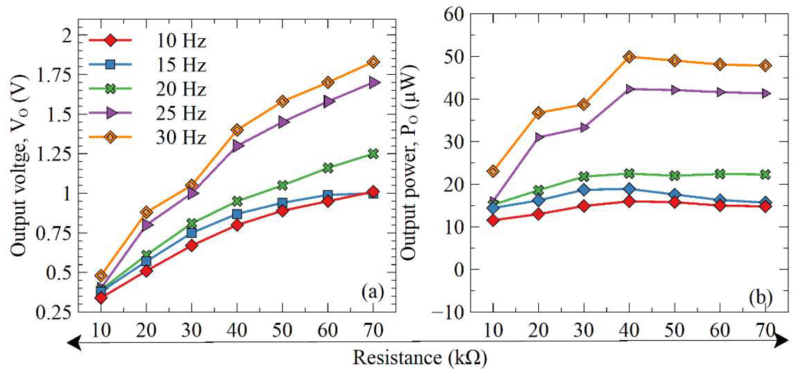
4.2. Test 2: Constant Input Voltage by Varying Frequencies
The performance of the developed circuit was also tested at various frequencies with keeping the applied input voltage constant at 1 V ac (at a frequency of 10 Hz). It should be noted that at each frequency, the input voltage was adjusted to 1 V ac. Figure 15 shows that independent of the frequency, the output voltage increases with the increase of the load resistance. The rise in output voltage, corresponding to Test 1, showed a consistent trend with the load resistance.
At first, 1 V ac input voltage was given to the VDJT circuit at 10 Hz. Since the produced voltage by the PG was greater than Vf, the output voltage and power through the VDJT circuit [25,45] were increased. Consequently, the load capacitor, CL2, stored the output voltage, and the recorded output voltage is shown in Figure 15.
It should be noted that similar to Test 1, the output voltage and power rose when the load resistance increased in the test settings. In summary, the proposed circuit generated the highest output voltage of 1.85 Vo and output power of 50 µW at a frequency of 30 Hz, as shown in Figure 15.
4.3. Comparison of VDJT Circuit with the Literature Circuits
It is evident that the proposed VDJT circuit consistently generated high output voltage and power in both Tests 1 and 2. To verify the effectiveness of the proposed circuit, its output was also compared with the recently published papers in the existing literature, as described in Table 3.
Generally, it is found that the VDJT circuit consistently delivered a significant output in comparison with the well-known buck-boost circuit and the circuits listed in the research. Furthermore, it is found in Table 3 that the suggested VDJT circuit outperforms various similar existing circuits in terms of production voltage and power.
5. Conclusions
This paper proposed and investigated a voltage doubler joule thief (VDJT) circuit to find the PG’s optimum points and output voltage and power dependence on varied vibration frequency and load resistances. To enhance the principles of VD and boost circuits, the VDJT circuit is proposed in this paper. It incorporates the well-known traditional voltage doubler circuit and the joule theory circuit in both Stages 1 and 2. The VDJT circuit was able to satisfy device miniaturisation standards and offer an efficient AC–DC conversion process without employing supplementary interfaces.
The applicability of the VDJT circuit was validated by simulation by employing the ideal AC source and laboratory testing by employing the impedance power source (i.e., PG). The VDJT circuit converted an input voltage of 15 V ac at a frequency of 5 Hz into an output voltage of 18 VO and power of 5500 µW, and at this instant, it is capable of delivering an efficiency of 72.3%. In conclusion, The VDJT circuit proved its functionality as an effective solution for the low output voltage and power from the traditional circuit. Although the proposed circuit converts low voltage into high voltage and boosts the low voltage into high voltage, the design of controlling methodology of boosting voltage in the Stage 2 process needs to be investigated.
Author Contributions
Conceptualization, M.K.; methodology, M.K. and M.E.; software, M.K. and M.E.; validation, M.K. and M.E.; formal analysis, M.K. and M.E.; investigation, M.K. and M.E.; resources, M.K., M.E. and A.M.T.; data curation, M.K., M.E. and A.M.T.; writing—original draft preparation, M.K. and M.E.; writing—review and editing, M.K., M.E. and A.M.T.; visualization, M.K., M.E., A.M.T., D.M. and V.B.; supervision, M.E., A.M.T. and D.M.; project administration, M.E., A.M.T. and D.M.; funding acquisition, M.E., A.M.T. and D.M.; All authors have read and agreed to the published version of the manuscript.
Funding
The study was supported by the “Southern Cross University”, Lismore, NSW, 2480, Australia.
Data Availability Statement
Data available on request.
Conflicts of Interest
The authors declare no conflict of interest.
References
- Erturk, A.; Inman, D.J. Piezoelectric Energy Harvesting; John Wiley & Sons: Hoboken, NJ, USA, 2011. [Google Scholar]
- Lefeuvre, E.; Badel, A.; Richard, C.; Guyomar, D. Piezoelectric energy harvesting device optimization by synchronous electric charge extraction. J. Intell. Mater. Syst. Struct. 2005, 16, 865–876. [Google Scholar] [CrossRef]
- Liu, H.; Zhong, J.; Lee, C.; Lee, S.-W.; Lin, L. A comprehensive review on piezoelectric energy harvesting technology: Materials, mechanisms, and applications. Appl. Phys. Rev. 2018, 5, 041306. [Google Scholar] [CrossRef] [Green Version]
- Lee, M.; Yang, J.; Park, M.; Jung, S.; Kim, J. Design and Analysis of Energy-Efficient Single-Pulse Piezoelectric Energy Harvester and Power Management IC for Battery-Free Wireless Remote Switch Applications. IEEE Trans. Circuits Syst. I Regul. Pap. 2018, 65, 366–379. [Google Scholar] [CrossRef]
- Edla, M.; Mikio, D.; Izadgoshasb, I.; Mahmud, M.P.; Kouzani, A.Z. Self-powered boost-converter for power optimisation and piezo garden lights. Smart Mater. Struct. 2022, 31, 045021. [Google Scholar] [CrossRef]
- Edla, M.; Lim, Y.Y.; Mikio, D.; Padilla, R.V. Non-Linear Switching Circuit for Active Voltage Rectification and Ripples Reduction of Piezoelectric Energy Harvesters. Energies 2022, 15, 709. [Google Scholar] [CrossRef]
- Muhammad, K.; Edla, M.; Thabet, A.M.; Haseeb, A.; Deguchi, M.; Bui, V. A Self-Powered AC-DC Conversion Circuit for Piezoelectric Energy Harvesting Systems. Energies 2023, 16, 1734. [Google Scholar] [CrossRef]
- Abdul, H.; Edla, M.; Ahmed Mostafa, T.; Deguchi, M.; Kamran, M. A Self-Powered Dual-Stage Boost Converter Circuit for Piezoelectric Energy Harvesting Systems. Energies 2023, 16, 2490. [Google Scholar]
- Abdul, H.; Edla, M.; Mustafa, U.; Fendy, S.; Deguchi, M. A Voltage Doubler Boost Converter Circuit for Piezoelectric Energy Harvesting Systems. Energies 2023, 16, 1631. [Google Scholar]
- Yuan, M.; Cao, Z.; Luo, J. Characterization the influences of diodes to piezoelectric energy harvester. Int. J. Smart Nano Mater. 2018, 9, 151–166. [Google Scholar] [CrossRef]
- Edla, M.; Lim, Y.Y.; Deguchi, M.; Padilla, R.V.; Izadgoshasb, I. An Improved Self-Powered H-Bridge Circuit for Voltage Rectification of Piezoelectric Energy Harvesting System. IEEE J. Electron Devices Soc. 2020, 8, 1050–1062. [Google Scholar] [CrossRef]
- Wen, N.; Fan, Z.; Yang, S.; Zhao, Y.; Cong, T.; Xu, S.; Zhang, H.; Wang, J.; Huang, H.; Li, C. Highly conductive, ultra-flexible and continuously processable PEDOT: PSS fibers with high thermoelectric properties for wearable energy harvesting. Nano Energy 2020, 78, 105361. [Google Scholar] [CrossRef]
- Naderipour, A.; Saboori, H.; Mehrjerdi, H.; Jadid, S.; Abdul-Malek, Z. Sustainable and reliable hybrid AC/DC microgrid planning considering technology choice of equipment. Sustain. Energy Grids Netw. 2020, 23, 100386. [Google Scholar] [CrossRef]
- Sedighi, M.; Padilla, R.V.; Alamdari, P.; Lake, M.; Rose, A.; Izadgoshasb, I.; Taylor, R.A. A novel high-temperature (>700 °C), volumetric receiver with a packed bed of transparent and absorbing spheres. Appl. Energy 2020, 264, 114705. [Google Scholar] [CrossRef]
- Shi, H.; Liu, Z.; Mei, X. Overview of Human Walking Induced Energy Harvesting Technologies and Its Possibility for Walking Robotics. Energies 2020, 13, 86. [Google Scholar] [CrossRef] [Green Version]
- Sharma, S.; Kiran, R.; Azad, P.; Vaish, R. A review of piezoelectric energy harvesting tiles: Available designs and future perspective. Energy Convers. Manag. 2022, 254, 115272. [Google Scholar] [CrossRef]
- Edla, M.; Lim, Y.Y.; Vasquez Padilla, R.; Deguchi, M. An Improved Rectifier Circuit for Piezoelectric Energy Harvesting from Human Motion. Appl. Sci. 2021, 11, 2008. [Google Scholar] [CrossRef]
- Arul, A.; Clarence, A.; Samuel, E.R. Efficiency Evaluation of a MOSFET bridge rectifier for Powering LEDs using Piezo-electric Energy Harvesting Systems. Automatika 2017, 57, 329–336. [Google Scholar]
- Maiorca, F.; Giusa, F.; Trigona, C.; Andò, B.; Bulsara, A.R.; Baglio, S. Diode-less mechanical H-bridge rectifier for “zero threshold” vibration energy harvesters. Sens. Actuators A Phys. 2013, 201, 246–253. [Google Scholar] [CrossRef]
- Edla, M.; Lim, Y.Y.; Padilla, R.V.; Mikio, D. Design and Application of a Self-Powered Dual-Stage Circuit for Piezoelectric Energy Harvesting Systems. IEEE Access 2021, 9, 86954–86965. [Google Scholar] [CrossRef]
- Salauddin, M.; Rana, S.S.; Sharifuzzaman, M.; Rahman, M.T.; Park, C.; Cho, H.; Maharjan, P.; Bhatta, T.; Park, J.Y. A Novel MXene/Ecoflex Nanocomposite-Coated Fabric as a Highly Negative and Stable Friction Layer for High-Output Triboelectric Nanogenerators. Adv. Energy Mater. 2021, 11, 2002832. [Google Scholar] [CrossRef]
- Shareef, A.; Goh, W.L.; Narasimalu, S.; Gao, Y. A rectifier-less ac–dc interface circuit for ambient energy harvesting from low-voltage piezoelectric transducer array. IEEE Trans. Power Electron. 2018, 34, 1446–1457. [Google Scholar] [CrossRef]
- Edla, M.; Lim, Y.Y.; Mikio, D.; Padilla, R.V. A Single-Stage Rectifier-Less Boost Converter Circuit for Piezoelectric Energy Harvesting Systems. IEEE Trans. Energy Convers. 2022, 37, 505–514. [Google Scholar] [CrossRef]
- Lefeuvre, E.; Audigier, D.; Richard, C.; Guyomar, D. Buck-Boost Converter for Sensorless Power Optimization of Piezoelectric Energy Harvester. IEEE Trans. Power Electron. 2007, 22, 2018–2025. [Google Scholar] [CrossRef]
- Azad, P. Design and analysis of a synchronized interface circuit for triboelectric energy harvesting. J. Electron. Mater. 2020, 49, 2491–2501. [Google Scholar]
- Eltamaly, A.M.; Addoweesh, K.E. A novel self-power SSHI circuit for piezoelectric energy harvester. IEEE Trans. Power Electron. 2017, 32, 7663–7673. [Google Scholar] [CrossRef]
- Lu, S.; Boussaid, F. A highly efficient P-SSHI rectifier for piezoelectric energy harvesting. IEEE Trans. Power Electron. 2015, 30, 5364–5369. [Google Scholar] [CrossRef] [Green Version]
- Dini, M.; Romani, A.; Filippi, M.; Tartagni, M. A nanopower synchronous charge extractor IC for low-voltage piezoelectric energy harvesting with residual charge inversion. IEEE Trans. Power Electron. 2015, 31, 1263–1274. [Google Scholar] [CrossRef]
- Xia, H.; Xia, Y.; Ye, Y.; Qian, L.; Shi, G.; Chen, R. Analysis and simulation of synchronous electric charge partial extraction technique for efficient piezoelectric energy harvesting. IEEE Sens. J. 2018, 18, 6235–6244. [Google Scholar] [CrossRef]
- Rashid, M.H. Power Electronics Handbook; Butterworth-Heinemann: Oxford, UK, 2017. [Google Scholar]
- Bimbhra, P.; Kaur, S. Power Electronics; Khanna Publishers: Delhi, India, 2012. [Google Scholar]
- Xia, H.; Xia, Y.; Shi, G.; Ye, Y.; Wang, X.; Chen, Z.; Jiang, Q. A Self-Powered S-SSHI and SECE Hybrid Rectifier for PE Energy Harvesters: Analysis and Experiment. IEEE Trans. Power Electron. 2020, 36, 1680–1692. [Google Scholar] [CrossRef]
- Tabesh, A.; Frechette, L.G. A Low-Power Stand-Alone Adaptive Circuit for Harvesting Energy From a Piezoelectric Micropower Generator. IEEE Trans. Ind. Electron. 2010, 57, 840–849. [Google Scholar] [CrossRef] [Green Version]
- Edla, M.; Lim, Y.Y.; Deguchi, M.; Padilla, R.V. A Novel Discontinuous Mode Piezoelectric Energy Harvesting Circuit for Low-Voltage Applications. In Proceedings of the 2021 31st Australasian Universities Power Engineering Conference (AUPEC), Perth, Australia, 26–30 September 2021; pp. 1–5. [Google Scholar]
- Yu, L.; Wang, H.; Khaligh, A. A discontinuous conduction mode single-stage step-up rectifier for low-voltage energy harvesting applications. IEEE Trans. Power Electron. 2016, 32, 6161–6169. [Google Scholar] [CrossRef]
- Ottman, G.K.; Hofmann, H.F.; Bhatt, A.C.; Lesieutre, G.A. Adaptive piezoelectric energy harvesting circuit for wireless remote power supply. IEEE Trans. Power Electron. 2002, 17, 669–676. [Google Scholar] [CrossRef] [Green Version]
- Chew, Z.J.; Zhu, M. Adaptive Maximum Power Point Finding Using Direct VOC/2 Tracking Method with Microwatt Power Consumption for Energy Harvesting. IEEE Trans. Power Electron. 2018, 33, 8164–8173. [Google Scholar] [CrossRef] [Green Version]
- Edla, M.; Deguchi, M.; Lim, Y.Y. A Self-Powered H-Bridge Joule Theory Circuit for Piezoelectric Energy Harvesting Systems. Power Electron. Devices Compon. 2022, 3, 100015. [Google Scholar] [CrossRef]
- Edla, M.; Lim, Y.Y. An Improved Piezoelectric Energy Harvesting Circuit for Reducing the Internal Loss. In Proceedings of the 83rd Researchfora International Conference, New Delhi, India, 29–30 January 2020. [Google Scholar]
- Edla, M.; Lim, Y.Y.; Mikio, D.; Ricardo Vasquez, P. Development of High-Efficiency Rectifier Circuits for Piezoelectric Energy Harvesting Systems. Ph.D. Thesis, Southern Cross University, Faculty of Science and Engineering, Lismore, Australia, 2022. [Google Scholar]
- Lee, H.-M.; Ghovanloo, M. An adaptive reconfigurable active voltage doubler/rectifier for extended-range inductive power transmission. IEEE Trans. Circuits Syst. II Express Briefs 2012, 59, 481–485. [Google Scholar]
- Chen, Y.; Wang, C.; Guo, J. A Highly Adaptive and Flipping-Time Optimized Piezoelectric Energy Harvesting Interface IC with Synchronized Triple Bias-Flip. IEEE Trans. Power Electron. 2022, 37, 14981–14992. [Google Scholar] [CrossRef]
- Gao, L.; Teng, L.; Fu, M.; Wang, H.; Liang, J. A Switched-mode Self-sensing Solution for Piezoelectric Synchronous Electric Charge Extraction (SECE). IEEE Trans. Ind. Electron. 2022, 70, 7457–7466. [Google Scholar] [CrossRef]
- Qi, N.; Dai, K.; Wang, X.; You, Z. Adaptive Capacitor Charging Circuit with Simplified Configuration for Efficient Piezoelectric Energy Harvesting. IEEE Trans. Power Electron. 2022, 37, 10267–10280. [Google Scholar] [CrossRef]
- De Pasquale, G.; Fraccarollo, F.; Somà, A. Performances evaluation of an autonomous sensing network node for rail vehicles supplied by a piezoelectric energy harvester. In Proceedings of the 10th International Workshop on Micro and Nanotechnology for Power Generation and Energy Conversion Applications, Leuven, Belgium, 30 November–3 December 2010; pp. 73–76. [Google Scholar]
- Liu, M.; Shen, H.; Luan, H. A new multi-piezoelectric input synchronized switch harvesting on inductor circuit. Ferroelectrics 2023, 606, 13–22. [Google Scholar] [CrossRef]
- Ben Ammar, M.; Sahnoun, S.; Fakhfakh, A.; Viehweger, C.; Kanoun, O. Self-Powered Synchronized Switching Interface Circuit for Piezoelectric Footstep Energy Harvesting. Sensors 2023, 23, 1830. [Google Scholar] [CrossRef]
- Zeng, W.; Shi, G.; Hu, X.; Shi, Z.; Pan, J.; Sun, Q.; Jia, S.; Han, J. A self-powered P–SSHI and boost hybrid interface circuit for Multi-PZTs and low voltage electromagnetic energy extraction. Microelectron. J. 2023, 135, 105745. [Google Scholar] [CrossRef]
- Mair, D.; Ferdik, M.; Happ, C.; Renzler, M.; Ussmueller, T. Numerical Optimization of a Fully Cross-Coupled Rectifier Circuit for Wireless Passive Ultra Low Power Sensor Nodes. Sensors 2019, 19, 4527. [Google Scholar] [CrossRef] [PubMed] [Green Version]
Figure 1.
Schematic diagram of the PEH process.

Figure 2.
Conversion processes, (a). Single (b). Dual stages.
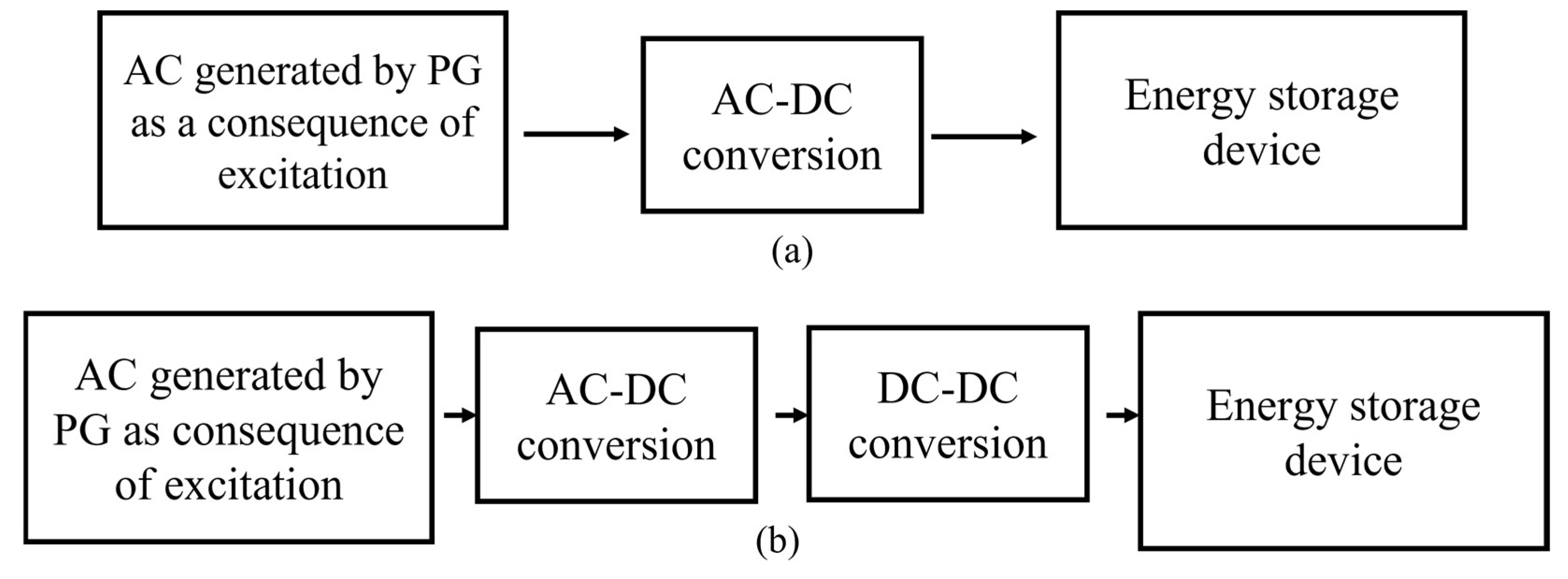
Figure 3.
PG and corresponding waveforms (a). PG depiction as a power supply and (b). PG output current and voltage.
Figure 3.
PG and corresponding waveforms (a). PG depiction as a power supply and (b). PG output current and voltage.
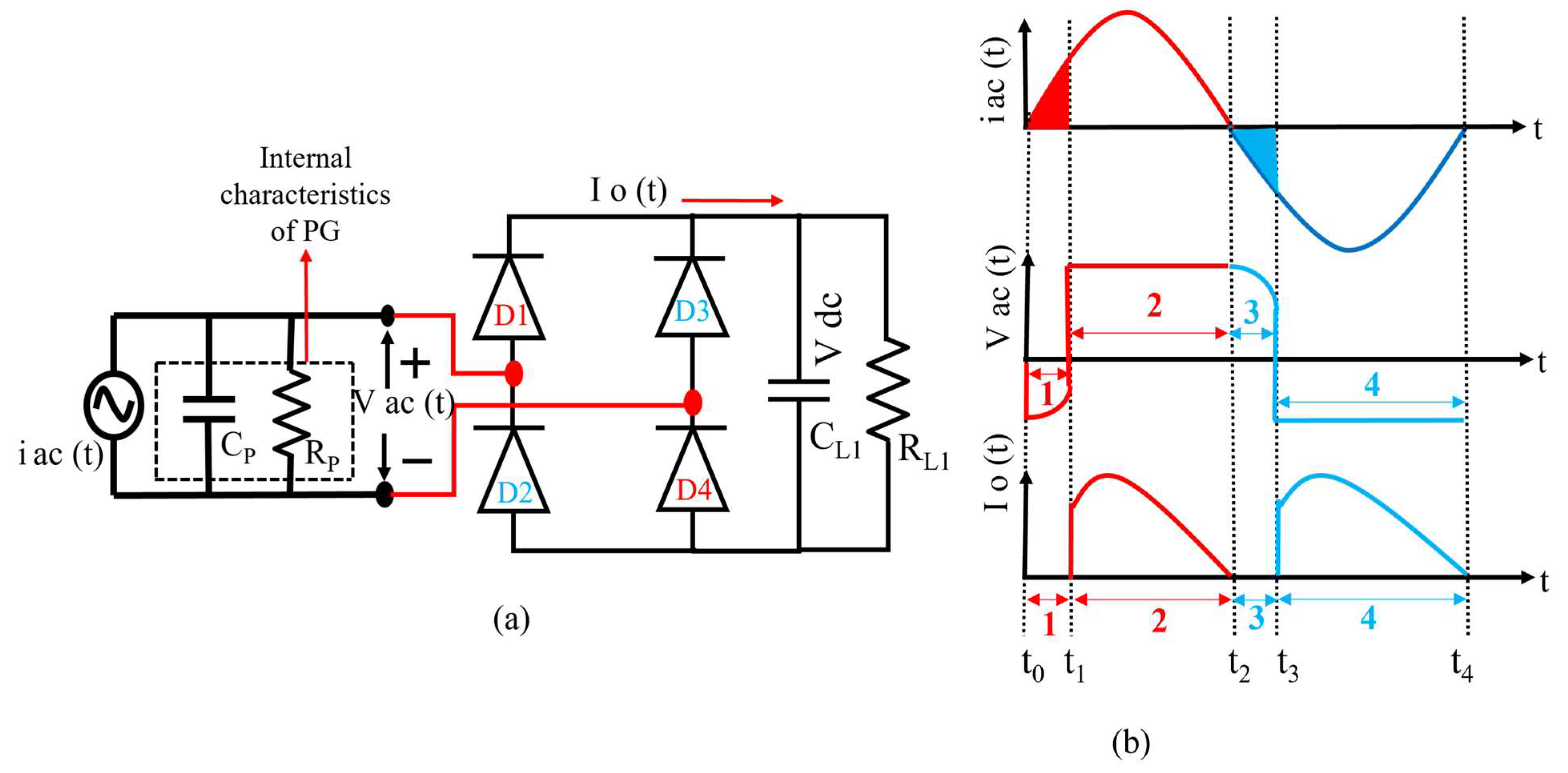
Figure 4.
The proposed VDJT circuit in Stage 1, 2, and conventional VD circuit in Stage 1 (parameter: C1–2: 0.27 µF, CL1: 47 µF, R1: 0.1 kΩ, L1–2: 47 µH).
Figure 4.
The proposed VDJT circuit in Stage 1, 2, and conventional VD circuit in Stage 1 (parameter: C1–2: 0.27 µF, CL1: 47 µF, R1: 0.1 kΩ, L1–2: 47 µH).

Figure 5.
Supplied ideal AC voltage to the proposed circuit.

Figure 6.
Stored rectified voltage in CL1.

Figure 7.
Energised windings (a). Principal and (b). Secondary.
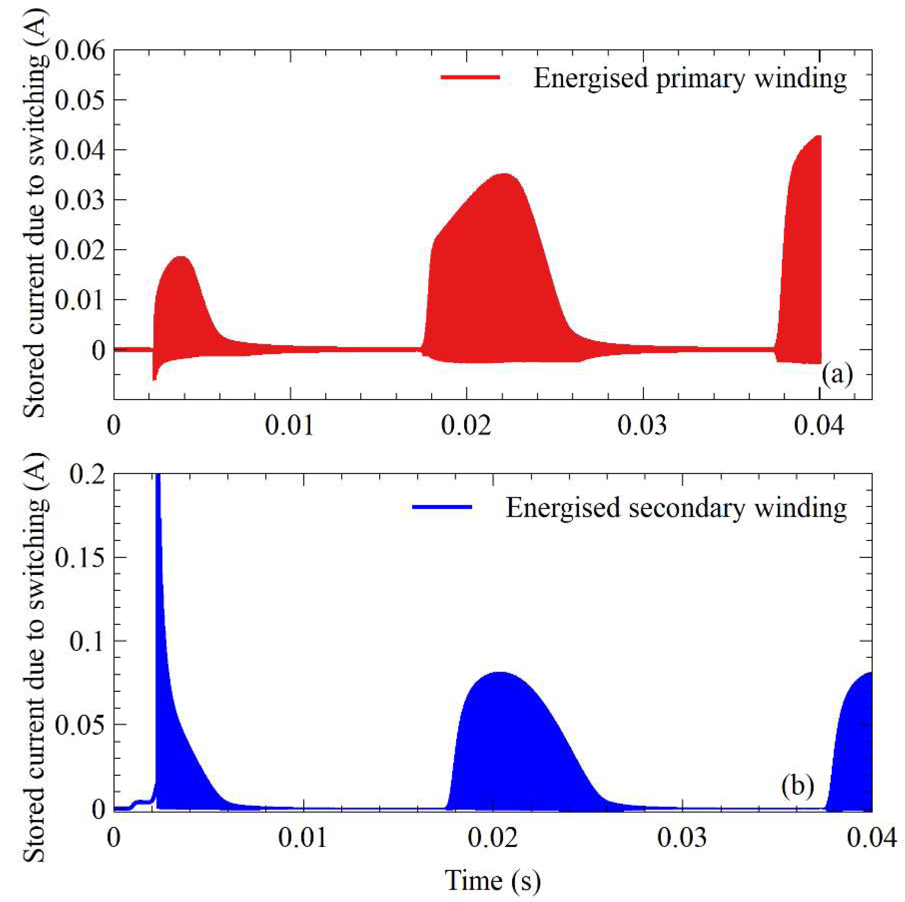
Figure 8.
Energising and charging procedures, (a). Zoom-in presentation of L2, (b). Charging procedure of load capacitor, CL2.
Figure 8.
Energising and charging procedures, (a). Zoom-in presentation of L2, (b). Charging procedure of load capacitor, CL2.

Figure 9.
Energising process of both load capacitors, (a). Stored rectified voltage in CL1, (b). Stored output voltage in the load capacitor, CL2, due to Modes 1–6.
Figure 9.
Energising process of both load capacitors, (a). Stored rectified voltage in CL1, (b). Stored output voltage in the load capacitor, CL2, due to Modes 1–6.

Figure 10.
Experimental circuit diagram and experimental setup.
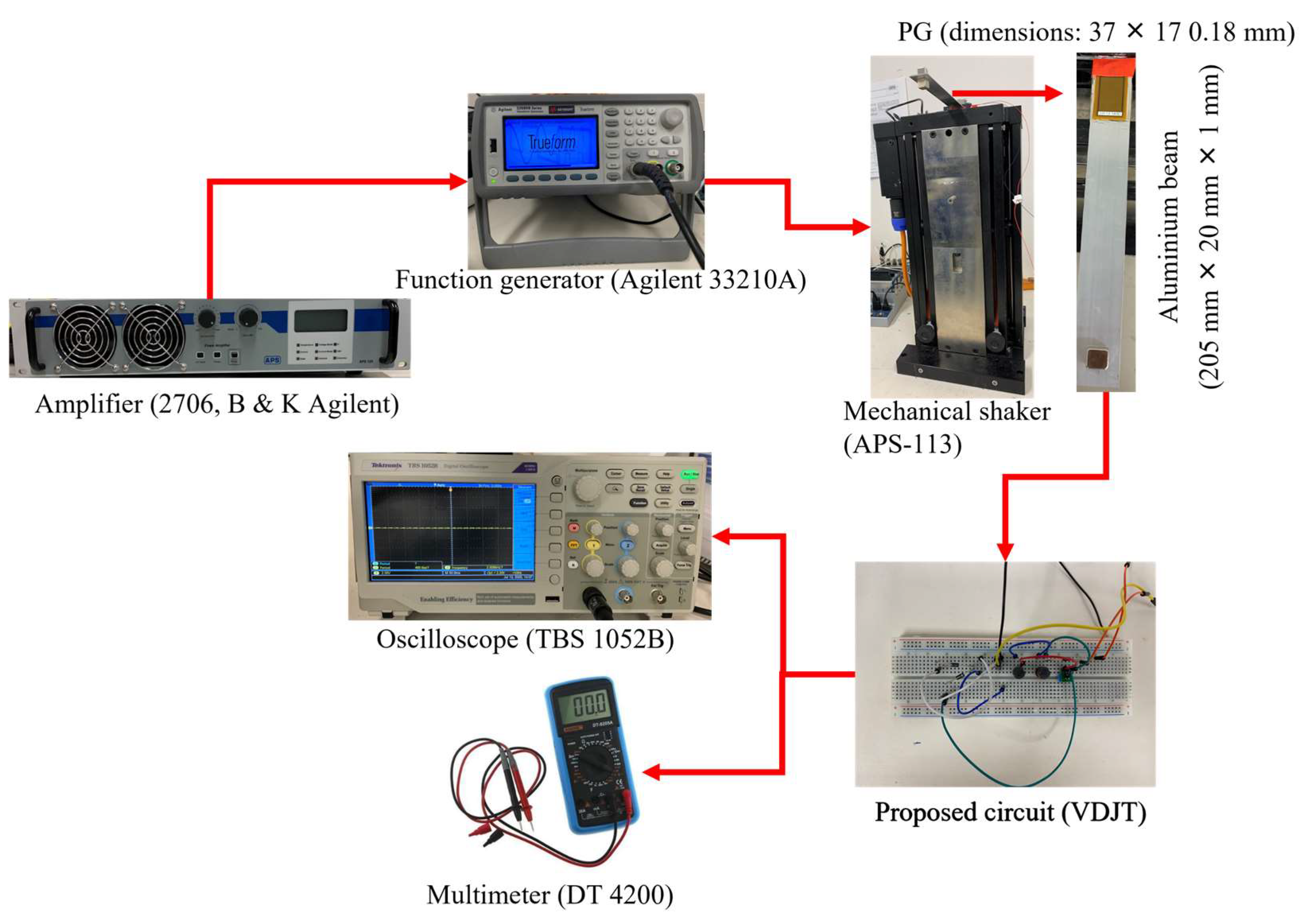
Figure 11.
Outcome of Test 1, (a,b). Output voltage and power.

Figure 12.
Outcome of Test 1 at various frequencies (a,b). Output voltage and power.
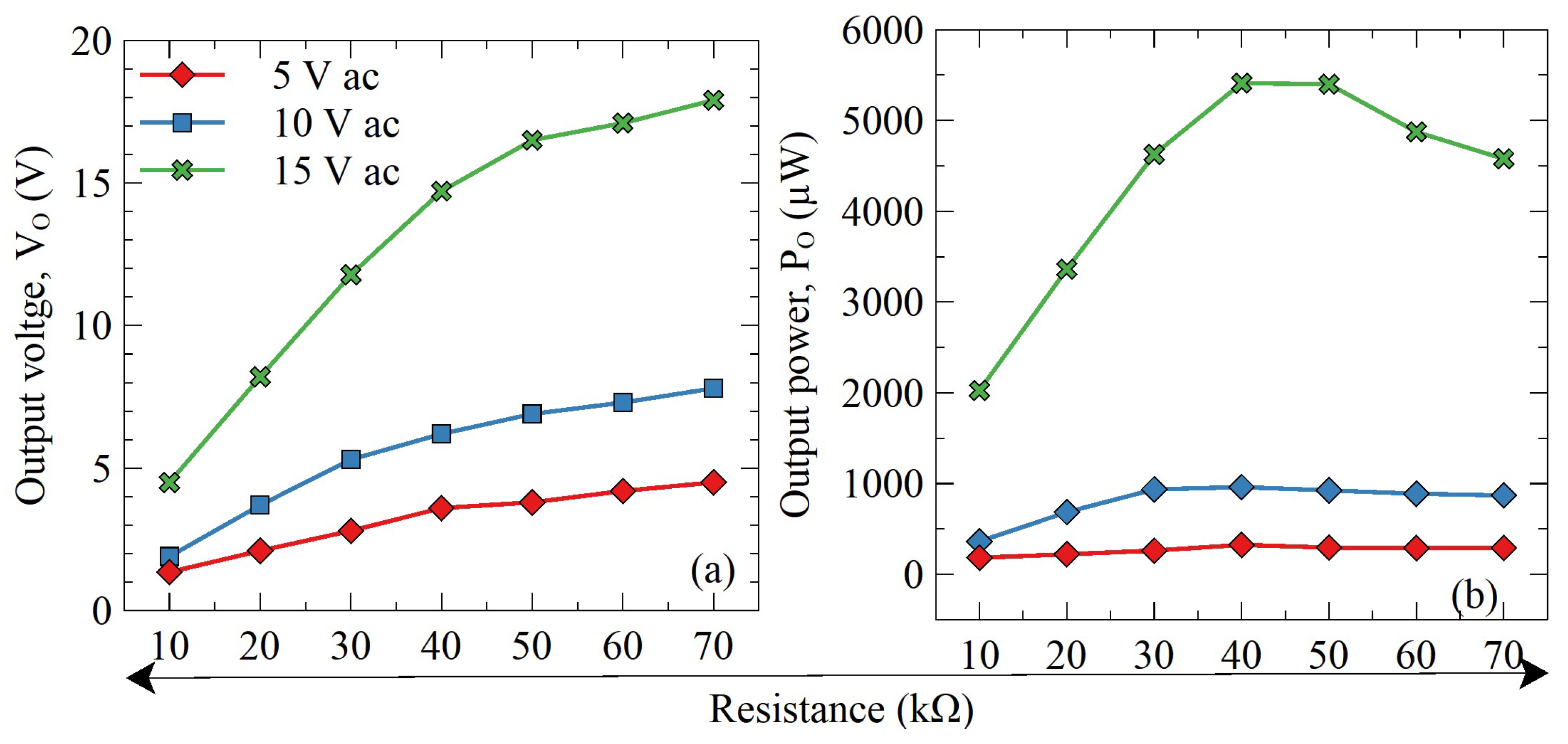
Figure 13.
Output voltage at different frequencies, (a). 2 Hz, (b). 5 Hz.
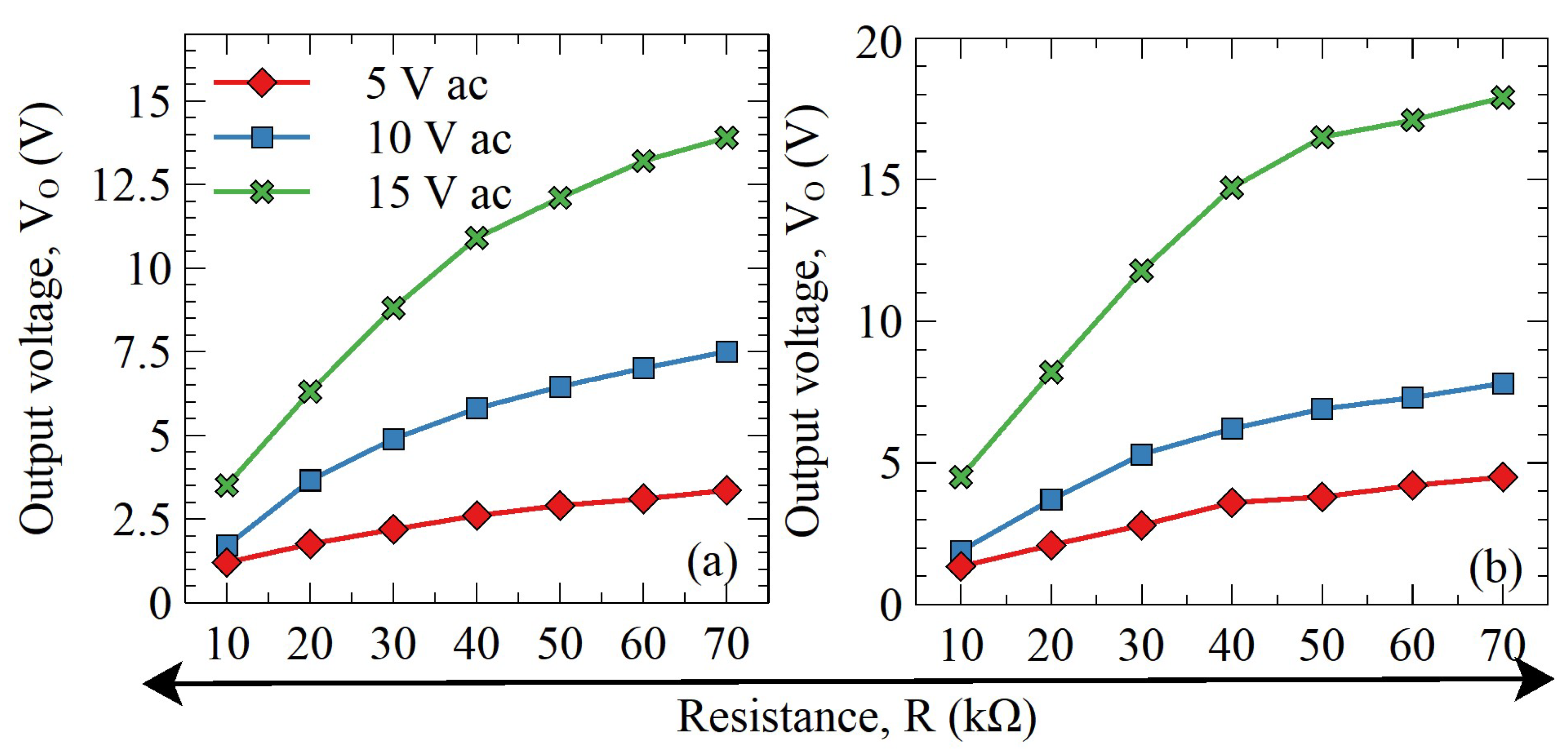
Figure 14.
Output power at different frequencies (a). 2 Hz, (b). 5 Hz.
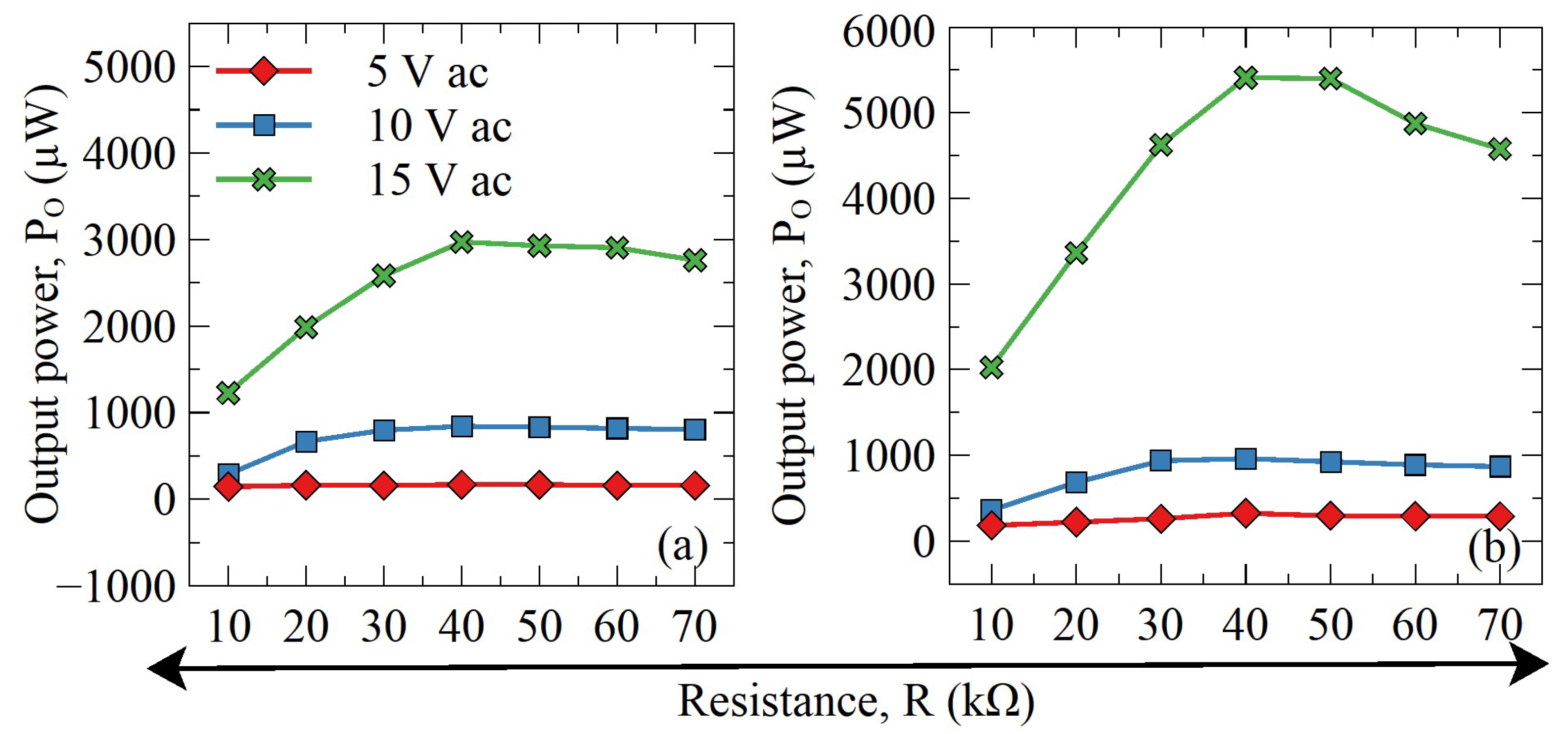
Figure 15.
Outcome of Test 2 through the VDJT circuit (a,b). Output voltage and power.

Table 1.
List components that are employed in the proposed circuit.
| Similar Circuits | Components–Quantity | |||||||
|---|---|---|---|---|---|---|---|---|
| Diodes | MOSFETs | Switch Drivers | Additional ICs | Inductors | Load Capacitors | Load Resistors | Auxiliary Circuits | |
| FBR [32] | 4 (0.67 Vf) | 0 | 0 | 0 | 0 | 1 | 1 | 0 |
| Dual-stage buck-boost converter [25] | 5 | 1 | 1 | 1 | 1 | 3 | 1 | 0 |
| SSRBC [24] | 3 | 4 | 2 | 0 | 2 | 1 | 1 | 1 |
| Hybrid rectifier [33] | 3 | 4 | 1 | 0 | 2 | 1 | 1 | 0 |
| Proposed VDJT | 2 | 1 | 0 | 0 | 2 | 1 | 1 | 0 |
Table 2.
Testing scenarios.
| Scenarios | Frequency (Hz) | Input Voltage V ac (V) | Load Capacitor (µF) | Load Resistor (kΩ) |
|---|---|---|---|---|
| Test 1 | 2, 5 | 5, 10, 15 | 10 | 10–70 |
| Test 2 | 10, 15, 20, 25, 30 | 1 |
Table 3.
Comparison of outcome of circuits in the literature.
| Literature Circuits | No. of PGs | Acceleration (g: m/s2) | Input Voltage (V) | Input Power (µW) | Output Power (µW) |
|---|---|---|---|---|---|
| [34] | 1 | - | 8 | 480 | 800 |
| [25] (similar circuit) | 1 | 1.5 | Frequency | 1100 | |
| 66 (resonance) | Not mentioned | ||||
| [7] (similar circuit) | 1 | 1.5 | 10 (not resonance) | 4901 | 3410 |
| [39] (similar circuit) | 1 | - | 3 | 676 | 520 |
| [46] | 1 | - | 10 | 900 | 195 |
| [47] | 1 | - | 8.6 | 238 | 167.2 |
| [48] | 1 | - | 4.2 | 2905 | 2000 |
| [49] | 1 | - | 1.5 | 10,756 | 6800 |
| [21] | 1 | - | 10 | - | 84.2 |
| [39] | 1 | - | 3 | - | 510 |
| VDJT | 1 | - | 15 | 7600 | 5500 |
Disclaimer/Publisher’s Note: The statements, opinions and data contained in all publications are solely those of the individual author(s) and contributor(s) and not of MDPI and/or the editor(s). MDPI and/or the editor(s) disclaim responsibility for any injury to people or property resulting from any ideas, methods, instructions or products referred to in the content. |
© 2023 by the authors. Licensee MDPI, Basel, Switzerland. This article is an open access article distributed under the terms and conditions of the Creative Commons Attribution (CC BY) license (https://creativecommons.org/licenses/by/4.0/).
Share and Cite
MDPI and ACS Style
Kamran, M.; Edla, M.; Thabet, A.M.; Mikio, D.; Bui, V. A Self-Powered VDJT AC–DC Conversion Circuit for Piezoelectric Energy Harvesting Systems. Designs 2023, 7, 94. https://doi.org/10.3390/designs7040094
AMA Style
Kamran M, Edla M, Thabet AM, Mikio D, Bui V. A Self-Powered VDJT AC–DC Conversion Circuit for Piezoelectric Energy Harvesting Systems. Designs. 2023; 7(4):94. https://doi.org/10.3390/designs7040094
Chicago/Turabian StyleKamran, Muhammad, Mahesh Edla, Ahmed Mostafa Thabet, Deguchi Mikio, and Vinh Bui. 2023. "A Self-Powered VDJT AC–DC Conversion Circuit for Piezoelectric Energy Harvesting Systems" Designs 7, no. 4: 94. https://doi.org/10.3390/designs7040094