Driving and Sensing M/NEMS Flexural Vibration Using Dielectric Transduction †

Laboratory for Analysis and Architecture of Systems (LAAS-CNRS), Université de Toulouse, CNRS, 7 Avenue du Colonel Roche, F-31400 Toulouse, France
*
Author to whom correspondence should be addressed.
†
Presented at the Eurosensors 2017 Conference, Paris, France, 3–6 September 2017.
Proceedings 2017, 1(4), 300; https://doi.org/10.3390/proceedings1040300
Published: 25 August 2017
(This article belongs to the Proceedings of Proceedings of Eurosensors 2017, Paris, France, 3–6 September 2017)
Abstract
:We show that nanometer-scale dielectric thin films can act as efficient electromechanical transducers to simultaneously drive and sense the vibration of the first flexural mode of micro/nano-cantilevers. Here, 16 μm-long, 5 μm-wide and 350 nm-thick cantilevers are actuated by a 15 nm-thick silicon nitride layer, and electrically detected by charge measurement at megahertz frequencies. The displacement was also checked by optical interferometry, and the electromechanical transduction efficiency is extracted and compared to an analytical modelling.
1. Introduction
NEMS devices offer great opportunities for applications in metrology and fundamental science, particularly when used as resonators [1]. However as the size is reduced, devices face the challenge of the efficiency of the electromechanical transduction. Capacitive and piezoelectric principles are commonly used in MEMS devices for both actuation and detection. At nanometer scale, issues are met. For example, piezoelectric actuation is dramatically impacted when the layer thickness is reduced under 100 nm, leading to a decrease in efficiency by orders of magnitude compared to the one expected from the bulk piezoelectric properties [2]. Besides, capacitive transduction strongly depends on the airgap width and a trade-off has to be made between efficiency and risk of failure due to stiction resulting from narrow air gaps. Conversely, high-K materials made for example by Atomic Layer Deposition (ALD) techniques are available in very thin films (<10 nm) and with a high quality. Such materials are compatible with silicon microtechnologies fabrication processes and make dielectric transduction a promising alternative for sensing and driving displacements at nanoscale. Actuation and detection have first been reported separately on cantilevers at a millimeter scale [3]. Recently, actuation has also been observed for micrometer scale devices [4]. Here, we report the simultaneous actuation and detection of MEMS/NEMS cantilever devices using high-K thin films as the electromechanical transducer.
2. Materials and Methods
In the present study, we used a 15 nm-thick low-stress silicon nitride film as the dielectric active layer. Its dielectric constant εd is about 8 and its Poisson’s ratio υd is 0.23. It was deposited using low-pressure chemical vapor deposition (LPCVD) on a doped silicon-on-insulator wafer etched beforehand to create air bridges along the signal paths to reduce extra parasitic capacitances to ground. A 20 nm-thick chromium layer was used as a top electrode. The 5 μm-wide and 16 μm-long cantilevers were patterned from this stack using chemical and reactive ion etchings and released by chemical etching of the buried oxide.
We perform actuation of the device using a bias voltage VDC added to an alternative signal VAC applied to the chromium electrode, across the dielectric thin film. Frequency of the alternative signal varies close to the fundamental mode resonance frequency. Simultaneously, we use differential excitation (−VAC) of a reference cantilever to subtract from the signal the parasitic coupling due to the cantilever static capacitance. Resulting motional charges are then detected and amplified with a 10 V/pC gain and the resulting signal is processed using a network analyzer. To validate the charge detection, we also measure the resonance frequency by Fabry-Perot interferometry: a laser beam is reflected both by the vibrating resonator and the substrate. The resulting interferometry signal is modulated by the vibration, and detected by a photodiode for frequency response analysis. All the measurements are made at room temperature and under vacuum (P = 2.10−1 mBar). Schematic cross-section, example of a fabricated device and measurement set-up are shown in Figure 1.
3. Results
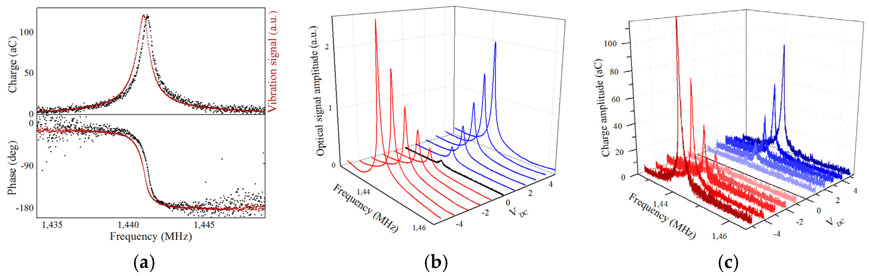
The 5 μm × 16 μm device is tested applying a 600 mV VAC signal and a VDC bias ranging from −5 to 5 V. Optical and capacitive measurements have similar features: a 1.441 MHz resonance frequency, and a quality factor Q of 2200. Figure 2 shows an example of capacitive and optical amplitude and phase measurements for VDC = −5 V (a), and optical (b) and capacitive (c) amplitude frequency responses in magnitude versus VDC.
4. Discussion
The dielectric actuation exploits electrostatic pressure on the dielectric film, which depends on the square of the voltage applied across the film. As we use a superposition of VDC and VAC, we expect the vibration amplitude at resonance frequency to be linear with VDC. Similarly, as the electrical detection principle is based on the variation of charges in the capacitor formed by the device, the detected charge is proportional to the VDC bias. Consequently, during simultaneous actuation and detection, the measured charge variation has a parabolic dependence versus the bias. The Figure 3 shows the optical and charge measurements fitted with linear and parabolic functions respectively.
For VDC = −5 V and VAC = 600 mV, and taking into account the oxide over etching, the expected variation of charge is 195 aCI as calculated by an analytical approach inspired from Reference [5]:
where the thickness and width of the cantilever are respectively e = 320 nm and w = 5 µm, and the thickness, Poisson ratio, and dielectric coefficient of the silicon nitride layer are t = 15 nm, υd = 0.23, and εd ≈ 8 respectively.
The measured charge for these driving conditions is 125 ± 25 aC, which is slightly lower than the theoretical value. From this measurement, and using a calibration of the optical set-up based on the thermomechanical noise method, we can calculate the transduction efficiency of the device, defined as the ratio between the beam displacement and its charge: 𝜂 = 361 ± 70 pN/V. Again, the result is comparable to the theoretical value, 452 pN/V, obtained using the Reference [5] approach:
The 20% difference between the two values can be explained by measurements uncertainties and by the fact that the chromium electrode does not cover exactly the whole cantilever surface.
Table 1 summarizes the results and the main parameters of the cantilever device and its dielectric transducer.
5. Conclusions
To conclude, simultaneous dielectric actuation and detection were successfully demonstrated for flexural devices with a nanometer scale active layer thickness. Results are in a good agreement with theoretical calculations, including the transduction efficiency. Using high-K thin-film materials with higher dielectric constants such as Al2O3 (εd = 9) and HfO2 (εd = 20) would be a promising way to achieve efficient actuation and detection with even greater efficiencies. Such devices are currently under fabrication and will be presented in a later study.
Acknowledgments
We acknowledge the French technological Network RENATECH and in particular the LAAS clean room staff for its constant support.
Conflicts of Interest
The authors declare no conflict of interest.
References
- Schmid, S.; Villanueva, L.G.; Roukes, M.L. Fundamentals of Nanomechanical Resonators; Springer International Publishing: Cham, Switzerland, 2016. [Google Scholar]
- Dezest, D.; Thomas, O.; Mathieu, F.; Mazenq, L.; Soyer, C.; Costecalde, J.; Remiens, D.; Deü, J.F.; Nicu, L. Wafer-scale fabrication of self-actuated piezoelectric nanoelectromechanical resonators based on lead zirconate titanate (PZT). J. Micromech. Microeng. 2015, 25, 035002. [Google Scholar] [CrossRef]
- Bouwstra, S.; Blom, F.R.; Lammerink, T.S.J.; Yntema, H.; Schrap, P.; Fluitman, J.H.J.; Elwenspoek, M. Excitation and detection of vibrations of micromechanical structures using a dielectric thin film. Sens. Actuators 1989, 17, 219–223. [Google Scholar] [CrossRef]
- Fuinel, C.; Daffé, K.; Laborde, A.; Thomas, O.; Mazenq, L.; Nicu, L.; Leichlé, T.; Legrand, B. High-K thin films as dielectric transducers for flexural M/NEMS resonators. In Proceedings of the 29th IEEE Conference on Micro Electro Mechanical Systems, MEMS 2016, Shanghai, China, 24–28 January 2016; pp. 1193–1196. [Google Scholar]
- DeVoe, D.L. Piezoelectric thin film micromechanical beam resonators. Sens. Actuators A 2001, 88, 263–272. [Google Scholar] [CrossRef]
Figure 1.
(a) Schematic cross-section (top) and top view (bottom) of a micro-cantilever; (b) Scanning electron microscope image of a fabricated device. A denotes the cantilever, B its anchor area connected to the charge amplifier, C the gold signal line, D the air bridge. Inset: close view of the junction of the cantilever with its anchor where 1 indicates the silicon structural layer, 2 the silicon nitride layer and 3 the chromium layer; (c) Optical and electrical measurement set-up of the device resonance frequency response.

Figure 2.
(a) Charge (black dots) and optical (red dots) measurements of the cantilever device resonance versus frequency when driven by VDC = −5 V and VAC = 600 mV applied to the chromium top electrode; (b) Measurement by optical interferometry of the magnitude signal close to resonance for VDC values ranging from −5 to +5 V; (c) Charge magnitude measurement close to resonance for VDC values ranging from −5 to +5 V. The charge curves were obtained by averaging 6 measurements.

Figure 3.
Fitted measurements of the vibration signals at resonance versus VDC. Optical measurements (a) were made for VAC = 140 mV and capacitive measurements (b) for VAC = 600 mV.
Figure 3.
Fitted measurements of the vibration signals at resonance versus VDC. Optical measurements (a) were made for VAC = 140 mV and capacitive measurements (b) for VAC = 600 mV.


Table 1.
Summary of the device and dielectric transducer parameters.
| Cantilever Parameters | Transducer Parameters | ||
|---|---|---|---|
| Length | 16 µm | Material | Si nitride |
| Width | 5 µm | Thickness | 15 nm |
| Si thickness | 320 nm | Permittivity | εd ≈ 8 |
| Eff. stiffness | 1.38 N/m | Transducer efficiency theoret. | 452 pN/V at VDC = −5 V |
| fres analytic. | 1.45 MHz | ||
| fres experim. | 1.441 MHz | Transducer efficiency exp. | 361 pN/V at VDC = −5 V |
| Q factor | 2200 | ||
| Qm theror. Charge at VDC = −5 V, VAC = 600 mV | 195 aC | ||
| Qm exp.charge at VDC =−5 V, VAC = 600 mV | 125 aC | ||
© 2017 by the authors. Licensee MDPI, Basel, Switzerland. This article is an open access article distributed under the terms and conditions of the Creative Commons Attribution (CC BY) license (https://creativecommons.org/licenses/by/4.0/).
Share and Cite
MDPI and ACS Style
Fuinel, C.; Mathieu, F.; Legrand, B. Driving and Sensing M/NEMS Flexural Vibration Using Dielectric Transduction. Proceedings 2017, 1, 300. https://doi.org/10.3390/proceedings1040300
AMA Style
Fuinel C, Mathieu F, Legrand B. Driving and Sensing M/NEMS Flexural Vibration Using Dielectric Transduction. Proceedings. 2017; 1(4):300. https://doi.org/10.3390/proceedings1040300
Chicago/Turabian StyleFuinel, Cécile, Fabrice Mathieu, and Bernard Legrand. 2017. "Driving and Sensing M/NEMS Flexural Vibration Using Dielectric Transduction" Proceedings 1, no. 4: 300. https://doi.org/10.3390/proceedings1040300