Transparent Glass/SU8-Based Microfluidic Device with on-Channel Electrical Sensors †


Department of Microsystems Engineering (IMTEK), University of Freiburg, 79110 Freiburg im Breisgau, Germany
*
Author to whom correspondence should be addressed.
†
Presented at the Eurosensors 2017 Conference, Paris, France, 3–6 September 2017.
Proceedings 2017, 1(4), 336; https://doi.org/10.3390/proceedings1040336
Published: 17 August 2017
(This article belongs to the Proceedings of Proceedings of Eurosensors 2017, Paris, France, 3–6 September 2017)
Abstract
:This paper presents a transparent microfluidic chip designed for continuous-flow photochemistry applications with integrated electrical sensing. The transparent chip design allows for microscale photochemistry, and permits direct, real-time visual/electrical observation. The microchip uses optically transparent indium tin oxide (ITO) electrodes for reagent and phase tracking. High-speed videography was performed to validate the electrical measurement data.
1. Introduction
The use of integrated electrical sensors for microfluidic chips has received ever greater attention recently, since visual inspection is not always quantitatively sufficient for process characterization [1]. Several groups in the last decade have demonstrated new designs in the field of analytical microfluidics. PDMS/glass systems are the most common substrates for such “Lab-on-a-Chip” platforms, however they are not suited for many applications with harsh chemical or thermal conditions [2]. In this work, we are interested in developing a platform based on borosilicate glass and SU8 which is suited to carry out gas/liquid photochemical reactions, specifically photosulfochlorinations and photosulfoxidations. Electrical sensing on gas/liquid flow has been used in several prior designs for use in droplet content and void fraction sensing [1,3,4,5,6].
2. Working Principle and Microchip Design
The microchip prepared in this work aims to fulfil two main goals: (1) transparency allowing UV exposure for photochemical reactions (photsulfochlorinations and photosulfoxidations of n-dodecane and cyclohexane; λ = 350 to 400 μm) and (2) electrical monitoring of phases and reagents. The microreactor construction must be chemically compatible for such harsh reactions.
Microreactor Chip Design
The microreactor design is shown in Figure 1, and consists of a stack of Pyrex chips and SU8 passivation/structural layers. The working electrodes as well as the common ground electrode are protected from direct contact to fluid in microchannel by a thin SU8-3005 layer (Figure 1b). Electrodes are fabricated out of indium tin oxide (ITO) on both Pyrex chips, which is an optically transparent conductive material. The two Pyrex chips are bonded with an offset of 4 mm in order to allow access to the respective electrode contact pads from both sides. A T-junction geometry is used for gas bubble injection (Figure 1c).
3. Microfabrication Process and Experimental Test Setup
3.1. Microfabrication Process
The reactor chips (signal electrodes, ground electrodes) were fabricated in a wafer-level process and then diced before bonding (Figure 2c). Both 500 μm thick Pyrex wafers were spin-coated with a thin layer of SU8-3005 as a passivation layer. SU8-3050 also formed the microchannel structural layer.
The working electrode chip fabrication is shown in Figure 2b. 700 nm ITO is sputtered on a Pyrex wafer and etched using chemically assisted ion beam etching (shown in Figure 3). The photoresist AZ1518 was used as the ITO dry etch mask. A layer of SU8-3005 (5 μm) was then spin-coated at 4000 rpm as the passivation layer and patterned to allow access at the contact pads (exposure 270 mJ·cm−2). In order to fabricate a 200 μm thick microchannel, SU8-3050 was then spin-coated onto the working-electrode chip in two steps: the first layer was spun at 1000 rpm for 45 s and softbaked for 25 min at 95 °C then the second layer was spin-coated at 1500 rpm for 45 s and softbaked for 45 min at 95 °C. The SU8 was then exposed in order to pattern the microchannel (1620 mJ·cm−2). After development, a final hardbake was performed at 120 °C for 10 min. Due to high thickness of these layers, cooling down after each baking step was performed in ramp steps until wafer reached room temperature.
Fluid/gas inlet and outlet holes were fabricated in Chip 2 by etching with 50% HF solution at room temperature for 42 min (450 nm polysilicon as wet etching mask). The polysilicon layer was deposited using LPCVD process and dry etched with RIE-ICP (AZ-1518 as dry etching mask mask). After HF wet etching, the polysilicon layer was removed with 25% TMAH solution at 75 °C for 25 min. After fabrication of the holes, ITO was sputtered and patterned with chemically assisted ion beam etching (CAIBE). The 5 μm passivation layer of SU8-3005 was then spin-coated and patterned and the wafer was diced into chips. SU8-3005 was also used as an adhesive material for bonding the diced chips due to its chemical stability for the final application and proper adhesion on other SU8 layers. In the bonding step, Chip 2 was spin-coated and pressed against Chip 1 in a homemade alignment jig at 3 bar and 95 °C for 15 min.
3.2. Hydrodynamic Test Setup
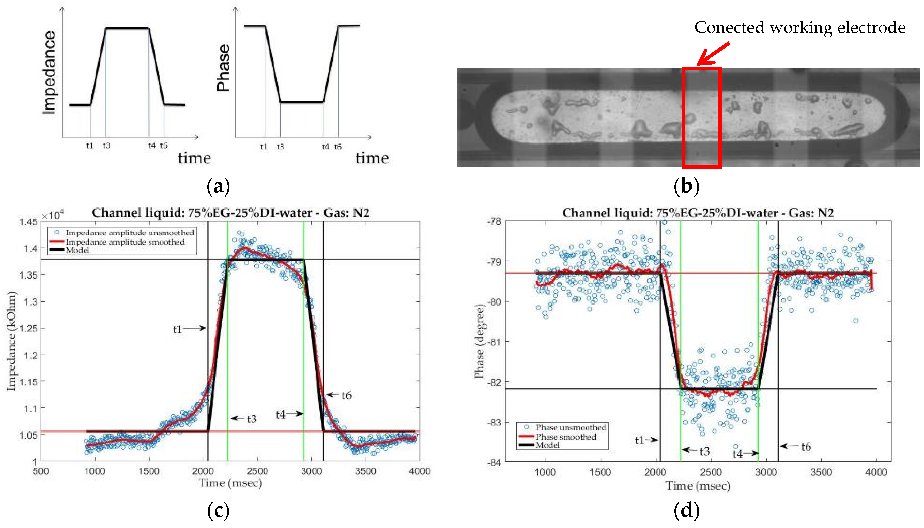
A housing for the reactor chip was made of PEEK; electrical connections were established using spring probes contacting the ITO contact pads, which connected to a HIOKI IM3536 LCR-meter. Continuous impedance measurements (20 kHz applied signal) were performed. The liquid (25% DI water-75% ethylene glycol) flow was provided via a syringe pump and gas for bubble generation was provided from house nitrogen, regulated through a gas flow meter (0.5 to 2 bar). Video of the two-phase slug flow with 1000 fps was recorded (MotionBLITZ EoSens mini2). A captured picture of a bubble with 2.3 mm length passing under a connected electrode is shown in Figure 4b.
In this step of the development, recorded frames with highspeed camera were used in order to correlate the electrical measurements. In Figure 4a, a model of the form of the electrical signal is presented. The relevant time points, however, are extracted from the video frames: t1 indicates the entry of the bubble cap under the working electrode, t3 the beginning of the bubble body, t4 entry of the trailing cap and t6 exit of the trailing cap. It is thus defined that the time point t1 (video timeframe, bubble cap entry to measurement region) is coincident with the start of the rise in the impedance values. Due to delay in the communication between the camera and the computer, there is a delay in the respective timelines.
The shown pulse model in Figure 4a was swept over the measured impedance signal, similar to a cross correlation. The variances of the data in three plateau regions (start–t1, t3–t4, t6–end) for each variation of the sweep were calculated and summed. The minimum value of the variance array (average of impedance amplitude and phase angle signal) was considered the best fit. Using the assumed model and fitting algorithm, the integrated electrica l sensor ove r the microchannel is suitable for two-phase flow detection and modeling.
4. Conclusions
This paper presents a glass/SU8 based microreactor with parallel plate ITO sensors on channel for studying bubble transport in a microchannel. The substrates are suitable for harsh photochemical reactions planned for future work. Using post-processing algorithms, the chip is able to analyze bubble geometry while allowing exposure for the photochemistry with transparent ITO electrodes.
Author Contributions
The study conception of the microchip was proposed by Cobry. Design, development and microchip fabrication, data acquisition, analysis and interpretation of data were performed by Talebi. Drafting of the manuscript was performed by Talebi and Cobry. Sengupta has been active as a research assistant in this project and helped in microfabrication process. This research was supported in the Laboratory for Design of Microsystems under the supervision of Woias.
Acknowledgments
Financial support by the German Research Foundation (DFG) through the Research Unit FOR 2383 ProMiSe under Grant No. Di 696/13-1 is gratefully acknowledged. We would also like to acknowledge Franz Richardt, and the staff at the IMTEK cleanroom as well as Dirk Ziegenbalg (University of Stuttgart) for helpful discussions on two-phase photochemical reactions for future work.
Conflicts of Interest
The authors declare no conflict of interest.
References
- Isgor, P.K.; Marcali, M.; Keser, M.; Elbuken, C. Microfluidic droplet content detection using integrated capacitive sensors. Sens. Actuators B Chem. 2015, 210, 669–675. [Google Scholar] [CrossRef]
- Vulto, P.; Huesgen, T.; Albrecht, B.; Urban, G.A. A full-wafer fabrication process for glass microfluidic chips with integrated electroplated electrodes by direct bonding of dry film resist. J. Micromech. Microeng. 2009, 19, 77001. [Google Scholar] [CrossRef]
- Iliescu, C.; Poenar, D.P.; Carp, M.; Loe, F.C. A microfluidic device for impedance spectroscopy analysis of biological samples. Sens. Actuators B Chem. 2007, 123, 168–176. [Google Scholar] [CrossRef]
- Gijsenbergh, P.; Puers, R. Permittivity-based void fraction sensing for microfluidics. Sens. Actuators A Phys. 2013, 195, 64–70. [Google Scholar] [CrossRef]
- Sabuncu, A.C.; Zhuang, J.; Kolb, J.F.; Beskok, A. Microfluidic impedance spectroscopy as a tool for quantitative biology and biotechnology. Biomicrofluidics 2012, 6, 34103. [Google Scholar] [CrossRef] [PubMed]
- Elbuken, C.; Glawdel, T.; Chan, D.; Ren, C.L. Detection of microdroplet size and speed using capacitive sensors. Sens. Actuators A Phys. 2011, 171, 55–62. [Google Scholar] [CrossRef]
Figure 1.
Figure 1. Microreactor design. (a) Exploded view; (b) Cross sectional schematic (not to scale); (c) Microchannel geometry; (d) Plan view of the assembled microreactor chip with integrated electrodes.
Figure 1.
Figure 1. Microreactor design. (a) Exploded view; (b) Cross sectional schematic (not to scale); (c) Microchannel geometry; (d) Plan view of the assembled microreactor chip with integrated electrodes.
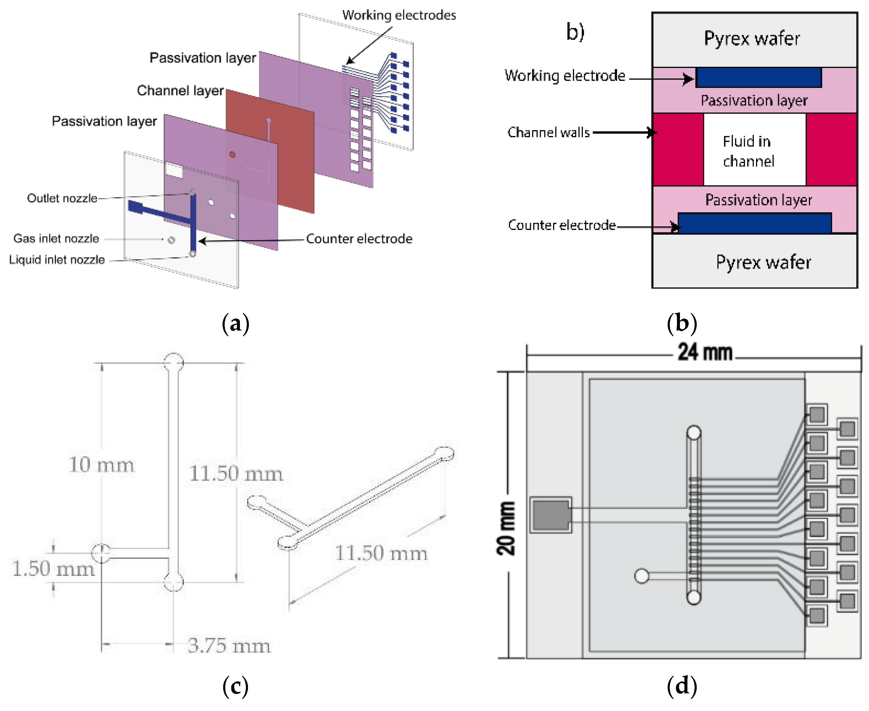
Figure 2.
Fabrication process flow. (a) Working electrode chip; (b) Ground electrode chip.

Figure 3.
(a) On-channel dry etched ITO electrodes; (b) Dry etched ITO electrode connection traces; (c) Dry etched ITO electrode contact pads.
Figure 3.
(a) On-channel dry etched ITO electrodes; (b) Dry etched ITO electrode connection traces; (c) Dry etched ITO electrode contact pads.

Figure 4.
Analysis of a bubble passing under the electrode. (a) Bubble signal model; (b) Bubble photo captured by highspeed camera; (c) Impedance signal fitted to model; (d) Phase signal fitted to model.
Figure 4.
Analysis of a bubble passing under the electrode. (a) Bubble signal model; (b) Bubble photo captured by highspeed camera; (c) Impedance signal fitted to model; (d) Phase signal fitted to model.
Publisher’s Note: MDPI stays neutral with regard to jurisdictional claims in published maps and institutional affiliations. |
© 2017 by the authors. Licensee MDPI, Basel, Switzerland. This article is an open access article distributed under the terms and conditions of the Creative Commons Attribution (CC BY) license (https://creativecommons.org/licenses/by/4.0/).
Share and Cite
MDPI and ACS Style
Talebi, M.; Cobry, K.; Sengupta, A.; Woias, P. Transparent Glass/SU8-Based Microfluidic Device with on-Channel Electrical Sensors. Proceedings 2017, 1, 336. https://doi.org/10.3390/proceedings1040336
AMA Style
Talebi M, Cobry K, Sengupta A, Woias P. Transparent Glass/SU8-Based Microfluidic Device with on-Channel Electrical Sensors. Proceedings. 2017; 1(4):336. https://doi.org/10.3390/proceedings1040336
Chicago/Turabian StyleTalebi, Mohammadmahdi, Keith Cobry, Ananya Sengupta, and Peter Woias. 2017. "Transparent Glass/SU8-Based Microfluidic Device with on-Channel Electrical Sensors" Proceedings 1, no. 4: 336. https://doi.org/10.3390/proceedings1040336