A Combined Temperature and Stress Sensor in 0.18 μm CMOS Technology †


1
Melexis Technologies SA, Chemin de Buchaux 38, 2022 Bevaix, Switzerland
2
Department of Microsystems Engineering (IMTEK), University of Freiburg, Germany
*
Author to whom correspondence should be addressed.
†
Presented at the Eurosensors 2017 Conference, Paris, France, 3–6 September 2017.
Proceedings 2017, 1(4), 340; https://doi.org/10.3390/proceedings1040340
Published: 8 August 2017
(This article belongs to the Proceedings of Proceedings of Eurosensors 2017, Paris, France, 3–6 September 2017)
Abstract
:This paper presents a solution for on-chip temperature and mechanical stress measurement in CMOS integrated circuits. Thereby both temperature and stress sensors are realized as resistive Wheatstone bridges. By design, both sensors show outputs affected by non-linearities and parasitic cross-sensitivities. The novelty presented in this work is to combine both non-ideal sensor outputs by applying a two-dimensional Newton-Raphson method to extract the actual values of temperature and mechanical stress which were obtained with errors of less than 0.5 K and 0.5 MPa.
1. Introduction
The accurate on-chip measurement of temperature free from the parasitic impact of package mechanical stress is of utmost importance for integrated sensors in order to provide a temperature-compensated output signal. Moreover, in Hall sensor microsystems the information of both temperature and mechanical stress is required for the compensation of thermal and stress-related cross-sensitivities [1]. However, CMOS temperature sensors are known to suffer from mechanical stress, often referred to as package shift [2]. Similarly, mechanical stress sensors are known to show a parasitic temperature dependence [3].
In contrast to previous attempts [2,4], this work does not try to minimize parasitic effects via optimization of the sensor designs. Quite to the contrary, the purpose of this work is to extract the accurate values of temperature and mechanical stress from the combination of both erroneous sensor outputs, removing non-linearities as well as cross-sensitivities. Therefore our solution is useful not only for the measurement of temperature and mechanical stress but may be applicable in general to a variety of multisensor systems.
2. Materials and Methods
2.1. Sensor Design and Implementation
The stress and temperature sensors consist of different CMOS in-plane resistors connected to Wheatstone bridges, as illustrated in the schematic diagrams of Figure 1a,d, respectively. The piezoresistive stress sensor combines highly doped n-type (Rn) and p-type (Rp) resistors, whereas for the temperature sensor p-well (Rpw) and p-type polysilicon (Rpp) resistors are used. For the sake of isotropy wrt. in-plane normal stresses, the two sensors are made of L-shaped resistors (RL), as detailed in [3,5]. The layouts of the sensors are shown in Figure 1b,c. They have sizes of 102 μm and 61 μm, respectively.
2.2. Sensor Response
The sensors provide a differential, ratiometric output voltage. Due to the combination of different resistor materials in the same bridge, an offset voltage appears, i.e., the output voltage at the reference stress 0 MPa and reference temperature 25 °C. This parasitic output signal is subtracted. The resulting offset-free signals Vσ and VT as a function of in-plane stress Δσip and temperature ΔT are described by [3,5]
where εσ, γσ, δσ, εT, γT, and δT denote the stress-related sensitivity and the first and second order temperature coefficients of the stress and temperature sensors, respectively. Vbias, Δσip, and ΔT denote the supply voltage and the deviations of in-plane mechanical stress and temperature, respectively, from the reference values. The coefficients εi, γi, and δi of (1) and (2) are obtained by calibration.
Vσ/Vbias = εσΔσip + γσΔT + δσΔT2,
VT/Vbias = εTΔσip + γTΔT + δTΔT2,
2.3. Extraction of Temperature and Mechanical Stress
Both sensor outputs depend on temperature and mechanical stress. Additionally, the thermal response is expected to show a quadratic term. Nevertheless, the accurate temperature and mechanical stress magnitude can be retrieved from the two erroneous sensor signals (1) and (2). In our case an iterative approach via a two-dimensional Newton-Raphson (2DNR) method was used, i.e.,
where xn+1 = [Δσip,n+1, ΔTn+1], xn= [Δσip,n, ΔTn] denote two successive iterations of the extracted stress and temperature vector, J, F = [Vσ,calc, VT,calc], and y = [Vσ,meas, VT,meas] denote the Jacobian matrix of partial derivatives of (1) and (2), the vector of calculated stress and temperature function values obtained from (1) and (2), and the vector of measured sensor outputs. The elements of J are derived straightforwardly from the polynomial expressions (1) and (2), i.e., ∂Vσ/∂Δσip = Vbiasεσ and ∂Vσ/∂ΔT = Vbias(γσ + 2δσΔT) and similarly for (2). The iteration of (3) is repeated until the residual difference |xn+1 − xn| is below a given threshold, e.g., 0.1 K and 0.1 MPa.
xn+1 = xn − [J]−1[F(xn) − y],
2.4. Experimental Setup
Samples were fabricated in standard 0.18 μm CMOS technology. Strips were cut from the wafer along the <110> (S#1) and <100> (S#2) crystal directions, as shown in Figure 2a,b, respectively. The strips containing the sensors were assembled to substrate PCBs and thereafter mounted in the four-point bending bridge, see Figure 2c,d. Via bending, the applied force gives rise to in-plane mechanical stress on the strip surface, as illustrated in Figure 2e. Placing the entire setup into a climate chamber allows to independently vary the temperature between 10 °C and 60 °C and the mechanical stress from 0 MPa to 75 MPa.
3. Results
3.1. Stress Response
The stress-related responses of the stress and temperature sensors were measured at Vbias = 3.3 V. The results are shown in Figure 3. The corresponding sensitivities were extracted to be εσ = −4.70 × 10⁻² GPa−1 and εT = −1.75 × 10⁻² GPa−1, respectively, by averaging S#1 and S#2. The difference between the sensitivities of S#1 and S#2 was below 2%, indicating the sensors isotropic response wrt. in-plane stresses.
3.2. Thermal Response
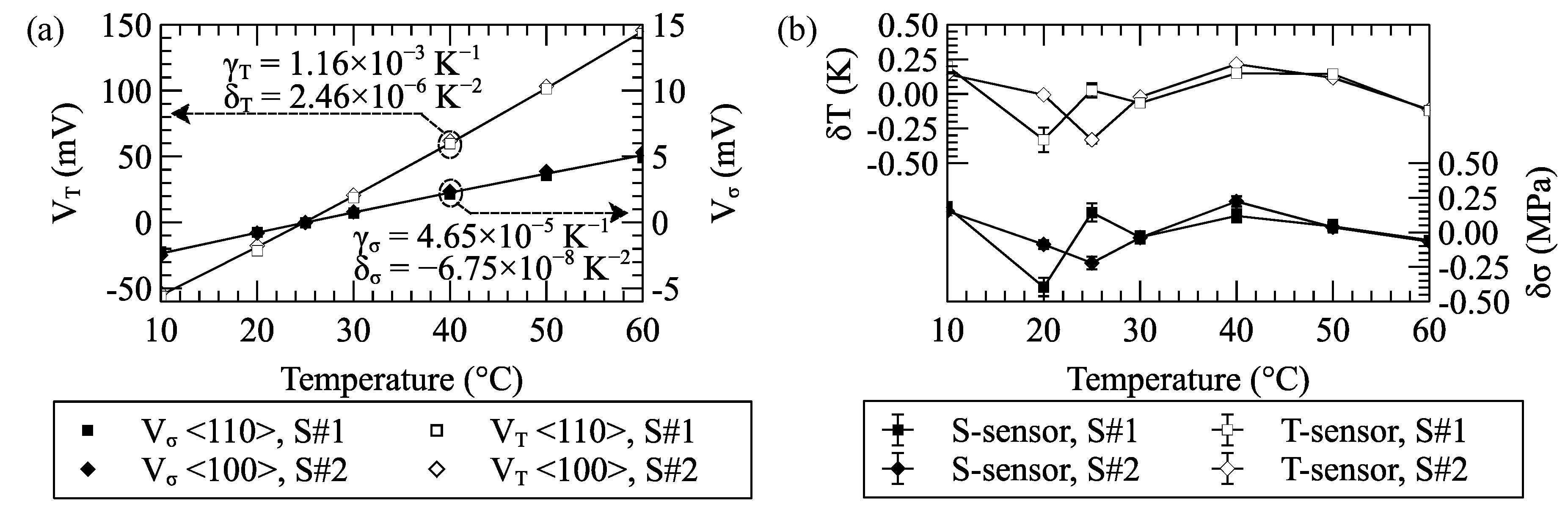
The thermal responses of Vσ and VT were measured and subsequently approximated by the second-order functions (1) and (2). The corresponding coefficients for the stress sensor were extracted as γσ = 4.65 × 10⁻⁵ K−1 and δσ = −6.75 × 10⁻⁸ K−2, by averaging S#1 and S#2, and γT = 1.16 × 10⁻³ K−1 and δT = 2.46 × 10⁻⁶ K−2, for the temperature sensor. The results are shown in Figure 4a. The differences of γσ and γT between S#1 and S#2 from the same wafer were observed to be below 10% and 1%, respectively.
3.3. Extraction of Temperature and Mechanical Stress, Residual Error
The 2DNR method (3) was applied to pairs of measured sensor output voltages. The obtained values of temperature and mechanical stress were found to match the externally applied test conditions, with differences below 0.5 K and 0.5 MPa, respectively, as shown in Figure 4b.
4. Discussion
A method to extract the values of temperature and mechanical stress in CMOS ICs was demonstrated using simple resistive bridge sensors. Thereby the proposed method successfully removes parasitic cross-sensitivities and non-linearities. In contrast to [2,4] no effort for transducer optimization, i.e., linearization and elimination of parasitic effects was necessary, as this regularization is achieved numerically.
Conflicts of Interest
The authors declare no conflict of interest. The founding sponsors had no role in the design of the study; in the collection, analyses, or interpretation of data; in the writing of the manuscript, and in the decision to publish the results.
References
- Huber, S.; Leten, W.; Ackermann, M.; Schott, C.; Paul, O. A Fully Integrated Analog Compensation for the Piezo-Hall Effect in a CMOS Single-Chip Hall Sensor Microsystem. IEEE Sens. J. 2015, 15, 2924–2933. [Google Scholar] [CrossRef]
- Souri, K.; Chae, Y.; Makinwa, K.A.A. A CMOS Temperature Sensor with a Voltage-Calibrated Inaccuracy of ±0.15 °C (3σ) from −55 °C to 125 °C. IEEE J. Solid State Circuits 2013, 48, 292–301. [Google Scholar] [CrossRef]
- Huber, S.; Schott, C.; Paul, O. Package Stress Monitor to Compensate for the Piezo-Hall Effect in CMOS Hall Sensors. IEEE Sens. J. 2013, 13, 2890–2898. [Google Scholar] [CrossRef]
- Haas, S.; Schramm, M.; Reuter, D.; Loebel, K.-U.; Horstmann, J.T.; Gessner, T. Direct integrated strain sensors for robust temperature behavior. In Proceedings of the TRANSDUCERS Conference, Anchorage, AK, USA, 21–25 June 2015; pp. 184–187. [Google Scholar]
- Huber, S.; Laville, A.; Schott, C.; Paul, O. A bridge-type resistive temperature sensor in CMOS technology with low stress sensitivity. In Proceedings of the IEEE Sensors Conference, Valencia, Spain, 2–5 November 2014; pp. 1455–1458. [Google Scholar]
Figure 1.
Stress and temperature sensor schematic diagrams (a,d) and layouts (b,c) in standard 0.18 μm CMOS technology. The stress sensor is realized with highly doped n-type (Rn) and p-type (Rp) resistor segments, whereas p-well (Rpw) and p-poly (Rpp) resistor segments are used for the temperature sensor. The individual resistor segments are connected to L-shaped, orthogonal pairs (RL) for their stress response to be isotropic with respect to in-plane stresses.

Figure 2.
Experimental setup including a diagram of the samples strips orientations along the (a) <110> and (b) <100> crystal directions, (c) micrograph of a strip assembly, (d) photograph and (e) schematic diagram of the four-point bending bridge operated in a climate chamber.
Figure 2.
Experimental setup including a diagram of the samples strips orientations along the (a) <110> and (b) <100> crystal directions, (c) micrograph of a strip assembly, (d) photograph and (e) schematic diagram of the four-point bending bridge operated in a climate chamber.

Figure 3.
Stress responses of the stress and temperature sensors at T = 25 °C and Vbias = 3.3 V on Si strips oriented along the <110> (S#1) and <100> (S#2) crystal directions. Linear functions were fitted to the measurements, i.e., Vσ/Vbias = εσΔσip, and similarly for VT.
Figure 3.
Stress responses of the stress and temperature sensors at T = 25 °C and Vbias = 3.3 V on Si strips oriented along the <110> (S#1) and <100> (S#2) crystal directions. Linear functions were fitted to the measurements, i.e., Vσ/Vbias = εσΔσip, and similarly for VT.
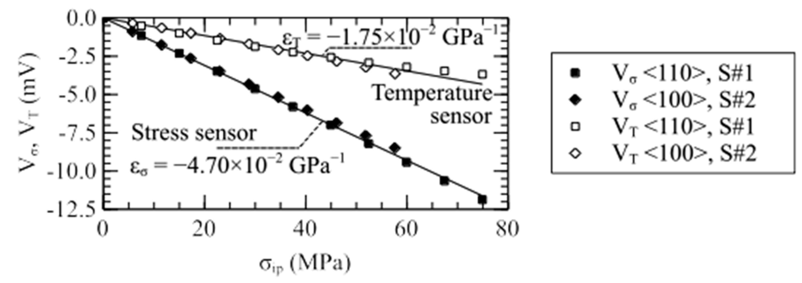
Figure 4.
(a) Thermal responses of the temperature and stress sensors at zero stress and Vbias = 3.3 V. Second-order functions (1), (2) were fitted to the measurements to account for the non-linear thermal behavior of the underlying resistive materials. (b) Residual errors of the extracted temperature and stress values. Error bars indicate the standard deviation for all applied stresses at the particular temperature. Solid lines are guides to the eye.
© 2017 by the authors. Licensee MDPI, Basel, Switzerland. This article is an open access article distributed under the terms and conditions of the Creative Commons Attribution (CC BY) license (https://creativecommons.org/licenses/by/4.0/).
Share and Cite
MDPI and ACS Style
Huber, S.; François, S.; Paul, O. A Combined Temperature and Stress Sensor in 0.18 μm CMOS Technology. Proceedings 2017, 1, 340. https://doi.org/10.3390/proceedings1040340
AMA Style
Huber S, François S, Paul O. A Combined Temperature and Stress Sensor in 0.18 μm CMOS Technology. Proceedings. 2017; 1(4):340. https://doi.org/10.3390/proceedings1040340
Chicago/Turabian StyleHuber, Samuel, Samuel François, and Oliver Paul. 2017. "A Combined Temperature and Stress Sensor in 0.18 μm CMOS Technology" Proceedings 1, no. 4: 340. https://doi.org/10.3390/proceedings1040340