Proceeding Paper

Development of All-Around SiO2/Al2O3 Gate, Suspended Silicon Nanowire Chemical Field Effect Transistors Si-nw-ChemFET †

Laboratory for Analysis and Architecture of Systems (LAAS-CNRS), Université de Toulouse, F-31400 Toulouse, France
*
Author to whom correspondence should be addressed.
Presented at the Eurosensors 2017 Conference, Paris, France, 3–6 September 2017.
Proceedings 2017, 1(4), 419; https://doi.org/10.3390/proceedings1040419
Published: 8 August 2017
(This article belongs to the Proceedings of Proceedings of Eurosensors 2017, Paris, France, 3–6 September 2017)

Abstract

:
We present a sensor platform associated to silicon-nanowire chemical field effect transistors (Si-nw-ChemFET). Innovations concern the use of networks of suspended silicon N+/P/N+ nanowires as conducting channel, the realization by thermal oxidation and Atomic-Layer Deposition (ALD) of a SiO2/Al2O3 gate insulator all-around the silicon nanowires, and their final integration into covered SU8-based microfluidic channels. The Si-nw-MOSFET/ChemFET fabrication process and electrical/electrochemical characterizations are presented. The fabrication process did not need an expensive and time-consuming e-beam lithography, but only fast and “low cost” standard photolithography protocols. Such microdevice will provide new opportunities for bio-chemical analysis at the micro/nanoscale.

1. Introduction

Chemically sensitive Field Effect Transistors (ChemFET) are microsensors derived by Metal Oxide Semiconductor Field Effect Transistors (MOSFET) [1]. These are electronic microsensors designed to measure the pH. ChemFETs have shown interesting properties for the detection in liquid phase and have been functionalized for many applications [1,2]. Nevertheless, to open the door to new innovative applications for ChemFET-based microsensors, it is necessary to increase their sensitivity, to decrease response times and their detection limit. To meet this challenge, the development of nanotransistor based on silicon nanowire Si-nw-ChemFET was proposed [3,4]. In this field, surrounding gate seems the ideal candidate: indeed, low channel dimensions provide new detection mechanisms as well as analysis of micro/nano-volumes, allowing to work at the single cell level [4]. Thus, the development of suspended silicon nanowires should still improve Si-nw-ChemFET detection properties in liquid phase, providing the integration of well-controlled chemically sensitive gate insulators all-around the Si-nw-based conductive channel.

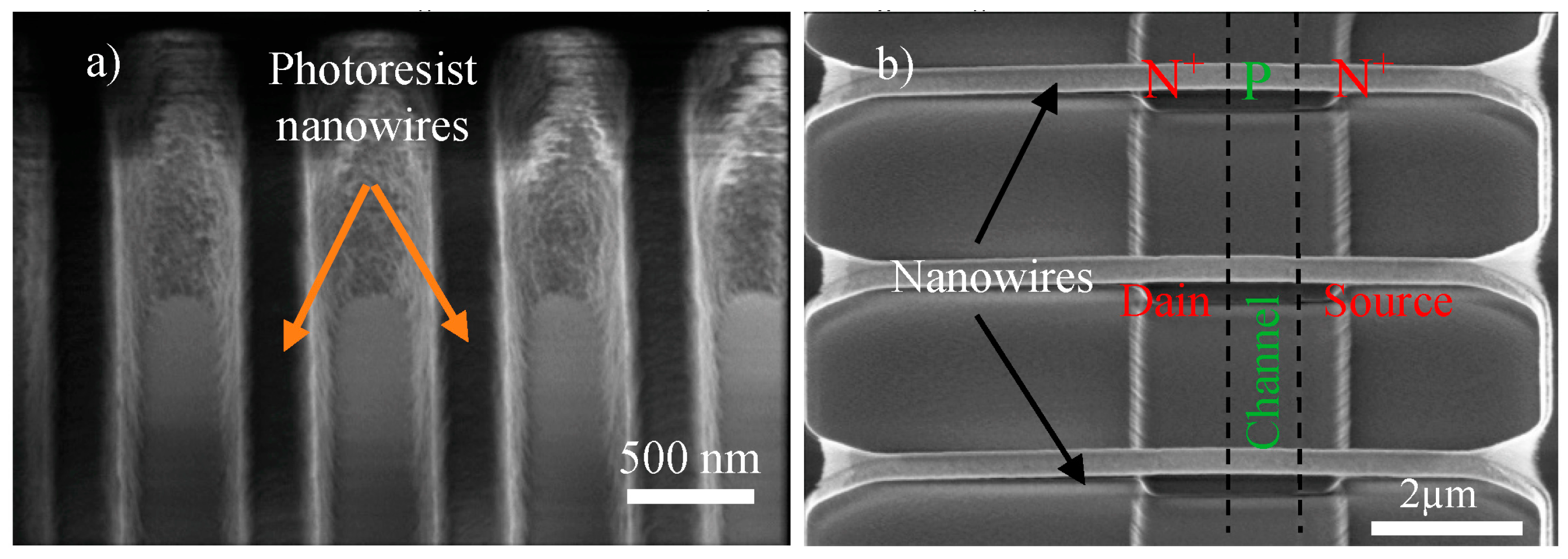
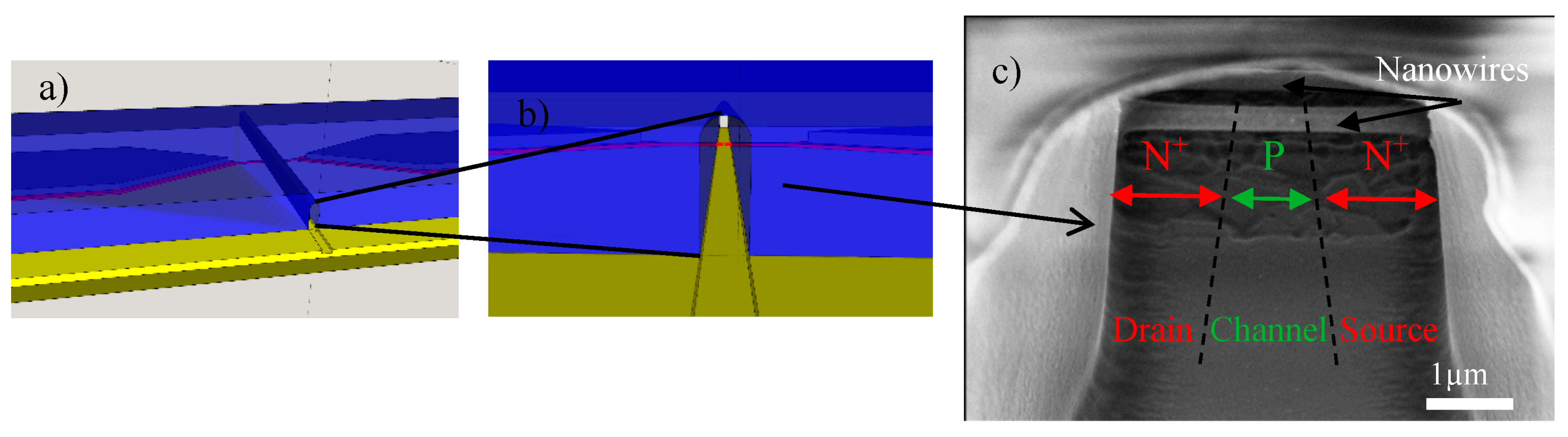
2. Device Fabrication

6-inch SOI wafers (Silicon On Insulator, P type, 1015 atoms/cm3) were used. These devices consist in single and networked silicon nanowires field effect transistors. Different wire lengths, gate lengths and number of parallel wires were fabricated. First, source and drain areas were N doped (1020 atoms/cm3) with arsenic ion implantation. Two different gate length were realized, 0.9 µm and 3.9 µm. To fabricate silicon nanowires, projection photolithography with a Canon FPA-3000i4 stepper and an AZ ECI 3012 photoresist were employed. After optimizations, were achieved on a single chip, patterns of transistors with a single nanowire as channel, next to patterns of transistors with 100 nanowires parallel network (Figure 1a). The goal is to compare in the future, the pros and cons of each structure, in terms of limit of detection and/or sensitivity for biochemical applications. Once photoresist nanowires were optimized, nanopatterns were transferred in silicon thanks to a reactive ion etching. After optimization, 200 nm × 170 nm rectangle section nanowires were obtained with a perfect reproducibility. Two different densities of network were realized: 20 and 100 nanowires over a width of 80 µm. Thus, using SOI wafers, networks of suspended silicon nanowires were successfully integrated (Figure 1b). Then, the realization of the gate structure was performed. After RCA cleaning, a dry thermal oxidation of 22 nm was achieved and an alumina film of 26 nm was deposited by ALD. The advantage of this technique is to deposit extremely conformal films all around the nanowires, while providing well-controlled thicknesses [5]. Thus, a SiO2/Al2O3 gate was integrated all-around the silicon nanowire. This Al2O3 layer was used as a gate chemically sensitive layer as well as the microdevice passivation layer in liquid phase [3,6].
Once the gate/source/drain metallic contacts and interconnections were ended, Si-nw-MOSFET and Si-nw-ChemFET were fabricated. Then, using a specific SU8-3D technique [7], covered 5 µm width microfluidic channels were finally realized in order to deal with liquid phase analysis at the microscale (Figure 2).

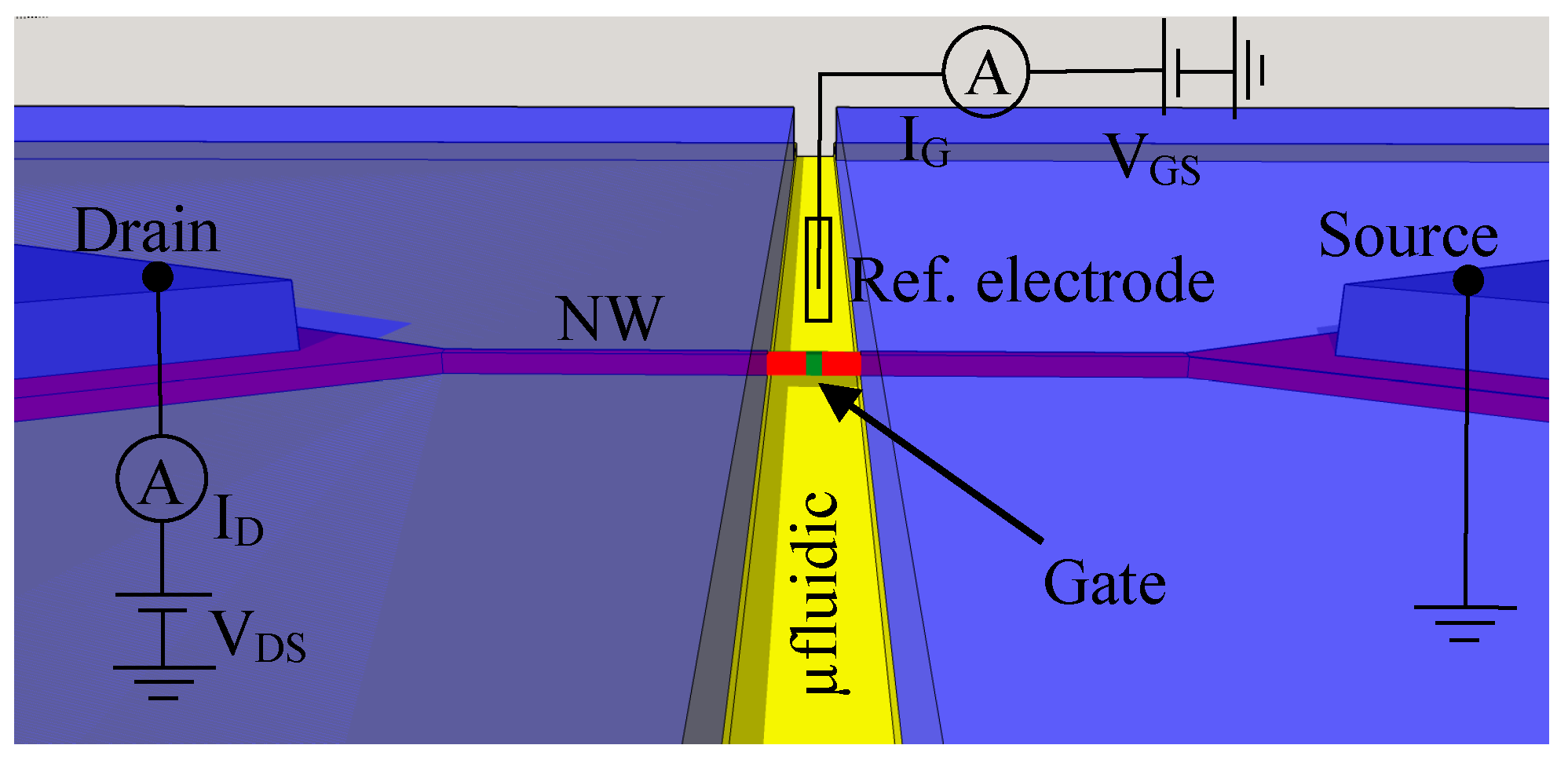
3. Device Characterizations

Si-nw-MOSFET/ChemFET were characterized electrically and electrochemically using standard I-V experiments (Figure 3). The MOSFET works without liquid, so it makes easier some characterizations. It allows to check the quality of the manufacturing process, and to discriminate problems due to the transistor from those related to the microfluidics.

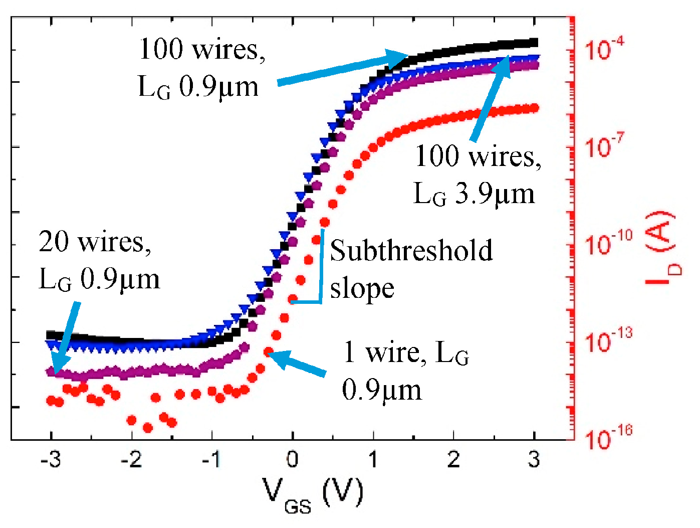
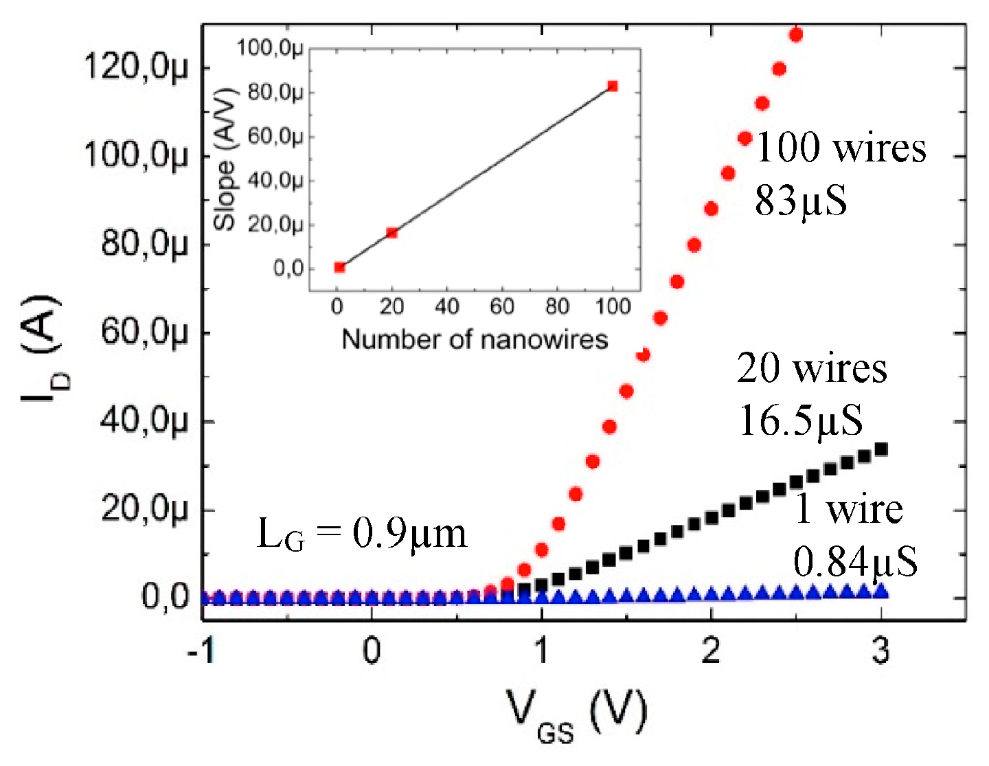
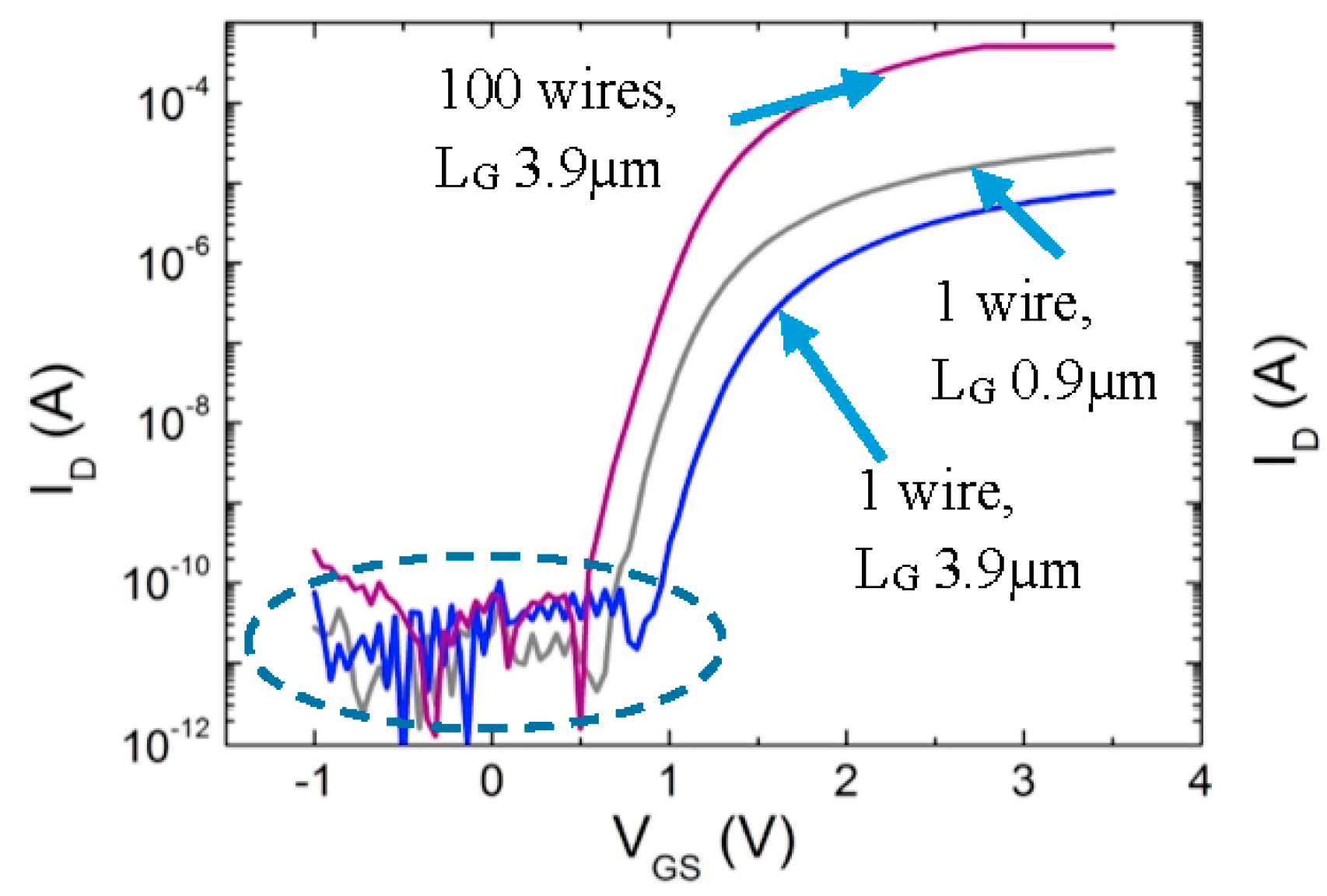
3.1. Si-nw-MOSFET Characterizations

The threshold voltage of 42 transistors was measured and the mean value was 0.62 V with a standard deviation of only 0.26 V. That shows the quality of the SiO2/ALD-Al2O3 gate dielectric and the Si/SiO2 interface. The influence of 2 parameters on electric characteristics was studied: the number of parallel nanowires (1, 20 and 100) and the gate length LG (0.9 µm “short” and 3.9 µm “long”), the length of the nanowires is 10 µm. Firstly, very low subthreshold (IOFF) currents (7.10−14 A for VGS = −2 V, VDS = 0.1 V) were obtained for a parallel network of 100 nanowires (Figure 4). This leakage current is the same for both gate lengths and proportional to the number of parallel nanowires. Therefore, it allows to estimate the leakage current of X nanowires. The leakage current through the gate dielectric (IG) is lower than 10−15 A (limit of the measuring instrument) for 100 parallel nanowires under 3 V. So, the IG current is lower than 10−17 A for one nanowire and shows the insulation quality of the SiO2/Al2O3 double layer. The number of parallel nanowires and the gate length does not influence the subthreshold slope, which is 6 decades/V. The ratio ION/IOFF is about 109, thanks to the very low IOFF current. The transconductance is 4.3 times higher for nanowires with the short gate length in comparison with the long gate length, exactly the length ratio between the long and short gate lengths. The transconductance is also proportional to the number of parallel nanowires (Figure 5). All these characterizations have confirmed the good operation of Si-nw-MOSFET.

3.2. Si-nw-ChemFET Characterizations

The Si-nw-ChemFET is like a Si-nw-MOSFET which gate metallization is replaced by a microfluidic channel. Si-nw-ChemFETs were characterized in liquid phase with a specific setup. The liquid was polarized with an Ag/AgCl/KClsat reference electrode. Like for the study of Si-nw-MOSFET, the influence of 2 parameters on electric characteristics was studied: the number of parallel nanowires (1 and 100) and the gate length LG (0.9 µm and 3.9 µm), the length of the nanowires is 10 µm. The subthreshold leakage current (IOFF) and the leakage current through the gate dielectric (IG), for 100 parallel nanowires, were not measurable because they were lower than the limit of the characterization setup (5.10−11 A) (Figure 6). That means an IOFF current and an IG current lower than 5.10−13A for one nanowire. These very low leakage currents allow a high ION/IOFF ratio reaching at least 107 for one nanowire and 108 for 100 parallel nanowires. Concerning the subthreshold slope, excellent characteristics were obtained, with 8 decades/V. Like for the Si-nw-MOSFET, this value is independent of the number of parallel nanowires and gate length. As for the Si-nw-ChemFET, the transconductance is inversely proportional to the gate length. The Nernstian response to pH variations of 58 mV/pH is in agreement with theory (Figure 7). All these characterizations have shown the good behavior of Si-nw-ChemFET in liquid phase, and demonstrated the performances of the bilayer SiO2/ALD-Al2O3 for ChemFET fabrication.

4. Discussion

These good results are due to the excellent control of the nw-Si/insulator/electrolyte interface using an all-around gate with high dielectric capacity. Junctions on the nanowires make possible to increase the ION/IOFF ratio by decreasing strongly the current when the transistors are in their blocked mode. The reduction of the gate length make possible to increase the transconductance, it is interesting for the amplification of biochemical signals like action potentials [8]. The bilayer SiO2/Al2O3 is advantageous because the Si/SiO2 allows a very good interface, which is highly important for a MOSFET based component. The second layer, the ALD-Al2O3 is a good (high-k) insulator in liquid phase. That is why gate leakage currents are so low. Thanks to Al2O3, Si-nw-ChemFET shows near Nernstian responses to pH changes. This allows to hope for a much better signal-to-noise ratio for biological applications than planar ChemFET.

5. Conclusions

Silicon nanowire based MOSFET and ChemFET (Si-nw-MOSFET and Si-nw-ChemFET) were designed, realized and presented in this paper. Electrical and electrochemical characterizations have shown good results. In short-term perspective, thanks to the small dimensions of the sensing area and to improved detection performances, the accurate and reproducible monitoring of biological metabolisms is expected on living cells using suspended Si-nw-ChemFET.

Acknowledgments

This work was partly supported by LAAS-CNRS micro and nanotechnologies platform, member of the French RENATECH network.

Conflicts of Interest

the authors declare no conflict of interest.

References

  1. Bergveld, P. Development of an ion-sensitive solid-state device for neurophysiological measurements. IEEE Trans. Biomed. Eng. 1970, BME-17, 70–71. [Google Scholar] [CrossRef] [PubMed]
  2. Fromherz, P. Joining microelectronics and microionics: Nerve cells and brain tissue on semiconductor chips. Solid-State Electron. 2008, 52, 1364–1373. [Google Scholar] [CrossRef]
  3. Knopfmacher, O.; Keller, D.; Calame, M.; Schönenberger, C. Dual Gated Silicon Nanowire Field Effect Transistors. Procedia Chem. 2009, 1, 678–681. [Google Scholar] [CrossRef]
  4. Duan, X.; Gao, R.; Xie, P.; Cohen-Karni, T.; Qing, Q.; Choe, H.S. Tian, B.; Jiang, X.; Lieber, C.M. Intracellular recordings of action potentials by an extracellular nanoscale field-effect transistor. Nat. Nanotechnol. 2012, 7, 174–179. [Google Scholar]
  5. Elam, J.; Routkevitch, D.; Mardilovich, P.P.; George, S.M. Conformal Coating on Ultrahigh-Aspect-Ratio Nanopores of Anodic Alumina by Atomic Layer Deposition. Chem. Mater. 2003, 18, 3507–3517. [Google Scholar] [CrossRef]
  6. Matsuo, T.; Esashi, M. Methods of isfet fabrication. Sens. Actuators 1981, 1, 77–96. [Google Scholar] [CrossRef]
  7. Larramendy, F.; Bendali, A.; Blatche; Blatché, M.C.; Mathieu, F.; Picaud, S.; Temple-Boyer, P.; Nicu, L. MISFET-based biosensing interface for neurons guided growth and neuronal electrical activities recording. Sens. Actuators B Chem. 2014, 203, 375–381. [Google Scholar] [CrossRef]
  8. Fromherz, P. Electrical Interfacing of Nerve Cells and Semiconductor Chips. Chemphyschem 2002, 3, 276–284. [Google Scholar] [CrossRef]
Figure 1. SEM views, (a) of a network of photoresist nanowires, before reactive ion etching; (b) of silicon nanowires after gate insulator completion (tilt 52°).
Proceedings 01 00419 g001
Figure 2. (a,b) schematic views of the Si-nw-ChemFET and the microfluidic channel; (c) SEM view of suspended silicon nanowires inside a covered microfluidic channel (tilt 52°).
Proceedings 01 00419 g002
Figure 3. Schematic view of the polarization for Si-nw-ChemFET characterizations.
Proceedings 01 00419 g003
Figure 4. Id(Vgs) characterizations of Si-nw-MOSFETs, semi-logarithmic scale. (Vds = 0.1 V).
Proceedings 01 00419 g004
Figure 5. Id(Vgs) characterizations of Si-nw-MOSFETs, linear scale. (Vds = 0.1 V).
Proceedings 01 00419 g005
Figure 6. Id(Vgs) characterizations in liquid phase of Si-nw-ChemFETs, with a semi-logarithmic scale. (Vds = 1 V).
Proceedings 01 00419 g006
Figure 7. Id(Vgs) characterizations in liquid phase of Si-nw-ChemFET, with a semi-logarithmic and a linear scale, for three different pH. (Vds = 1 V).
Proceedings 01 00419 g007

