An Electromagnetically-Driven Piezoresistively Sensed CMOS MEMS Scanning Mirror for Projection Display †

Department of Electrical Engineering, National Tsing Hua University, Hsinchu 30013, Taiwan
*
Author to whom correspondence should be addressed.
†
Presented at the Eurosensors 2017 Conference, Paris, France, 3–6 September 2017.
Proceedings 2017, 1(4), 353; https://doi.org/10.3390/proceedings1040353
Published: 8 August 2017
(This article belongs to the Proceedings of Proceedings of Eurosensors 2017, Paris, France, 3–6 September 2017)
Abstract
:Bi-axial MEMS scanning mirrors are considered the key component for applications like laser scanning projectors and Lidars. Most studies have shown fabricated devices driven by open-loop operation without sensing, making it difficult to meet the requirements for practical applications. To facilitate bi-axial closed-loop operation, this work presents an electro magnetically-driven scanning mirror with piezoresistive sensing conveniently implemented in a CMOS (complementary metal oxide semiconductor) process. The measured resonant frequencies with respect to the slow and fast axes are 4.3 and 36.05 kHz, respectively, with the aim to provide SXGA display resolution.
1. Introduction
A typical laser scanning projection engine consists of lasers to form light beams with a small numerical aperture and a 2D scanning mirror that deflects the beams to form images pixel by pixel. The produced images are always in focus at different distances without additional focusing optics. For successful image projection, it is crucial to maintain the synchronization between the calculated pixel position and the actual mirror motion, which requires sensitive detection of mirror’s position. A raster scanning mirror needs to be driven to resonance for scanning in the horizontal direction (fast axis) under closed-loop operation. The vertical scan (slow-axis) may also need to be closed-loop controlled to eliminate undesired oscillatory motion at under-damped condition. However, the idea is often hindered by the microfabrication capability to provide simultaneous driving and sensing. Therefore only few micro-scanners have demonstrated on-chip sensing capabilities [1,2,3]. As a first attempt to integrate CMOS in this work, the implementation conveniently provides piezoresistive sensing to the electromagnetically-driven scanning mirror. Initial measurement of bi-axial scanning is demonstrated.
2. Materials and Methods
The bi-axial scanning mirror is designed and fabricated by using a 0.35-μm 2P4M (two-polysilicon-four-metal) process. As shown by the top view schematic in Figure 1, the outer frame of the micro-scanner contains the coils carrying both the slow (x) and fast-axis (y) driving signals to produce the Lorentz force with the magnetic fields applied at a 45° angle. The desired anti-phase motion with respect to the fast axis is indirectly coupled through the motion of the frame [4]. Polysilicon piezoresistors are placed at the ends of supporting beams to detect the bi-axial motions. The CMOS MEMS technology not only provides the desired driving and sensing elements, but also the much needed convenient wiring and shielding between the signals which are not commonly available in many MEMS processes. The two resonant modes for the raster scanning mirror are simulated to be 0.97 kHz and 43.9 kHz, respectively, as shown in Figure 2. The latter is the anti-phase rocking mode where the frame moves in opposite direction with respect to the mirror. The simulated in-phase rocking mode is located at 8.1 kHz.
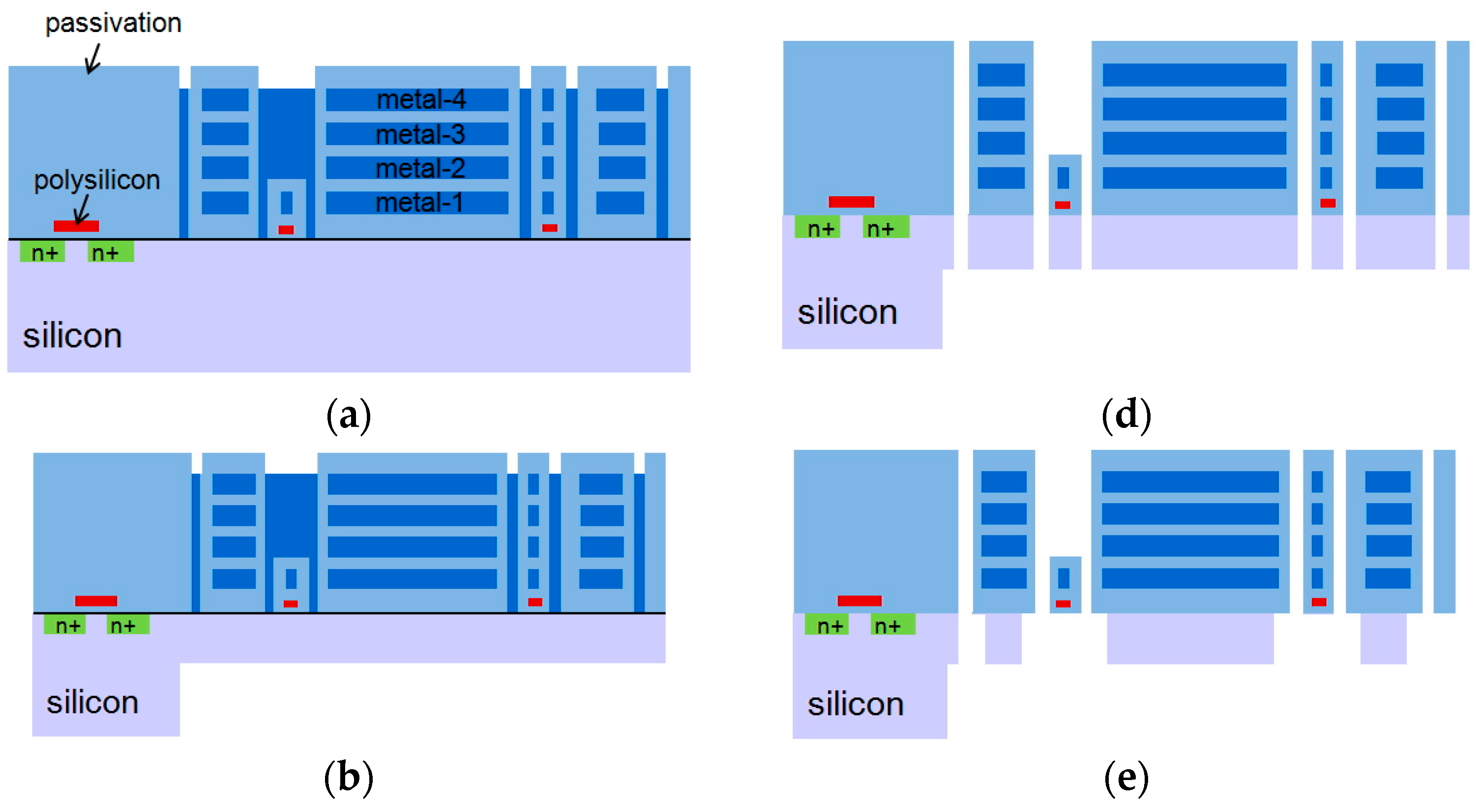
Post CMOS fabrication of the bi-axial scanning micro-mirror is described by the cross-sectional views in Figure 3. After the conventional CMOS process, backside deep reactive ion etch of silicon is firstly performed to define the structural thickness (~40 μm). Then the front-side stacked metal and via layers are removed by wet etch, followed deep reactive ion etch of silicon to form the structure. Isotropic XeF2 etch is performed next to remove the silicon underneath the springs along the slow axis. Finally, the top passivation is removed by dielectric reactive ion etch to expose the top metal of bond pads and that of the micro-mirror for laser beam reflection.
3. Results
Micrograph of the CMOS chip after post fabrication is shown in Figure 4a. The chip was wirebonded to a printed circuit board and placed at a 45° angle with respect to the two neodymium (NdFeB) magnets (2 cm × 4 cm each), which produced a magnetic field of 0.45 Tesla. Figure 4b shows the scanning electron micrograph of the released scanning mirror.
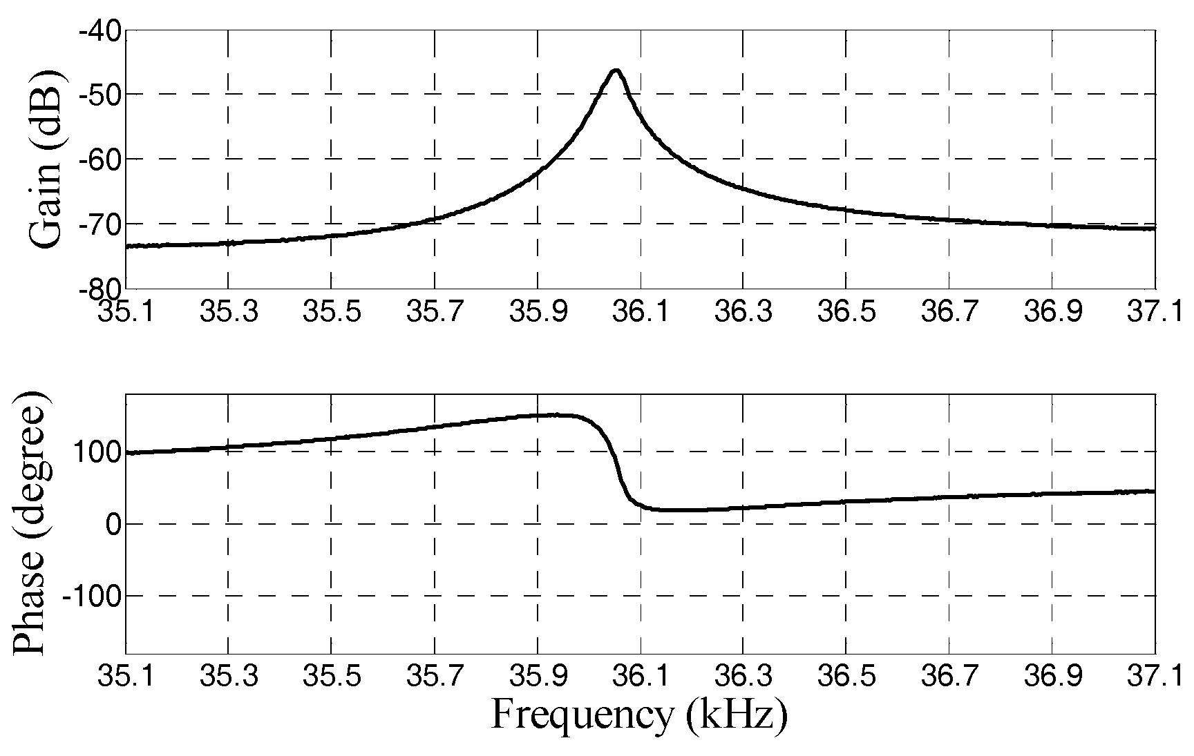
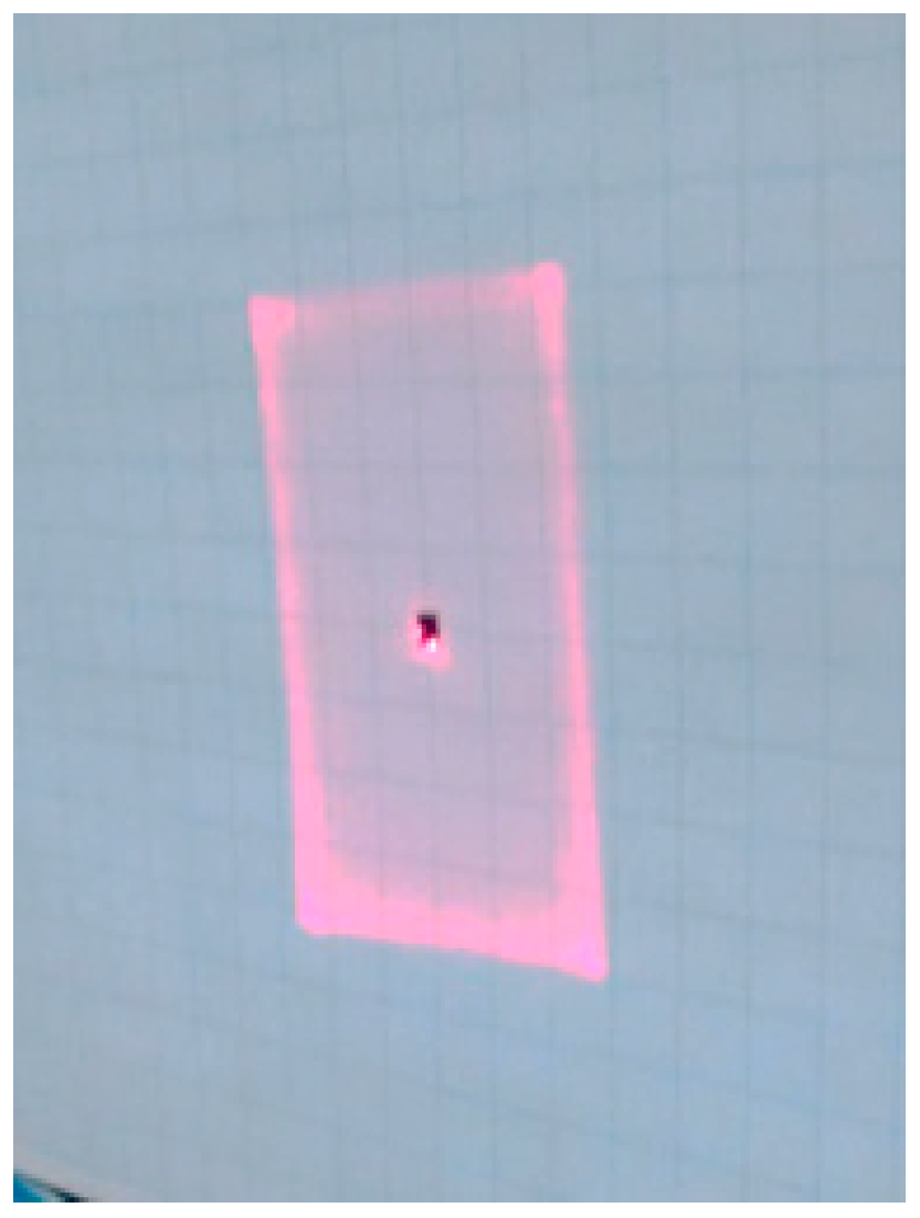
Frequency response of the scanning mirror was measured by laser Doppler vibrometer (LDV). Figure 5 shows that the measured slow-axis, in-phase and anti-phase rocking modes are at 4.3, 17.9 and 36.6 kHz, respectively. Deviations from the simulated values were attributed to the uneven silicon thickness after post fabrication. Oscillation of the anti-phase mode along the fast axis needs to be achieved by closed-loop operation that meets Barkhausen’s criteria. The frequency response of the electromagnetically-driven piezoresistively sensed scanning mirror was measured as shown in Figure 6 by a network analyzer (Agilent 4395A). Both the gain and phase at the fast-axis resonant frequency were compensated to achieve a loop gain and phase close to 0 dB and 0°, respectively. After compensation, the scanning mirror was successfully driven to oscillation as shown by the measured driving and sensed waveforms in Figure 7. Bi-axial laser projection was also successfully produced by the CMOS MEMS scanning mirror as shown in Figure 8. However, the produced optical angles were relatively small with respect to the applied current (~0.7 deg/mA for fast axis).
4. Conclusions
This work presents the first electromagnetically-driven scanning mirror with piezoresistive sensors for bi-axial laser scanning projection. Implementation of the driving and sensing elements is greatly facilitated by the CMOS MEMS fabrication. Closed-loop operation at the fast-axis resonant mode is successfully demonstrated. The current design is aimed at providing SXGA display resolution. The measured optical angles are relatively small, and need to be improved in the future.
Acknowledgments
This work is supported by the Ministry of Science and Technology, Taiwan. We are very grateful to the National Chip Implementation Center for support of chip fabrication and the National Center for High-Performance Computing for support of simulation software.
Conflicts of Interest
The authors declare no conflict of interest.
References
- Hofmann, U.; Janesm, J.; Quenzerm, H.-J. High-Q MEMS resonators for laser beam scanning displays. Micromachines 2012, 3, 509–528. [Google Scholar] [CrossRef]
- Hung, A.; Lai, H.; Lin, T.W.; Fu, S.G.; Lu, M.S.-C. Electrostatically-driven 2D micro-scanning mirror with capacitive sensing for projection display. Sens. Actuators A Phys. 2015, 222, 122–129. [Google Scholar] [CrossRef]
- Drabe, C.; Kallweit, D.; Dreyhaupt, A.; Grahmann, J.; Schenk, H.; Davis, W. Bi-resonant scanning mirror with piezoresistive position sensor for WVGA laser projection systems. In Proceedings of the 8252 SPIE, MOEMS and Miniaturized Systems XI, San Francisco, CA, USA; Bellingham, WA, USA, 24–25 January 2012; p. 825209. [Google Scholar]
- Yalcinkaya, A.D.; Urey, H.; Brown, D.; Montague, T.; Sprague, R. Two-axis electromagnetic microscanner for high resolution displays. J. Microelectromech. Syst. 2006, 15, 786–794. [Google Scholar] [CrossRef]
Figure 1.
Top view schematic of the bi-axial scanning mirror design.
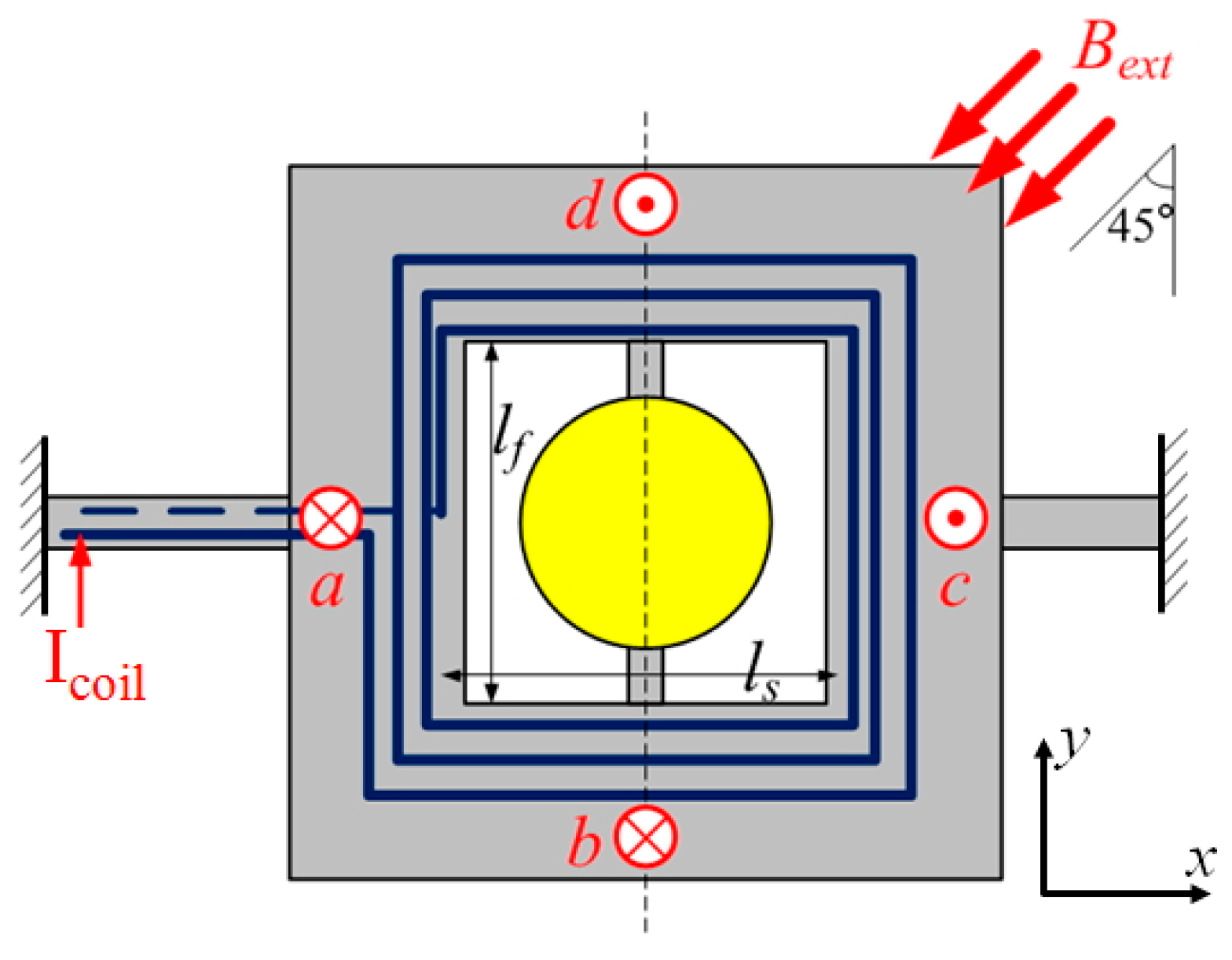
Figure 2.
Finite-element simulation of the slow- and fast-axis modes in (a) and (b).

Figure 3.
Post CMOS fabrication of the bi-axial scanning micro-mirror: (a) after CMOS process; (b) backside deep reactive ion etch of silicon to define the structural thickness; (c,d) wet etch of stacked metal and via layers followed by front-side deep reactive ion etch of silicon to form the structure; (e) XeF2 silicon etch; (f) dielectric reactive ion etch of the top passivation to expose the top metal of micro-mirror and bond pads.

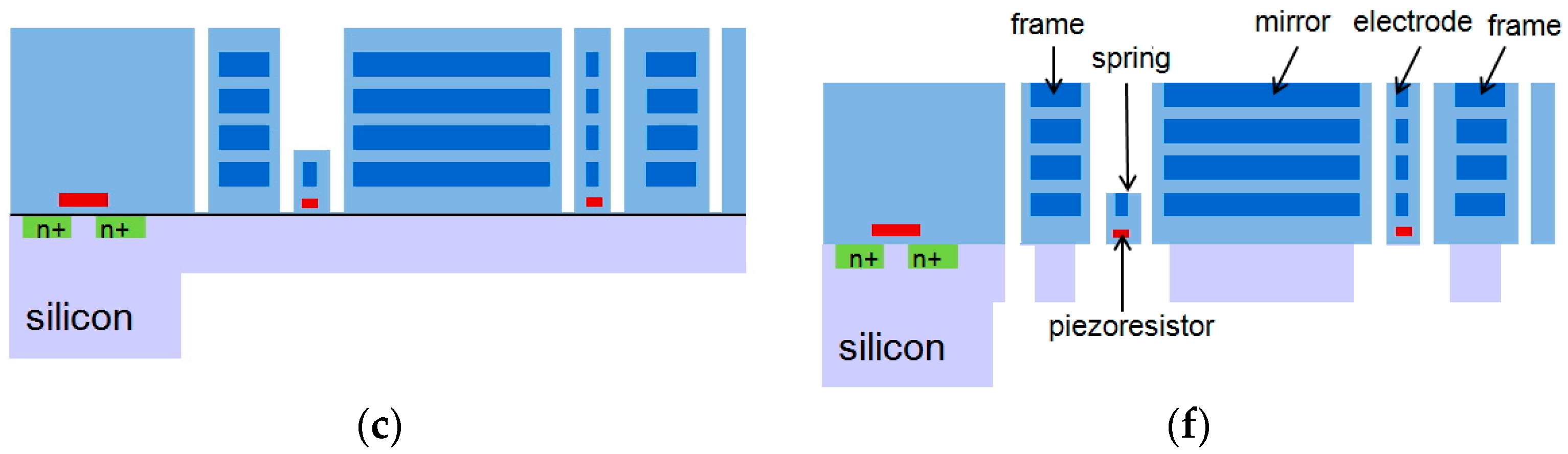
Figure 4.
(a) Micrograph of the CMOS chip. (b) Scanning electron micrograph of the released scanning mirror.
Figure 4.
(a) Micrograph of the CMOS chip. (b) Scanning electron micrograph of the released scanning mirror.
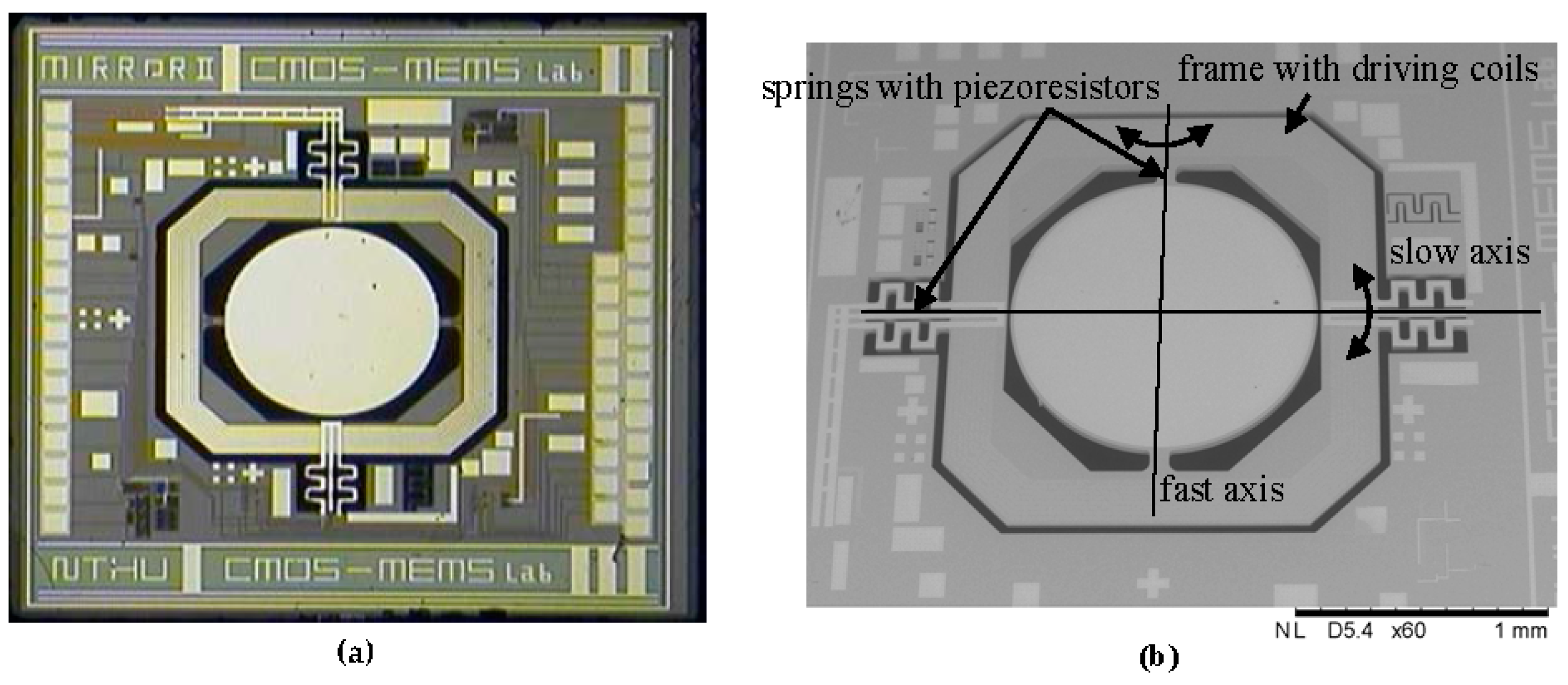
Figure 5.
Measured mechanical modes of the CMOS MEMS scanner. The measured slow-axis and anti-phase fast-axis modes are 4.3 and 36.05 kHz, respectively.
Figure 5.
Measured mechanical modes of the CMOS MEMS scanner. The measured slow-axis and anti-phase fast-axis modes are 4.3 and 36.05 kHz, respectively.
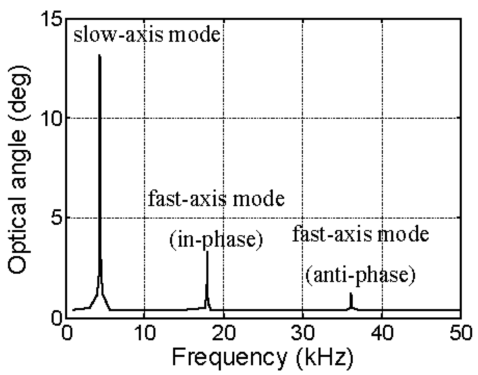
Figure 6.
Measured frequency response of the electromagnetically-driven piezoresistively sensed scanning mirror.
Figure 6.
Measured frequency response of the electromagnetically-driven piezoresistively sensed scanning mirror.

Figure 7.
Measured sensed and driving signals when the anti-phase mode is driven to oscillation by closed-loop operation.
Figure 7.
Measured sensed and driving signals when the anti-phase mode is driven to oscillation by closed-loop operation.
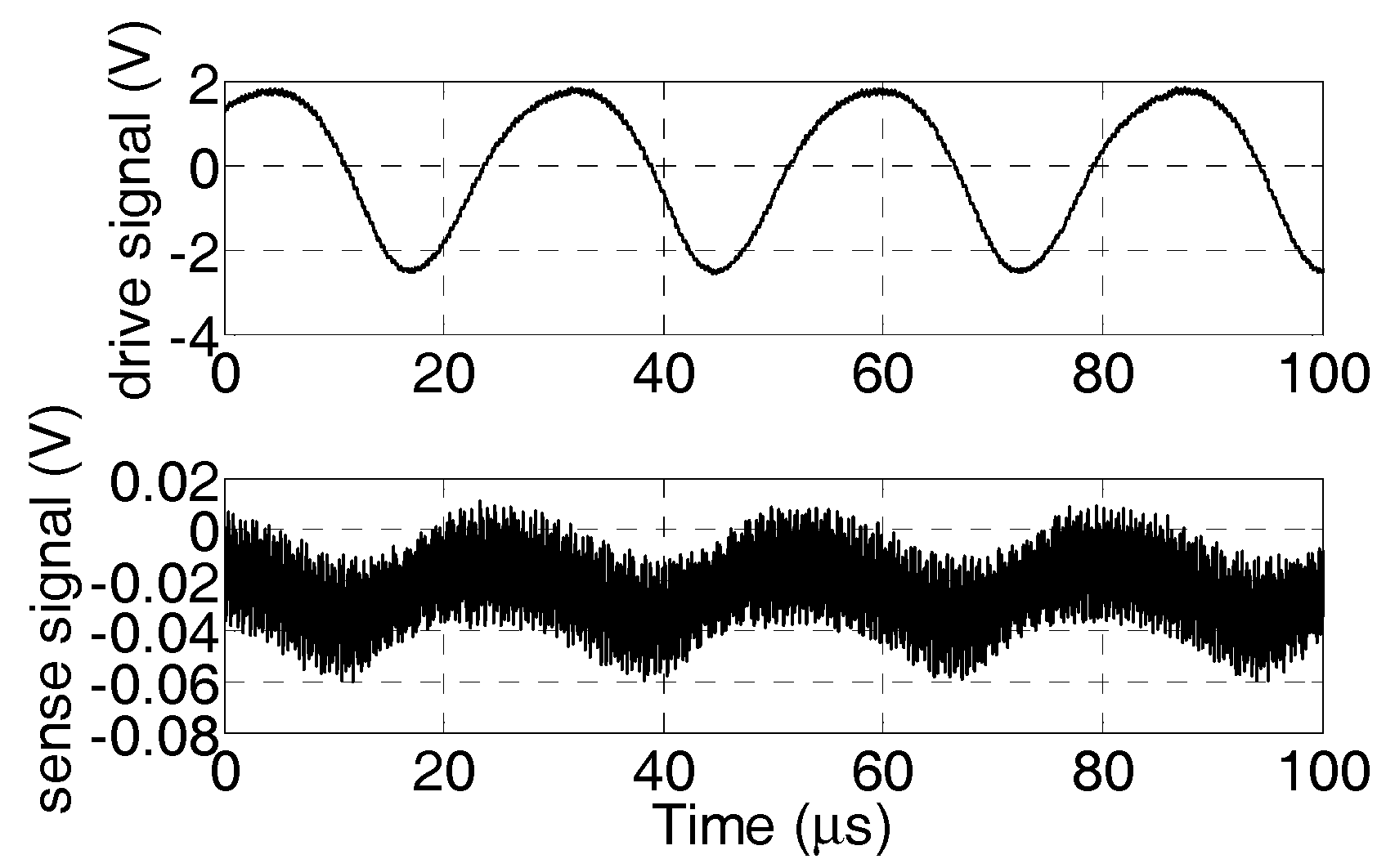
Figure 8.
Bi-axial laser projection by the CMOS MEMS scanning mirror.

Publisher’s Note: MDPI stays neutral with regard to jurisdictional claims in published maps and institutional affiliations. |
© 2017 by the authors. Licensee MDPI, Basel, Switzerland. This article is an open access article distributed under the terms and conditions of the Creative Commons Attribution (CC BY) license (https://creativecommons.org/licenses/by/4.0/).
Share and Cite
MDPI and ACS Style
Li, Z.-H.; Lin, Y.-T.; Lu, M.S.-C. An Electromagnetically-Driven Piezoresistively Sensed CMOS MEMS Scanning Mirror for Projection Display. Proceedings 2017, 1, 353. https://doi.org/10.3390/proceedings1040353
AMA Style
Li Z-H, Lin Y-T, Lu MS-C. An Electromagnetically-Driven Piezoresistively Sensed CMOS MEMS Scanning Mirror for Projection Display. Proceedings. 2017; 1(4):353. https://doi.org/10.3390/proceedings1040353
Chicago/Turabian StyleLi, Zhong-He, Yu-Tang Lin, and Michael S.-C. Lu. 2017. "An Electromagnetically-Driven Piezoresistively Sensed CMOS MEMS Scanning Mirror for Projection Display" Proceedings 1, no. 4: 353. https://doi.org/10.3390/proceedings1040353