On-Chip Platform for Slack-Free Carbon Nanotube Resonators †

Micro and Nanosystems, Department of Mechanical and Process Engineering, ETH Zurich, Switzerland
*
Author to whom correspondence should be addressed.
†
Presented at the Eurosensors 2017 Conference, Paris, France, 3–6 September 2017.
Proceedings 2017, 1(4), 374; https://doi.org/10.3390/proceedings1040374
Published: 8 August 2017
(This article belongs to the Proceedings of Proceedings of Eurosensors 2017, Paris, France, 3–6 September 2017)
Abstract
:This work describes an on-chip integrated micro-actuator device for slack-free carbon nanotube (CNT) resonators, improving frequency tunability and Q factor and to study non-linear mode interaction. The device fabricated on SOI wafer with low thermal budget (<600 K) encompasses a restricted symmetrical out-of-plane vibration and a stiff in-plane electro-thermal actuator with a displacement of ~112 nm at 2.7 mW. This corresponds to 5.6% of strain for a 2 μm long suspended carbon nanotube. The in-plane mechanical resonance designed to be far from CNT resonances in MHz regime is measured at 209 kHz. The design is optimized for low power consumption, electrical and thermal isolation and is customized for dry transfer of CNTs.
1. Introduction
Single-walled carbon nanotube resonant sensors have previously been demonstrated as ultra sensitive compared to other NEMS and MEMS based resonant sensors [1,2]. In CNT resonant sensors, both as-grown and dry transferred CNTs over a trench usually have a slack [3] which alters the dynamic behavior of CNT resonators [4]. A nanotube with slack, shows both in-plane and out-of-plane resonances [5] below the fundamental flexural mode. In contrast, it has been shown that reduction of slack increases the resonant frequency up to 20 times more along with an increase in the quality factor [6], both of which are two important parameters for improving the performance of a sensor. Yet only very little work has been reported to eliminate slack. This work presents an on-chip design for potentially slack-free suspended CNTs by axial straining and henceforth minimizing slack dependence and increasing performance of CNT based resonant sensors. Our design is furthermore compared to previously reported work.
2. Modeling and Fabrication
Figure 1 shows the design of a suspended CNT-FET configuration integrated with thermal micro-actuators. The FET architecture was designed to be compatible for dry transfer of CNTs [7] on to the source-drain electrodes. Carbon nanotubes can then be axially elongated and strained by applying a voltage difference across the thermal beams. The Joule heat generated increases the temperature and expands the beam in turn moving one of the two FET electrodes in the direction y as shown. CNTs can be elongated with an experimentally observed breaking strain of up to 5.8% [8]. For 2 μm long resonator, a 5% strain requires a 100 nm elongation. Secondly, the mechanical resonances of the design should not interfere with CNT resonances in MHz regime. Furthermore, the interconnecting beam between FET and actuator should account for thermal and electrical insulation. The mechanical behavior of thermal actuator was modeled by considering a single pair of V-shaped thermal beams (Figure 1-Inset). The displacement of a pair of thermal beams of length l and cross sectional area Ac due to finite temperature increase ∆T is given by [9]
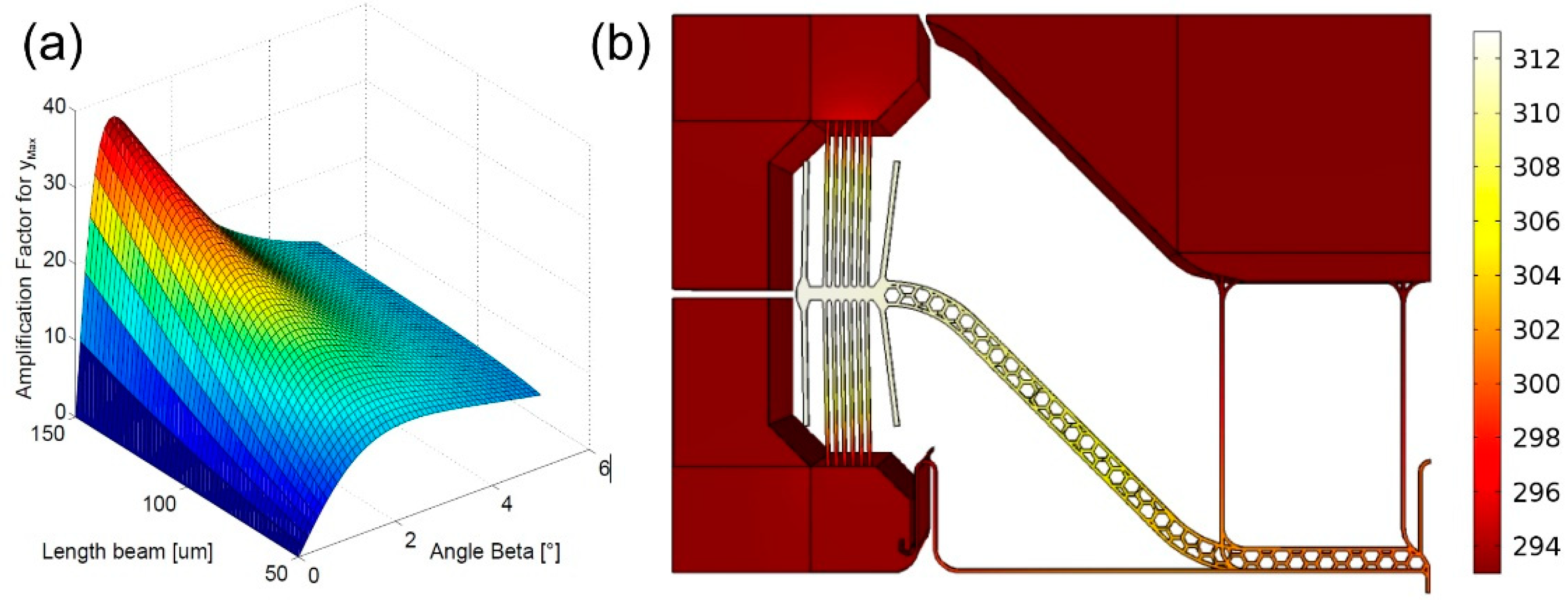
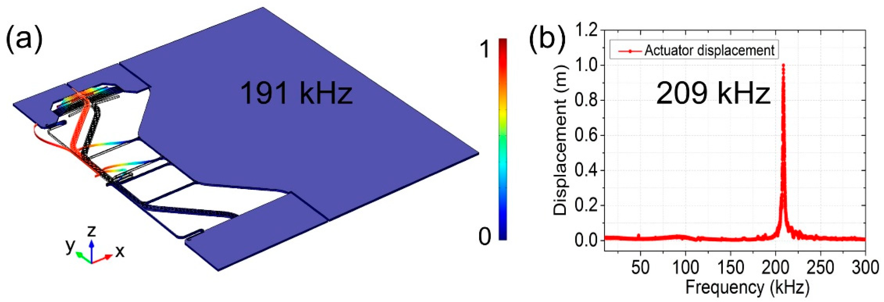
where α is the coefficient of thermal expansion, θ is the beam angle for V-shape thermal actuator, I is the moment of inertia about the out-of-plane z axis and AF is introduced as an amplification factor depending on beam dimension and angle. For a device layer of 5 μm, an optimum angle θ = 1.15° with a beam length of 100 μm were used as shown in Figure 2a. In order to thermally insulate the CNT sensor, the temperature rise ∆T was reduced along the interconnected suspended beam acting as a heat sink. Figure 2b shows the temperature profile for 4.8 mW at 1 V actuator voltage simulated using COMSOL Multiphysics. The mechanical resonances were studied through eigenmode analysis and the first in-plane fundamental mode was found at 191 kHz. The FET S/D electrodes were connected by a U-Beam to avoid out-of plane anti-symmetrical resonances.
The design was fabricated on Silicon-on-Insulator (SOI/300 μm + 1 μm + 5 μm/handle + oxide + device layer) with a low thermal budget of less than 600 K as shown in Figure 3. The suspended FET architecture consists of two Pd coated bottom-gate electrodes in a 275 nm trench depth allowing axial pulling of source/drain electrodes. The 5 μm thick doped-Si actuator is connected to CNT-FET with 325 μm long suspended beam. The Pd is separated from the doped-Si layer by 550 nm SiNx layer (Figure 1) for electrical insulation between the resonator signal and actuator current. Compared to the previous version of polyMUMPs based TEM-compatible design [3], the present work simplifies the process by eliminating the shadow mask. As explained in subsequent sections, the platform is designed for low thermal stress and low power consumption.
3. Measurement and Results
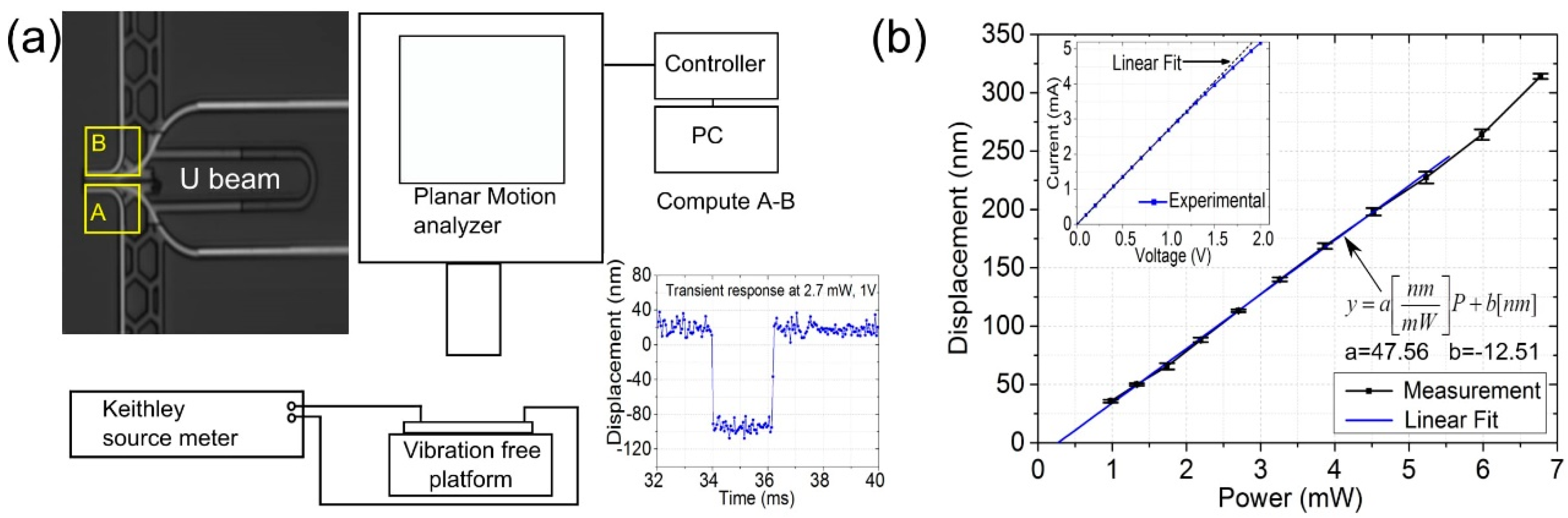
The mechanical behavior of the thermal actuator was measured by planar motion analyzer (Polytec PMA 400) at ambient conditions (Figure 4a) and the relative displacement between the source and drain electrode was extracted by digital imaging. The mechanical response was linear for power < 5.5 mW. The resistance increase due to heating was seen after 5.5 mW at 1.5 V (Figure 4b-Inset). The linear fit suggests the onset of displacement at 0.26 mW at 0.3 V. This could be attributed to beam stiffness and initial residual stress in the actuator beam.
Actuation and recovery time (Figure 4a-Inset) are < 1 ms for 2.7 mW power at 1 V corresponding to 112 nm of displacement. For a 2 μm CNT, this corresponds to 5.6% axial strain and beyond and suitable for CNT straining. The first in-plane eigenfrequency (Figure 5) was measured at 209 kHz by mounting the device on piezo-stage and using white noise excitation.
We expect deviations from the simulated eigenmode study as they did not account for intrinsic stress after fabrication.
4. Discussion and Conclusions
We compare our results to previously reported work for CNT straining as shown in Table 1. The dry transfer compatible design consumes 5 times less power than previous on-chip design in [3] with minimized temperature induced stress and device’s mechanical resonance in kHz region.
Apart from improving and studying CNT resonators, the design can be extended as a platform for other nanoresonators like nanowires, for in-situ tensile and TEM analysis and investigation of strain sensors and gauge factors on a chip level.
Acknowledgments
This work would like to acknowledge clean room facility Binnig and Rohrer Nanotechnology Center (BRNC) at IBM Research, Zurich and FIRST CLA at ETH Zurich for equipment accessibility and useful discussion. We would also like to kindly acknowledge the Swiss National Science Foundation (SNSF) for the funding support.
Conflicts of Interest
The Authors declare no conflict of interest in the reported research results. The founding sponsors had no role in the design of the study; in the collection, analyses, or interpretation of data; in the writing of the manuscript, and in the decision to publish the results.
References
- Moser, J.; Güttinger, J.; Eichler, A.; Esplandiu, M.J.; Liu, D.E.; Dykman, M.I.; Bachtold, A. Ultrasensitive force detection with a nanotube mechanical resonator. Nat. Nanotechnol. 2013, 8, 493–496. [Google Scholar] [CrossRef]
- Chaste, J.; Eichler, A.; Moser, J.; Ceballos, G.; Rurali, R.; Bachtold, A. A nanomechanical mass sensor with yoctogram resolution. Nat. Nanotechnol. 2012, 7, 301–304. [Google Scholar] [CrossRef]
- Truax, S.; Lee, S.W.; Muoth, M.; Hierold, C. Axially tunable carbon nanotube resonators using co-integrated microactuators. Nano Lett. 2014, 14, 6092–6096. [Google Scholar] [CrossRef]
- Ouakad, H.M.; Younis, M.I. Dynamic response of slacked single-walled carbon nanotube resonators. Nonlinear Dyn. 2012, 67, 1419–1436. [Google Scholar] [CrossRef]
- Ning, Z.; Fu, M.Q.; Wu, G.; Qiu, C.; Shu, J.; Guo, Y.; Wei, X.; Gao, S.; Chen, Q. Remarkable influence of slack on the vibration of a single-walled carbon nanotube resonator. Nanoscale 2016, 8, 8658–8665. [Google Scholar] [CrossRef] [PubMed]
- Ning, Z.; Fu, M.Q.; Shi, T.W.; Guo, Y.; Wei, X.; Gao, S.; Chen, Q. Transversally and axially tunable carbon nanotube resonators in Situ fabricated and studied inside a scanning electron microscope. Nano Lett. 2014, 14, 1221–1227. [Google Scholar] [CrossRef] [PubMed]
- Muoth, M.; Hierold, C. Transfer of carbon nanotubes onto micro actuators for hysteresis-free transistors at low thermal budget. In Proceedings of the IEEE 25th International Conference on MEMS, Paris, France, 29 January–2 February 2012; pp. 1352–1355. [Google Scholar]
- Walters, D.A.; Ericson, L.M.; Casavant, M.J.; Liu, J.; Colbert, D.T.; Smith, K.A.; Smalley, R.E. Elastic strain of freely suspended single-wall carbon nanotube ropes. Appl. Phys. Lett. 1999, 74, 3803–3805. [Google Scholar] [CrossRef]
- Zhu, Y.; Espinosa, H.D. An electromechanical material testing system for in situ electron microscopy and applications. Proc. Natl Acad. Sci. USA 2005, 102, 14503–14508. [Google Scholar] [CrossRef] [PubMed]
- Wei, X.; Chen, Q.; Xu, S.; Peng, L.; Zuo, J. Beam to string transition of vibrating carbon nanotubes under axial tension. Adv. Funct. Mater. 2009, 19, 1753–1758. [Google Scholar] [CrossRef]
Figure 1.
The Design configuration consisting of a thermal actuator integrated with suspends CNT FET architecture through a heat sink beam. Inset-Schematic of a pair of V-shaped beams with stiffness kT subjected to an axial movement due to an average increase in temperature.
Figure 1.
The Design configuration consisting of a thermal actuator integrated with suspends CNT FET architecture through a heat sink beam. Inset-Schematic of a pair of V-shaped beams with stiffness kT subjected to an axial movement due to an average increase in temperature.

Figure 2.
(a) Amplification factor for a single thermal beam as a function of beam angle and beam length; (b) Temperature profile (in Kelvin) along the device for 4.8 mW at 1 V actuator voltage.
Figure 2.
(a) Amplification factor for a single thermal beam as a function of beam angle and beam length; (b) Temperature profile (in Kelvin) along the device for 4.8 mW at 1 V actuator voltage.

Figure 3.
SEM (a,b) and optical image (c) of suspended CNT-FET with integrated on-chip thermal actuator.
Figure 3.
SEM (a,b) and optical image (c) of suspended CNT-FET with integrated on-chip thermal actuator.

Figure 4.
(a) Planar motion analyzer for measuring displacement between drain (B) and source (A) electrode; (b) Actuator displacement vs. power. The error bar results from averaging of the transient response. (Inset-b) Measured voltage vs. current. The resistance increases after 1.5 V due to joule heating.

Figure 5.
(a) First in-plane eigenmode (displacement normalized to 1) simulated in COMSOL; (b) First in-plane resonance measured using LDV by tilting the sample (~90°) mounted on a piezo stage.
Figure 5.
(a) First in-plane eigenmode (displacement normalized to 1) simulated in COMSOL; (b) First in-plane resonance measured using LDV by tilting the sample (~90°) mounted on a piezo stage.


Table 1.
Previously reported work for CNT straining.
| Ref. | Design | CNT Placement | Power @ 100 nm |
|---|---|---|---|
| [6] | PC controlled piezo-SEM stage | 3 probe pick-up-drop | - |
| [10] | AFM cantilever | 3 nanoprobe system | - |
| [9] | On-chip thermal actuator | Probe nanomanipulation | ~28 mW |
| [3] | On-chip thermal actuator | As grown and dry transfer | ~10 mW |
| This work | On-chip thermal actuator | Dry-transfer | 2.7 mW |
Publisher’s Note: MDPI stays neutral with regard to jurisdictional claims in published maps and institutional affiliations. |
© 2017 by the authors. Licensee MDPI, Basel, Switzerland. This article is an open access article distributed under the terms and conditions of the Creative Commons Attribution (CC BY) license (https://creativecommons.org/licenses/by/4.0/).
Share and Cite
MDPI and ACS Style
Kumar, L.; Jenni, L.V.; Roman, C.I.; Hierold, C. On-Chip Platform for Slack-Free Carbon Nanotube Resonators. Proceedings 2017, 1, 374. https://doi.org/10.3390/proceedings1040374
AMA Style
Kumar L, Jenni LV, Roman CI, Hierold C. On-Chip Platform for Slack-Free Carbon Nanotube Resonators. Proceedings. 2017; 1(4):374. https://doi.org/10.3390/proceedings1040374
Chicago/Turabian StyleKumar, Lalit, Laura Vera Jenni, Cosmin Ioan Roman, and Christofer Hierold. 2017. "On-Chip Platform for Slack-Free Carbon Nanotube Resonators" Proceedings 1, no. 4: 374. https://doi.org/10.3390/proceedings1040374