Gas Sensing Approaches Based on WO3 Nanowire-Back Gated Devices †


MINOS/EMaS, Universitat Rovira i Virgili, Av. Paìsos Catalans 26, 43007 Tarragona, Spain
*
Author to whom correspondence should be addressed.
†
Presented at the Eurosensors 2017 Conference, Paris, France, 3–6 September 2017.
Proceedings 2017, 1(4), 437; https://doi.org/10.3390/proceedings1040437
Published: 9 August 2017
(This article belongs to the Proceedings of Proceedings of Eurosensors 2017, Paris, France, 3–6 September 2017)
Abstract
:This paper present a new design and configuration of metal oxide gas sensor based on back-gated device that can operate at low temperature. Gold electrodes patterned onto an oxidized, heavily doped, p-type silicon substrate were designed and fabricated at a wafer level. The Au—electrodes were used as source—drain metal contacts and a third gate electrode was connected from the backside of the substrate. Tungsten oxide nanowires decorated with Pt-nanoparticles were directly grown employing aerosol assisted-CVD (AA-CVD) on top of the electrode area. Gas sensing properties of the back-gated device in the presence of air and hydrogen gas reveals characteristic response modulated by the applied gate potential at room temperature. It was found that the IDS-VGS plot illustrates characteristic field effect transistor with an inherent adsorptive surface electron transfer of the nanowires accompanied with the applied gate potential induced charge transfer. These counter-acting mechanisms might persuade for the application of back-gated device as a promising n-channel metal oxide gas sensor operating at low temperature or even room temperature.
1. Introduction
Gas sensors based on single crystalline metal oxide nanostructures (SMOx) offer many advantages in sensor performance such as high stability at typical operating temperatures, high surface to volume ratio, and tailored surface chemistry via functionalization [1,2,3]. At a given high operating temperature, the surface of the sensing material gives rise to high concentration of adsorbed oxygen species, which modulates the electron density at the surface and its electronic state. To this end, there has been much progress in the fabrication, and integration of different single crystalline SMOx nanostructures decorated with metal nanoparticles for gas sensing at low temperature; as well as optimizing the minimum power consumption of such devices while maintaining high sensor performance and stability [4]. Recently, highly sensitive gas sensors based on nanoparticle decorated WO3 nanowires for the detection of various gases at low temperature have been explored [5,6].
However, some barriers to employ less power consuming resistive SMOx sensor platforms are still to be overcome. Especially, achieving SMOx devices able to work at relatively low temperature are much sought for. Here we describe a simple back-gated FET device based on Pt functionalized WO3 nanowires for gas sensing at low temperature. The hybrid nanostructure, Pt/WO3 deposited onto the electrode area employing single step aerosol assisted CVD (AA-CVD), was considered as an active sensing material. The device I-V curve and its sensing property to H2 gas at a constant source-drain potential and sweeping gate potential has been investigated at room temperature.
2. Materials and Methods
A 2 inch wafer, heavily p-doped Si<100> (10−3 Ωcm) with 300 µm thickness and 1 µm oxide layer was obtained from Silicon materials, Germany. Electrode design and clean room processes were employed at wafer level following microfabrication procedures including reactive ion etching, sputtering, nanolithography, and wet chemical etching to define the source-drain contact electrodes as well as gate electrode. Schematic top view of the interdigitated Au-electrodes and the corresponding back gated electrode configuration are shown in Figure 1a,b.
Tungsten hexacarbonyl (W(CO)6) powder, chloroplatinic acid hydrate (H2PtCl6·xH2O), acetone and methanol were obtained from Sigma Aldrich (Spain) as a metal precursors and solvents, respectively. Pt-nanoparticle decorated WO3 nanowires were co-deposited directly onto the electrode area in a single step aerosol assisted–CVD (AA-CVD). Prior to the deposition of the nanowires, the substrate was heated to a temperature of 380 °C, and followed by the transfer of ultrafine aerosols to the heated substrate by N2 carrier gas at a flow rate of 0.5 L/min [5,7]. Surface morphology images were taken using Scanning Electron Microscopy (ESEM) with FEI Quanta 60 and Tunneling Electron Microscopy with JOEL model 1011 equipment.
Gas sensing property of the back-gated FET device was examined towards calibrated 500 ppm H2 gas under a constant total gas flow of 200 sccm. Mass flow controllers (Bronkhorst hi-tech 7.03.241), Keysight precision source meter (model B2902A) and Keysight data acquisition equipment (model 34972A) interfaced with a custom made LabVIEW program were used for gas flow calibration and device electrical characterization, respectively.
3. Results and Discussion
3.1. Material Characterizatiion of Pt/WO3 Nanowires
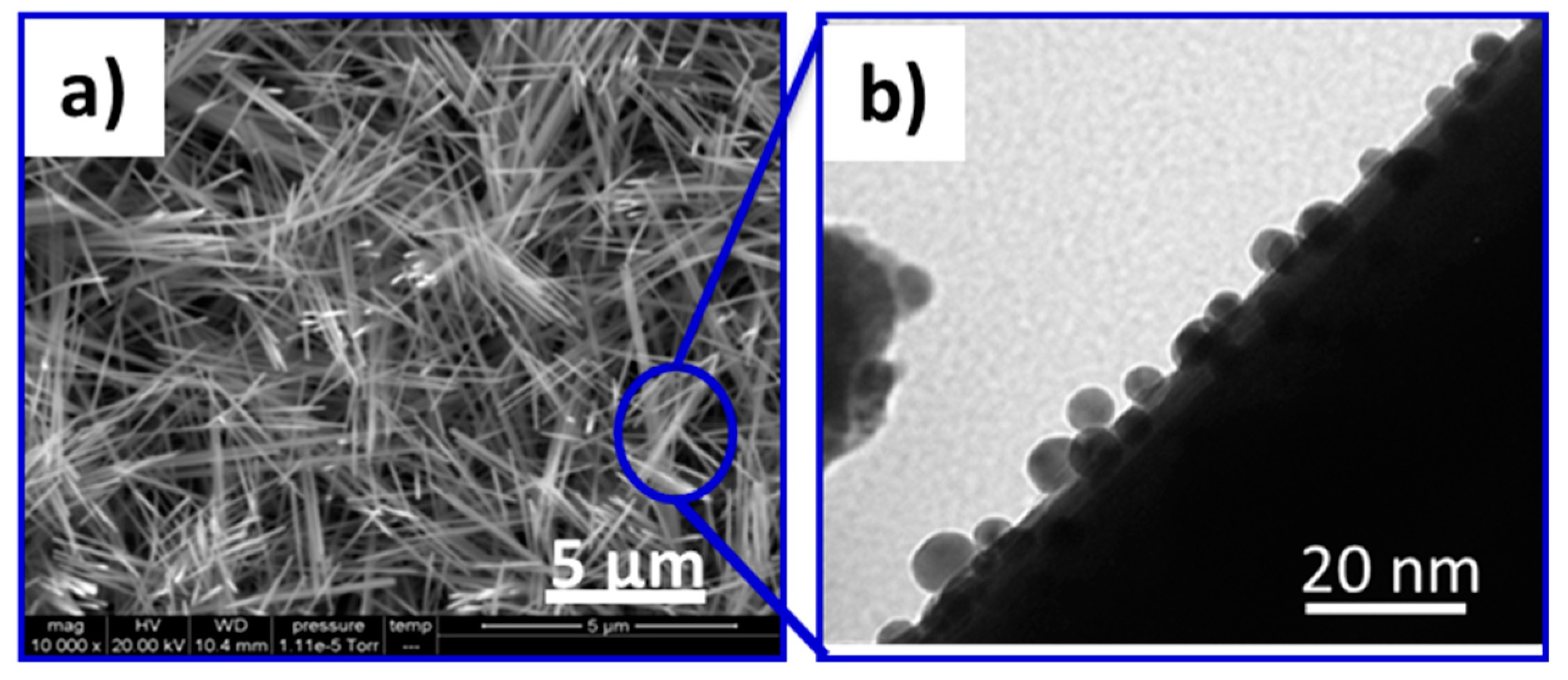
The as-deposited hybrid nanostructures exhibit strong adherence to the substrate with a dark blue color right after deposition indicating the presence of metal oxide structure. A light white color observed, after annealing at 450 °C for 2 h in air, illustrates the presence of PtO onto a slightly sub-stoichiometric tungsten oxide [8]. SEM images of the film show a high density of nonaligned needle-like nanowires with uniform diameters near 120 nm, Figure 2a. TEM images of the as-deposited film clearly depicts randomly distributed Pt-nanoparticles on the surface the nanowires, Figure 2b.
3.2. Gas Sensing Property
To assess the electrical characteristics of the device, a constant voltage (VDS = 1 V) was applied between the source and drain electrodes. Biasing the gate substrate therefore induces an inverted conduction channel at the Si-SiO2 interface thereby producing a complete IDS-VGS curve. A simultaneous depletion and accumulation of electron-hole takes place at the interface as a result of substrate gate biasing between −3 V to +3 V (sweep rate ~100 mV/s). We therefore took this advantage to modulate the surface potential of the n-type Pt/WO3 nanowires to sensitize its chemical and electronic property without thermal heating. Figure 3a displays characteristic gas sensing property of the sensor in the presence of dry synthetic air and 500 ppm H2 gas at room temperature. The inset (Figure 3a) shows a positive current decrease when the sensor is exposed to the H2 gas and a positive gate potential, while a decrease in current was observed for negative bias gate potential (Figure 3c).
We found no current transfer between the source and drain at VGS = 1 and this might be related with the threshold potential corresponding to the onset of the charge transfer between source-drain with respect to the gate driven depletion layer. It is thought that some parasitic leakage current might occur through the oxide layer into the substrate. This might be due to the heating of the substrate in the deposition process of the nanowires in such a way the nanowires could penetrate through the dielectric oxide layer. It is noted that the IDS values were higher when the device is operating with gate biasing in dynamic mode. Figure 3d shows sensor response towards to synthetic air and 500 ppm H2 gas exposures while the device was operating at constant gate potential, VGS = 3 V and VDS = 1 V. It is thought that the decrease in transfer current might be related to the trade-off between counteracting adsorbed surface electron transfer and gate potential induced charge transfer.
4. Conclusions
A three contact electrode sensor device with a back-gated configuration was designed and fabricated at wafer level. Pt nanoparticle decorated WO3 were grown onto the electrode area employing single step AA-CVD. The charge transfer between source-drain electrodes, IDS, at constant VDS was characterized while sweeping the gate potential between −3 V to 3 V. The IDS vs VGS plot illustrates characteristic field effect transistor and IDS changes when the device was exposed to dry air and H2 gas. The surface adsorptive property the sensing material was modulated with the applied gate potential. The results have shown that this simple back-gated device is very promising to be employed as an n-channel metal oxide gas sensor operating at low temperatures or even room temperature.
Acknowledgments
This work is funded by MINECO under grant TEC2015-71663-R. E.L. is supported by ICREA under the ICREA Academia Award. T.G.W acknowledges a FPI predoctoral fellowship from MINECO under grant No. BES-2013-063682.
Conflicts of Interest
The authors declare no conflict of interest.
References
- Kolakov, A. Some recent trends in fabrication, functionalization, and characterization of metal oxide gas sensors. Int. J. Nanotechnol. 2008, 5, 12–14. [Google Scholar]
- Comini, E.; Barrato, C.; Concin, I.; Fagila, G.; Falasconi, M.; Ferroni, M.; Galstyan, V.; Gobbi, E.; Ponzoni, A.; Vomiero, A.; et al. Metal oxide nanoscience and nanotechnology for chemical sensors. Sens. Actuators B Chem. 2013, 179, 3–20. [Google Scholar] [CrossRef]
- Annanouch, F.E.; Haddi, Z.; Vallejos, S.; Umek, P.; Guttmann, P.; Bittencourt, C.; Llobet, E. Aerosol-assisted CVD-grown WO3 nanoneedles decorated with copper oxide nanoparticles for the selective and humidity-resilient detection of H2S. ACS Appl. Mater. Interfaces 2015, 7, 6842–6851. [Google Scholar] [CrossRef] [PubMed]
- Kolmakov, A.; Chen, X.; Moskovits, M. Functionalizing nanowires with catalytic nanoparticles for gas sensing application. J. Nanosci. Nanotechnol. 2008, 8, 111–121. [Google Scholar] [CrossRef] [PubMed]
- Annanouch, F.E.; Haddi, Z.; Ling, M.; Vallejos, S.; Shujah, T.; Umek, P.; Bittencourt, C.; Blackman, C.; Llobet, E. Aerosol-Assisted CVD-grown PdO nanoparticle-decorated Tungsten Oxide nanoneedles extremely sensitive to Hydrogen. ACS Appl. Mater. Interfaces 2016, 8, 10413–10421. [Google Scholar] [CrossRef] [PubMed]
- Vallejos, S.; Stoycheva, T.; Annanouch, F.E.; Llobet, E.; Umek, P.; Figueras, E.; Canè, C.; Gràcia, I.; Blackman, C. Microsensors based on Pt-nanoparticle functionalised tungsten oxide nanoneedles for monitoring hydrogen sulfide. RSC Adv. 2014, 4, 1489–1495. [Google Scholar] [CrossRef]
- Vallejos, S.; Umek, P.; Stoycheva, T.; Annanouch, F.; Llobet, E.; Correig, X.; De Marco, P.; Bittencourt, C.; Blackman, C. Single-step deposition of Au- and Pt-nanoparticle functionalized tungsten oxide nanoneedles synthesized via aerosol-assisted CVD, and used for fabrication of selective gas microsensor arrays. Adv. Funct. Mater. 2013, 23, 1313–1322. [Google Scholar] [CrossRef]
- Annanouch, F.E.; Vallejos, S.; Stoycheva, T.; Blackman, C.; Llobet, E. Aerosol assisted chemical vapour deposition of gas sensitive nanomaterials. Thin Solid Films 2013, 548, 703–709. [Google Scholar] [CrossRef]
Figure 1.
(a) 15 μm gapped interdigitated gold electrodes for source-drain contacts; (b) back-gated sensor configuration with back gate electrode and active sensing material between source-drain electrodes.
Figure 1.
(a) 15 μm gapped interdigitated gold electrodes for source-drain contacts; (b) back-gated sensor configuration with back gate electrode and active sensing material between source-drain electrodes.

Figure 2.
(a) SEM images of the as-deposited films of Pt-nanoparticles decorated tungsten oxide nanoneedle-like nanowires (Pt/WO3); (b) PtNPs on the surface of nanowires.
Figure 2.
(a) SEM images of the as-deposited films of Pt-nanoparticles decorated tungsten oxide nanoneedle-like nanowires (Pt/WO3); (b) PtNPs on the surface of nanowires.

Figure 3.
(a) IDS vs VGS sensor response of back-Gated FET sensor under synthetic air (open square) and 500 ppm H2 (triangle) gas exposures, at constant VDS = 1 V; the insets (b,c) shows the sensor responses for VGS = 3 V to 1 V and 1 V to −3 V, respectively; (d) sensor response to 500 ppm H2 gas exposure extracted at constant, VGS = 3 V and VDS = 1 V.

Publisher’s Note: MDPI stays neutral with regard to jurisdictional claims in published maps and institutional affiliations. |
© 2017 by the authors. Licensee MDPI, Basel, Switzerland. This article is an open access article distributed under the terms and conditions of the Creative Commons Attribution (CC BY) license (https://creativecommons.org/licenses/by/4.0/).
Share and Cite
MDPI and ACS Style
Welearegay, T.G.; Calavia, R.; Ionescu, R.; Llobet, E. Gas Sensing Approaches Based on WO3 Nanowire-Back Gated Devices. Proceedings 2017, 1, 437. https://doi.org/10.3390/proceedings1040437
AMA Style
Welearegay TG, Calavia R, Ionescu R, Llobet E. Gas Sensing Approaches Based on WO3 Nanowire-Back Gated Devices. Proceedings. 2017; 1(4):437. https://doi.org/10.3390/proceedings1040437
Chicago/Turabian StyleWelearegay, Tesfalem G., Raul Calavia, Radu Ionescu, and Eduard Llobet. 2017. "Gas Sensing Approaches Based on WO3 Nanowire-Back Gated Devices" Proceedings 1, no. 4: 437. https://doi.org/10.3390/proceedings1040437