Proceeding Paper

Investigation of the Salt Concentration Dependence of Water-Gated Field Effect Transistors (WG-FET) Using 16-nm-Thick Single Crystalline Si Film †

Department of Electrical & Electronics Engineering, Bogazici University, 34342 Istanbul, Turkey
*
Author to whom correspondence should be addressed.
Presented at the Eurosensors 2017 Conference, Paris, France, 3–6 September 2017.
Proceedings 2017, 1(4), 486; https://doi.org/10.3390/proceedings1040486
Published: 9 August 2017
(This article belongs to the Proceedings of Proceedings of Eurosensors 2017, Paris, France, 3–6 September 2017)

Abstract

:
This paper presents the effect of NaCl concentration on the operation of a water-gated field effect transistor (WG-FET) that uses 16-nm-thick single crystalline silicon (Si) film. In WG-FET, electrical double layer (EDL) formed at the water/silicon interface behaves as gate dielectric and this fluidic interface makes WG-FET a suitable device for sensing applications. Characteristics of EDL and the threshold voltage of WG-FET depend on the molarity of solution. Increasing the molarity of NaCl solution from 0.5 to 65 mM changes the threshold voltage from 360 to 465 mV. Accordingly, drain current of the WG-FET device changes with NaCl concentration.

1. Introduction

Water-gated field effect transistors (WG-FET) that use 16-nm-thick mono-Si films as channel layers promise a new platform where chemical/biological sensors and their read-out circuits can be integrated together. By using electrical double layer capacitance (EDLC) as gate insulator, high channel control can be achieved at low gate voltages with cheap and easy device fabrication. Ultra-thin and high mobility characteristics of the channel layer result in high surface sensitivity in sensor applications and on-site amplification in their read-out circuits.
Applied gate potential in this device induces a voltage across the EDL capacitance, which causes accumulation of holes on the surface of p-type thin Si film as shown in Figure 1. This accumulation type device contains no p-n junctions, which reduces the fabrication cost and light sensitivity. Otherwise, electron-hole pairs can be created in these junctions in the presence of light and introduce noise to the system. IDS current of the WG-FET is determined by EDL capacitance and the threshold voltage. Similar to Si nanowire FETs [1] and ion-sensitive FETs (ISFET) [2], both threshold voltage and EDL capacitance, hence IDS, change with pH and the ion concentration of the solution as given by equations in Section 3. In this work, the effect of NaCl concentration on the operation of these WG-FETs is investigated for the first time.

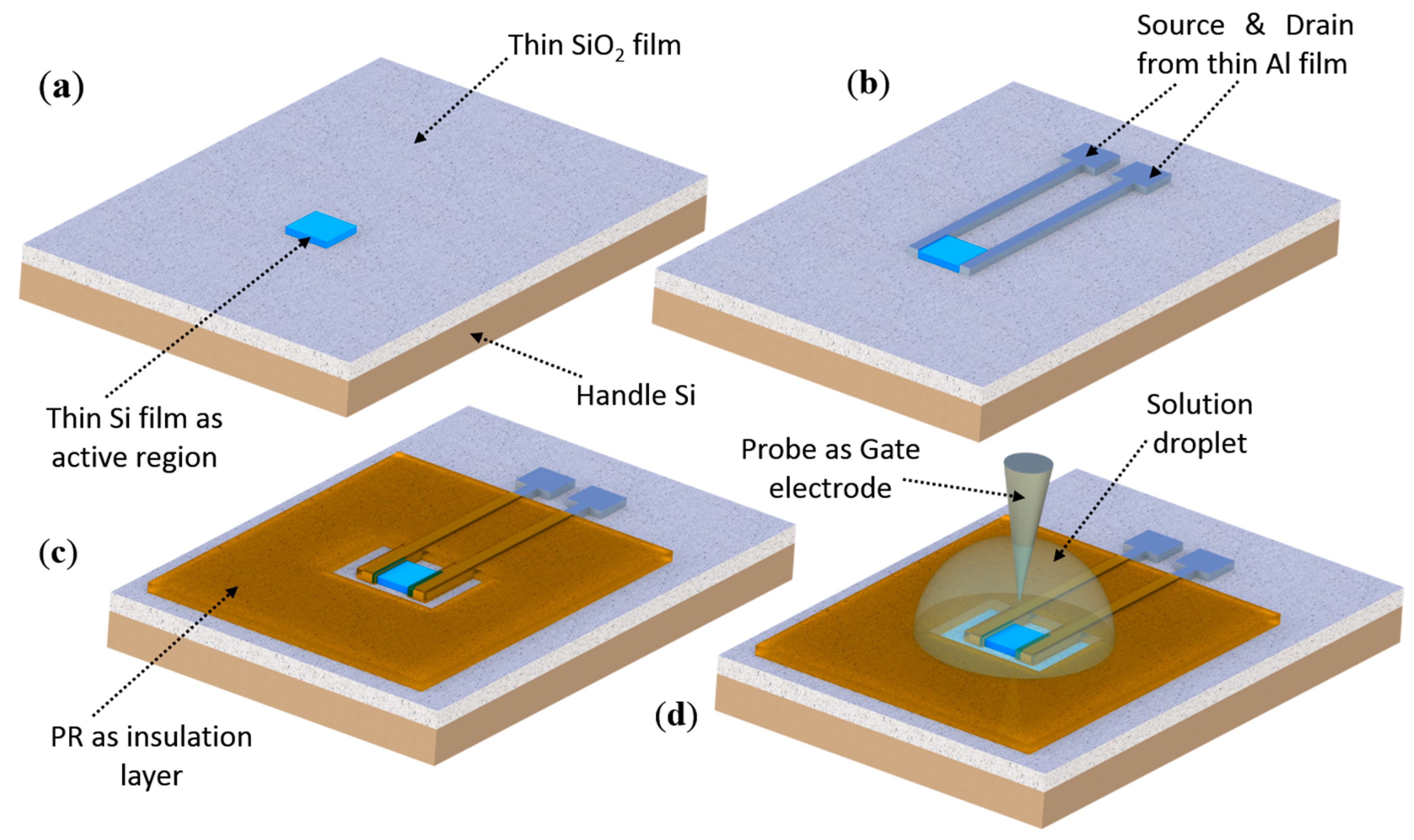
2. Materials and Methods

WG-FET device is fabricated using a silicon-on-insulator (SOI) wafer. Fabrication steps are illustrated in Figure 2. First, 16 nm thick Si device layer is patterned to form the active region of the transistor on top of the 145-nm-thick SiO2. Then, 200-nm-thick aluminum (Al) is thermally evaporated and patterned to build source and drain electrodes. After thermal annealing at 500 °C, ohmic contacts are obtained between Al and Si films. SiO2 in the field regions are insulated with photoresist (PR) for repeatability enhancement [3]. Source and drain electrodes are also insulated to prevent galvanic corrosion of Al in NaCl solution.
A solution droplet is placed on top of the active region and a probe is immersed as the gate electrode. A device under test is shown in Figure 3. Contact pads are connected to the wires using silver epoxy paste.

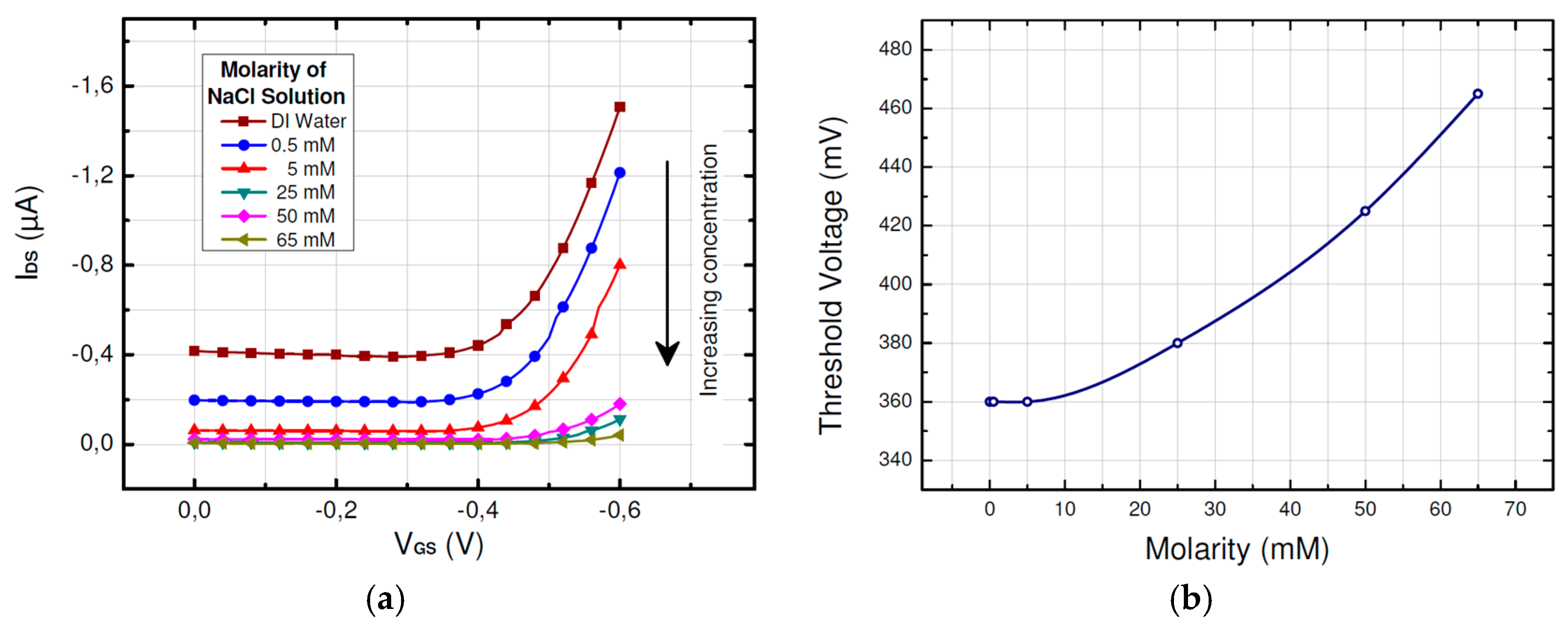
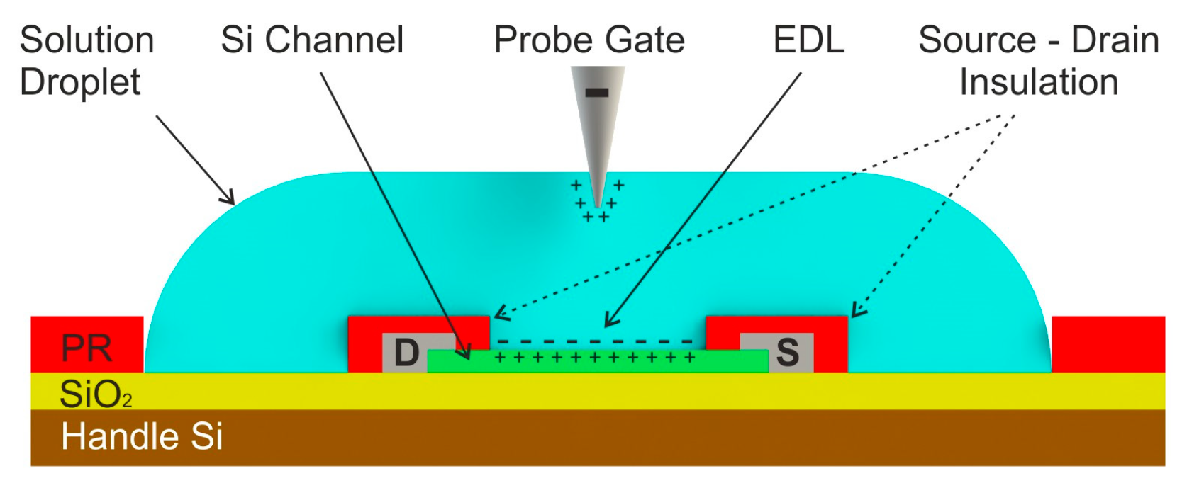
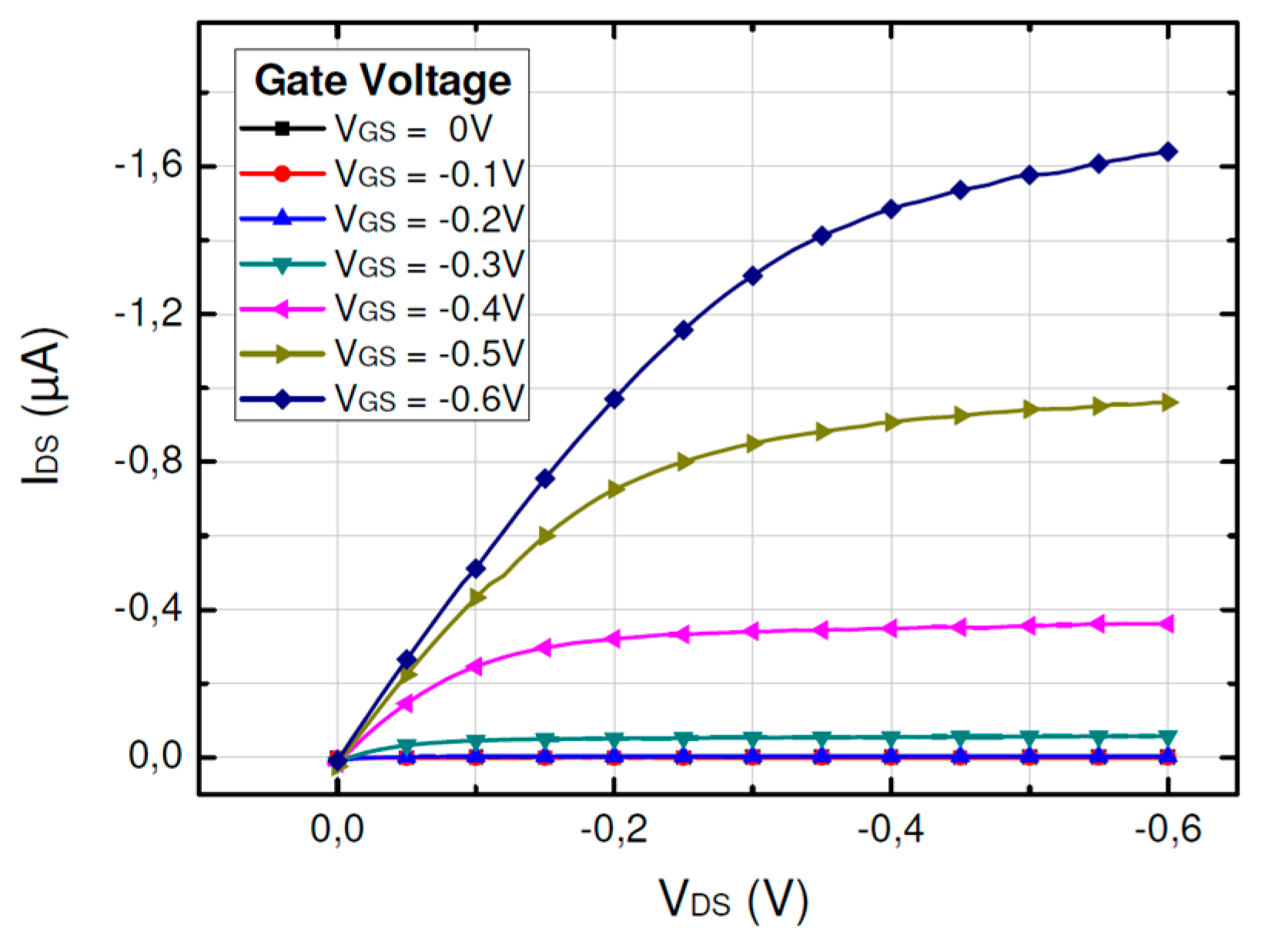
3. Results and Discussion

Characteristic IDS-VDS curves of the WG-FET with de-ionized (DI) water are presented in Figure 4, showing the typical transistor characteristics of the WG-FET used in this work. Applied voltages are limited to 0.6 V to eliminate any electrochemical reaction in NaCl solution, which keeps EDL operations in non-Faradaic region. Transfer characteristic curves of the transistor (IDS-VGS) are measured at VDS = VDD for different molarities, as shown in Figure 5a. Increasing NaCl concentration reduces the on-current of the WG-FET.
Threshold voltages for each NaCl molarity are extracted from the IDS-VGS curves and plotted in Figure 5b. These results can be explained as below with the complex dependence of EDL capacitance and threshold voltage on the ion concentration of the solution.
The WG-FET contains two EDL capacitances, one at the surface of probe gate electrode and the other on active channel. These are connected in series, hence when a potential is applied to gate electrode, only some portion of it drops across the EDL of the active channel, which we refer as the effective gate voltage VGS_eff. The current passing through the WG-FET in the saturation region can be characterized by the equation
I DS = 1 2 W L μ p C edl ( V GS _ eff V T ) 2 ,
where W is the channel width, L is the channel length, µp is the mobility of holes in thin-Si, Cedl is the EDL capacitance on the active channel and VT is the threshold voltage. Cedl is a function of ion concentration. VT depends on both ion concentration and pH as shown in Equations (2)–(7). These complex dependences explain the change of the WG-FET current with different solutions. EDL capacitance can be given as [4]
C edl = 2 z 2 q 2 ε ε 0 n 0 kT cos h ( zq Ψ 0 2 kT ) ,
where z is the signed charge of ion, q is the unit charge, ε is the relative permittivity of the solution, ε0 is the permittivity of air, n0 is the number concentration of ion, k is the Boltzmann’s constant, T is absolute temperature and Ψ0 is the electrostatic potential at the surface with respect to bulk solution. This equation simplifies to Equation (3) for dilute aqueous solutions of NaCl at 25 °C where |z| = 1 [4].
C edl = 228   I 0 cosh ( 19.5 Ψ 0 ) ,
where I0 is the ion concentration. Threshold voltage of WG-FET can be expressed as [2]
V T = Ψ bulk Ψ 0 + χ sol ϕ Si q + Q acc C edl
where Ψbulk is the potential of the bulk solution, χsol is the surface dipole potential, ϕSi is the work function of Si and Qacc is the accumulation charge density. The change of the surface potential Ψ0 with respect to the bulk pH is given in Equation (5) [5].
Δ Ψ 0 = Δ pH B   2.3 kT q α   ,
where α is a dimensionless sensitivity parameter varying between 0 and 1, which is [5]
α = ( 2.3 kTC edl q 2 β int + 1 ) 1
where βint is the intrinsic buffer capacity given as [5]
β int = 2.3 a H s + N s K b a H s + 2 + 4 K a K b a H s + + K a K b 2 ( K a K b + K b a H s + + a H s + 2 ) 2
where aHs+ is the activity of H+ at the active silicon layer surface related to the bulk activity, NS is the number of sites per unit area, Ka and Kb are dimensionless dissociation constants.
Our results can be explained with the complex dependence of EDL capacitance and threshold voltage on the ion concentration of the solution as discussed above [4]. The changes in the threshold voltages of our devices with NaCl molarity agree with the study of Bergveld on the effect of NaCl concentration on ISFETs, which are depletion/inversion mode bulk Si devices with large reference electrodes, and have SiO2 insulation [2].

4. Conclusions

It is concluded that concentration of NaCl solution used in WG-FET effects its characteristics by changing threshold voltage and EDL capacitance on the surface of thin Si film. WG-FETs can be both chemical/biological sensors and transistors, leading to an integrated platform where sensors and their read-out circuits are together.

Acknowledgments

This work is supported by Scientific and Technological Research Council of Turkey (TUBITAK) under project EEEAG 114R080.

Conflicts of Interest

The authors declare no conflict of interest.

References

  1. Chen, Y.; Wang, X.; Erramilli, S.; Mohanty, P.; Kalinowski, A. Silicon-based nanoelectronic field-effect pH sensor with local gate control. Appl. Phys. Lett. 2006, 89, 223512. [Google Scholar] [CrossRef]
  2. Bergveld, P. Thirty years of ISFETOLOGY: What happened in the past 30 years and what may happen in the next 30 years. Sens. Actuators B Chem. 2003, 88, 1–20. [Google Scholar] [CrossRef]
  3. Sonmez, B.G.; Ertop, O.; Mutlu, S. Improved repeatability in planar water-gated field effect transistor (WG-FET) with 16-nm-thick single crystalline Si film. Procedia Eng. 2016, 168, 1739–1742. [Google Scholar] [CrossRef]
  4. Bard, A.J.; Faulkner, L.R. Double-Layer Structure and Adsorption. In Electrochemical Methods Fundamentals and Applications, 2nd ed.; John Wiley & Sons, Inc.: New York, NY, USA, 2001; pp. 534–579. [Google Scholar]
  5. Van Hal, R.E.G.; Eijkel, J.C.T.; Bergveld, P. A novel description of ISFET sensitivity with the buffer capacity and double-layer capacitance as key parameters. Sens. Actuators B Chem. 1995, 24–25, 201–205. [Google Scholar] [CrossRef]
Figure 1. Operation principle of the WG-FET device.
Proceedings 01 00486 g001
Figure 2. Fabrication steps of WG-FET: (a) Wet etching of thin film silicon to pattern the active region; (b) Thermal evaporation and patterning of 200-nm-thick Al film as drain and source electrodes; (c) Spin-coating and patterning of photoresist (PR) layer as insulation for the SiO2 film and source & drain electrodes; (d) Placement of the solution droplet and immersion of the probe gate electrode.
Proceedings 01 00486 g002
Figure 3. Device under test.
Proceedings 01 00486 g003
Figure 4. IDS vs. VDS graph of the WG-FET for various VGS voltages with DI-Water as the water droplet.
Proceedings 01 00486 g004
Figure 5. IDS vs. VGS graphs of WG-FET for various NaCl molarities of the solution droplet (a); Threshold voltage of WG-FET vs. molarity of the NaCl solution (b).
Proceedings 01 00486 g005
Publisher’s Note: MDPI stays neutral with regard to jurisdictional claims in published maps and institutional affiliations.

