Integrated SiGe Detectors for Si Photonic Sensor Platforms †
by
Grégory Pandraud
1,*, 
Silvana Milosavljevic
1,
Amir Sammak
2,
Matteo Cherchi
3,
Aleksandar Jovic
4 and
Pasqualina Sarro
4 1
Else Kooi Laboratory, TU Delft, Feldmannweg 17, 2628 CT, Delft, The Netherlands
2
Qutech, TU Delft, Van der Waalsweg 122, 2628, Delft, The Netherlands
3
VTT Technical Research Center of Finland, P.O. Box 1000, FI-02044 VTT, Finland, Espoo, Finland
4
Electronic Components Technology and Materials, TU Delft, Mekelweg 4, 2628 CD, Delft, The Netherlands
*
Author to whom correspondence should be addressed.
†
Presented at the Eurosensors 2017 Conference, Paris, France, 3–6 September 2017.
Proceedings 2017, 1(4), 559; https://doi.org/10.3390/proceedings1040559
Published: 11 August 2017
(This article belongs to the Proceedings of Proceedings of Eurosensors 2017, Paris, France, 3–6 September 2017)
Abstract
:In this work, we present the results of integrated Ge detectors grown on a Si photonic platform for sensing applications. The detectors are fabricated on a passive photonic circuit for maximum coupling efficiency. Measurement results at 1300 nm wavelength show a responsivity of 0.2 A/W and very low dark current levels. For a voltage range between 0 and −10 V, the dark current is better than 0.1 nA which is crucial for highly sensitivity devices and applications, like Optical Coherence Tomography.
1. Introduction
Silicon photonics has emerged as the leading optical platform as it provides, thanks to the use of standard manufacturing technologies, reliable optical circuits at low cost. In the sensor field, Si because of its high refractive index, has long been ignored as suitable material, but the increased functionalities on a chip provided by Si manufacturing has given birth to new classes of devices such as Micro Ring Resonators (MMR) [1]. Further, the possibility of integrating several devices on a chip has been used for example in bio imaging [2]. However, for standalone optical sensors both the optical source and the detection should be integrated on the same chip. The conventional approach (Figure 1), where the light is coupled in and out of the sensor, suffers from the high costs linked to packaging and its inherent positioning inaccuracy. With Ge detectors on chip this issue (together with integration of the light source) will be addressed and therefore devices performance and cost will be improved.
In this work, we present the results of Ge detectors grown on a Si photonic platform. Such detectors have been developed so far for telecommunications purposes aiming at high speed performance [3]. Here we focus on dark current as for sensing, low dark current is essential for the detection of small variation in light intensity as required for sensing applications.
2. Design
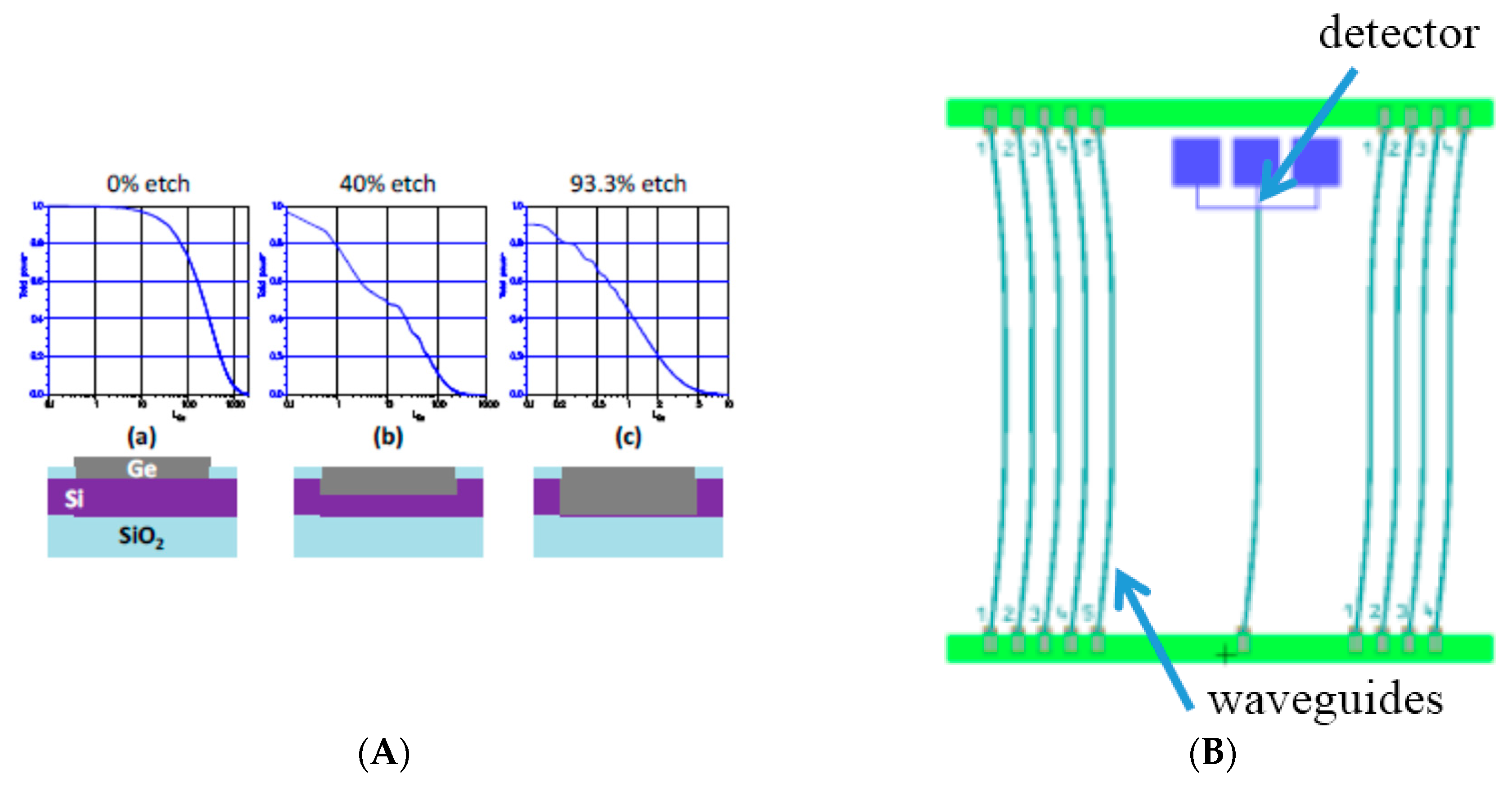
The micron-scale waveguides used in this work have a much stronger vertical confinement of the light compared to submicron silicon waveguides. Therefore, we simulated how much this confinement can affect the absorption length in the Ge detector. This is shown by the plot in Figure 2A, which indicates that more than 1 mm long detector would be needed to completely detect the incoming light in the case the Ge detector is placed above the waveguide. A second option could be the use of the silicon etch step defining the rib waveguides, which etches away 40% of the 3 μm thick SOI, as shown in the cross section in Figure 2A. Unfortunately also this option would still require hundreds of microns long detectors, which is unacceptable, given that detection speed and dark current scale inversely with the detector volume. The only way to make the detector sensibly shorter is to etch the silicon almost completely and just leave a few hundreds of nanometers thick pedestal as a seed for the Ge growth, similar to what reported in the literature of micron-scale SOI photodetectors [4]. In the example shown in Figure 1a, only 200 nm of Si are left, which makes possible to make a good detector shorter than 10 μm.
The layout of the die prepared to fabricate the devices is shown in Figure 2B. Test waveguides have been added to the design to estimate the coupling losses in our chips and estimate therefore the responsivity of the detectors. At the end of the central waveguide we placed a cavity (that will be filled up with SiGe during processing and etched leaving 200 nm at the bottom). The die shown in Figure 2B is repeated 52 times across the wafer. Some variation in the way the cavity is made has been also implemented (tilt up to 5 degrees to avoid back reflection).
3. Fabrication
The devices have been fabricated on a SOI wafer with a 3 μm top silicon layer and a 3 μm Buired Oxide (BOX). First, a boron implantation (10^14, 10 keV) through a 20 nm of thermal oxide is performed to create connection with the bottom (anode) of the SiGe. The dopants are activated by an annealing step for 1 hour at 1100 °C. Then, the waveguides and detector cavities (5 μm × 5 μm) are simultaneously etched into the top silicon layer of the SOI wafer using Deep Reactive Iion Etching (DRIE) leaving 200 nm of Si, Figure 3a. The SiGe growth takes then place in a xxx rector. Three steps of 15 min deposition each are used with a reactor clean in between. The SiGe is capped using a 10 nm p-type doped Si layer to prevent the SiGe to be damaged during the following process steps and to create an ohmic contact on the top of the SiGe, followed by a contact opening on the doped region. A 2 μm-thick Al/Si is applied and patterned to contact the top of the Ge and the two doped regions, Figure 3b.
4. Results
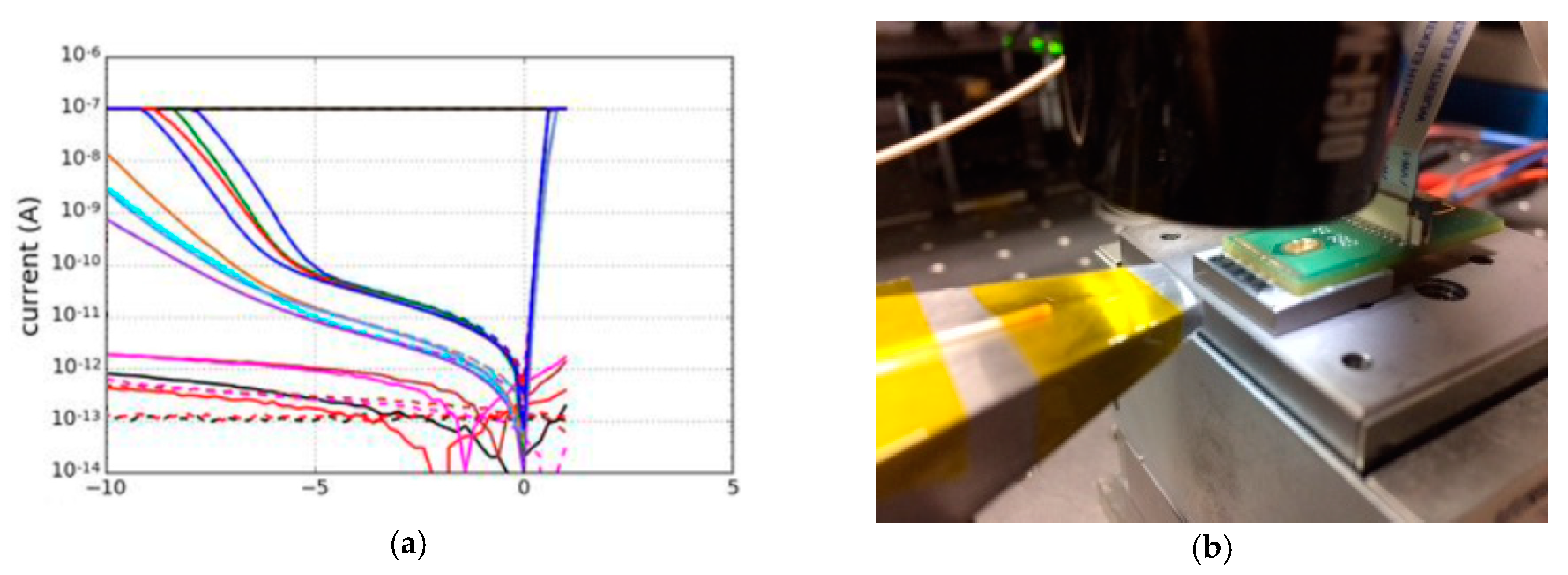
The wafers containing the devices were automatically measured on a probe station. Forward current measurements between 0 and 1 V were at first performed to confirm the diode behavior of the devices. To assess the dark current the voltage was then varied between 0 and −10 V. The results are shown in Figure 5a, indicated values lower than 0.1 nA. These values are much lower than those reported in [5,6], Table 1.
The devices were then packaged using a PCB board and the responsivity was assessed by measuring the difference in current observed for different light intensities, Figure 5b. The coupling losses were estimated using the straight waveguides present on the die. Those waveguides exhibit a total loss of 4 dB. An Exalos source provides the 1.3 μm incoming light. The lower responsivity measured with the current device is most likely due to the defects induced during the first 200 nm of the growth. A possible way to address this issue would be to use higher growth temperature to limit defects.
5. Conclusions
A fabrication process flow has been carried out successfully to test the design of monolithically integrated Ge photodetectors. Measured dark current levels are perfectly suitable for real applications, but responsivity is found lower than the state of the art, most likely due too many Ge defects. In fact, too much roughness on the areas where Ge is grown the limits Ge quality, as well growth of Ge on the edges of the growth pits. Clear paths to improve Ge quality have been identified and further measurements on speed will be now carried out.
Acknowledgments
This work has been supported by the Europen Project FP7 ICP 611132. The authors are grateful towards the Else Kooi Laboratory team for their extensive support.
Conflicts of Interest
The authors declare no conflict of interest.
References
- Abdulla, S.M.C.; de Boer, B.M.; Pozo, J.M.; van den Berg, J.H.; Abutan, A.; Hagen, R.A.J.; Harmsma, P.J. Sensing platform based on micro-ring resonator and on-chip reference sensors in SOI. Proc. SPIE 2014, 89900W-1. [Google Scholar] [CrossRef]
- Jovic, A.; Pandraud, G.; Sanchez, N.; Sancho, J.; et al. Two novel MEMS actuators for self aligned 3D optical coherent tomography. In Proceedings of the 2017 IEEE 30th International Conference on Micro Electro Mechanical Systems (MEMS), Las Vegas, NV, USA, 22–26 January 2017; pp. 797–800. [Google Scholar] [CrossRef]
- Feng, D.; Liao, S.; Dong, P.; Feng, N.N.; Liang, H.; Zheng, D.; Krishnamoorthy, A.V. High-speed Ge photodetector monolithically integrated with large cross-section silicon-on-insulator waveguide. Appl. Phys. Lett. 2009, 95. [Google Scholar] [CrossRef]
- Vivien, L.; Osmond, J.; Fedeli, J.M.; Marris-Morini, D.; Crozat, P.; Damlencourt, J.F.; Laval, S. 42 GHz pin Germanium photodetector integrated in a silicon-on-insulator waveguide. Opt. Express 2009, 17, 6252–6257. [Google Scholar] [CrossRef] [PubMed]
- Verheyen, P.; Lepage, G.; Van Campenhout, J.; Pantouvaki, M.; Absil, P.; De Heyn, P.; Dumon, P. Co-integration of Ge detectors and Si modulators in advanced Si photonics platform. Proc. SPIE Int. Soc. Opt. Eng. 2012, 8431, 8431–8439. [Google Scholar]
- Kang, Y.; Liu, H.D.; Morse, M.; Paniccia, M.J.; Zadka, M.; Litski, S.; Zaoui, W.S. Monolithic germanium/silicon avalanche photodiodes with 340 GHz gain–bandwidth product. Nat. Photonics 2009, 3, 59–63. [Google Scholar] [CrossRef]
Figure 1.
Standalone optical sensors: (a) The conventional approach with a optimized couplers to the source and the detector; (b) The approach where the source and the detector are integrated.
Figure 1.
Standalone optical sensors: (a) The conventional approach with a optimized couplers to the source and the detector; (b) The approach where the source and the detector are integrated.

Figure 2.
(A) Simulated transmission vs detection length and SiGe position: (a) SiGe on top of waveguide; (b) SiGe halfway in Si; (c) SiGe on 200nm Si left in the cavity; (B) The layout of the chip with the central waveguide terminating by a SiGe detector and the peripheral test waveguides.
Figure 2.
(A) Simulated transmission vs detection length and SiGe position: (a) SiGe on top of waveguide; (b) SiGe halfway in Si; (c) SiGe on 200nm Si left in the cavity; (B) The layout of the chip with the central waveguide terminating by a SiGe detector and the peripheral test waveguides.

Figure 3.
(a) Waveguide definition with the cavity for the SiGe growth; (b) A detector with the metal connections.
Figure 3.
(a) Waveguide definition with the cavity for the SiGe growth; (b) A detector with the metal connections.

Figure 4.
(a) Waveguide end facets to ease the coupling into the waveguide; (b) A fabricated detector with the metal connections.
Figure 4.
(a) Waveguide end facets to ease the coupling into the waveguide; (b) A fabricated detector with the metal connections.

Figure 5.
(a) I-V curves of 15 devices measured across the wafer; (b) A die after wire bonding placed on an optical bench for testing.
Figure 5.
(a) I-V curves of 15 devices measured across the wafer; (b) A die after wire bonding placed on an optical bench for testing.


Publisher’s Note: MDPI stays neutral with regard to jurisdictional claims in published maps and institutional affiliations. |
© 2017 by the authors. Licensee MDPI, Basel, Switzerland. This article is an open access article distributed under the terms and conditions of the Creative Commons Attribution (CC BY) license (https://creativecommons.org/licenses/by/4.0/).
Share and Cite
MDPI and ACS Style
Pandraud, G.; Milosavljevic, S.; Sammak, A.; Cherchi, M.; Jovic, A.; Sarro, P. Integrated SiGe Detectors for Si Photonic Sensor Platforms. Proceedings 2017, 1, 559. https://doi.org/10.3390/proceedings1040559
AMA Style
Pandraud G, Milosavljevic S, Sammak A, Cherchi M, Jovic A, Sarro P. Integrated SiGe Detectors for Si Photonic Sensor Platforms. Proceedings. 2017; 1(4):559. https://doi.org/10.3390/proceedings1040559
Chicago/Turabian StylePandraud, Grégory, Silvana Milosavljevic, Amir Sammak, Matteo Cherchi, Aleksandar Jovic, and Pasqualina Sarro. 2017. "Integrated SiGe Detectors for Si Photonic Sensor Platforms" Proceedings 1, no. 4: 559. https://doi.org/10.3390/proceedings1040559