Thermal Noise Limited, Scalable Multi-Piezoresistor Readout Architecture †


1
Institute of Technical Physics and Materials Science, Centre for Energy Research, HAS, H-1121 Budapest, Hungary
2
Doctoral School on Material Sciences and Technologies, Óbuda University, H-1034 Budapest, Hungary
*
Author to whom correspondence should be addressed.
†
Presented at the Eurosensors 2017 Conference, Paris, France, 3–6 September 2017.
Proceedings 2017, 1(4), 598; https://doi.org/10.3390/proceedings1040598
Published: 11 August 2017
(This article belongs to the Proceedings of Proceedings of Eurosensors 2017, Paris, France, 3–6 September 2017)
Abstract
:In this work we present a low noise, hardware efficient, and scalable read-out architecture for piezoresistive mechanical transducers containing multiple sensing elements. To reach the thermal noise limit the sensing elements are driven by modulated, differential stimuli at separated frequencies, their current are summed and digitalized for signal processing and response extraction. The solution decreases the complexity of the analog read-out electronics and makes it easily scalable. Besides the improved signal-to-noise ratio the principle can achieve minimised power consumption and self-heating of piezoresistors with minimal analogue hardware resources. The distinguishing features of the arrangement are the multiple frequency modulation, the current based multiple sensor integration, one AD converter, no analog multiplexing, and the need for only a half Wheatstone bridge per sensing element.
1. Introduction
The resolution of the piezoresistive cantilever or membrane deformation based mechanical sensors are limited electrically by the Johnson or thermal noise, shot noise, generation-recombination noise and the Hooge noise (. The frequency-independent thermal noise and the low-frequency noise are the dominant effects. The thermal noise amplitude becomes larger than the noise after a typically kHz range threshold frequency, thus using higher frequency modulated AC signal stimuli the noise can be supressed as common in lock-in amplification. Though the sensitivity (electrical response over deformation) can be increased by the increasing current flowing through the resistors and make use its voltage drop in parallel the 1/f noise and the threshold frequency also increases [1].
2. Materials and Methods
Our solution based on AC modulation scheme as well, with the extension of dedicating an individual frequency channel for each piezoresistive element (Figure 1).
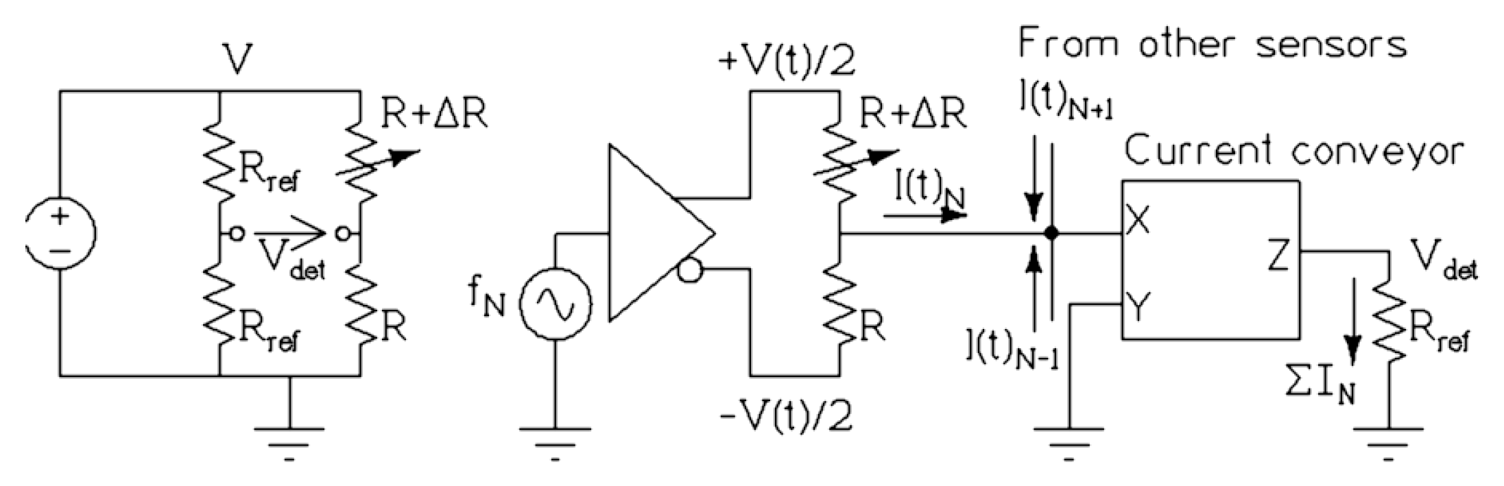
In order to minimize the hardware resources (namely the area consuming AD converter), the current flowing through the resistor elements is summed using a current conveyor circuit and then digitalized by a single AD converter. The modulation uses square wave waveform to decrease the hardware complexity further (Figure 2).
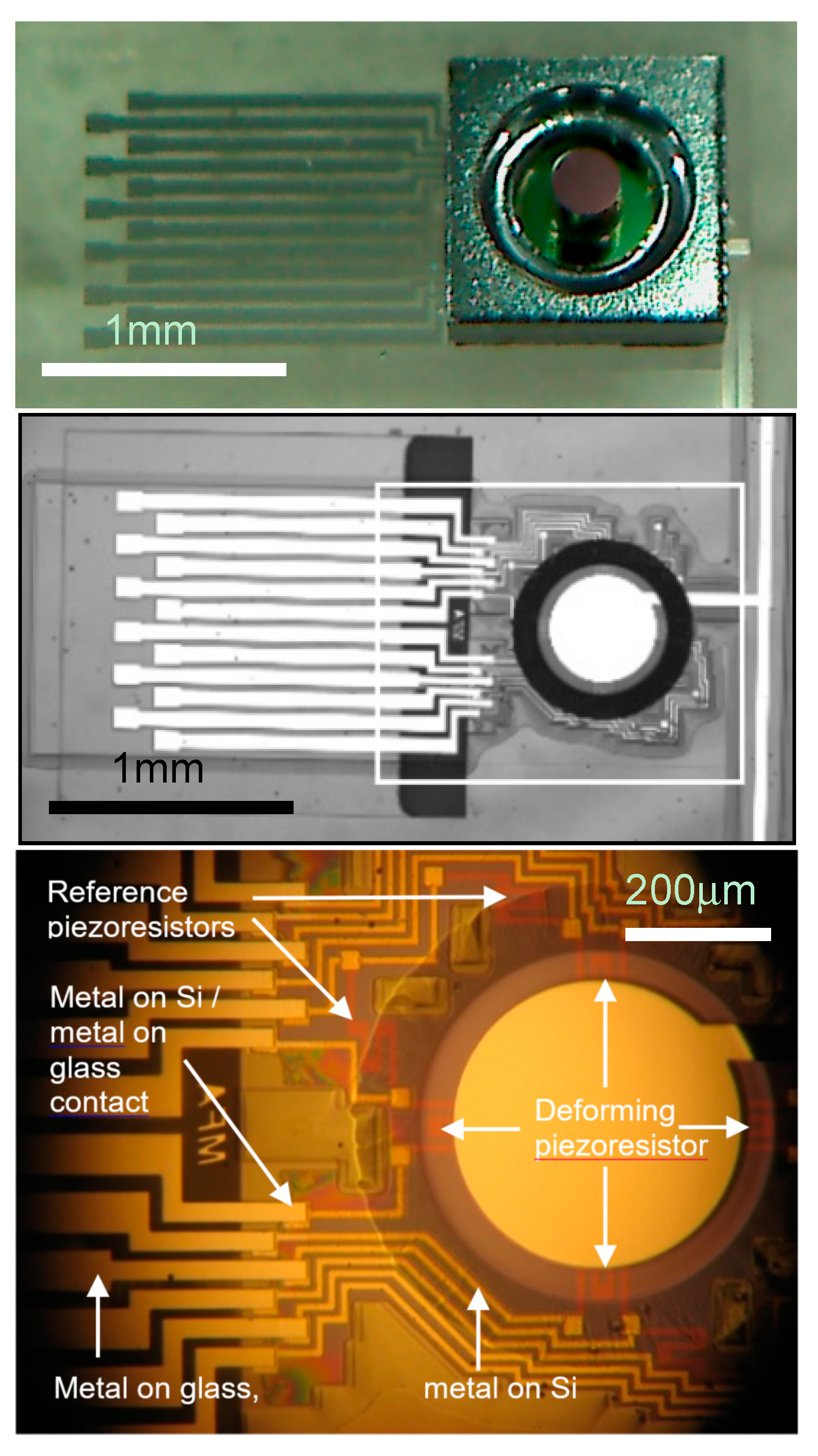
The signal stream is processed to derive the individual responses of the sensing elements. In order to eliminate the manufacturing mismatches of the piezoresistive elements, the solution uses a half Wheatstone bridge. To limit the accumulated current value of the half bridges a differential signal drives the resistor pairs with forcing the half voltage level by a current conveyor. This way only the resistance change related current flows to the summing node. The demonstration system based on a four element force sensor (Figure 3) fabricated on SOI wafers by using typical processes as doping implantation, DRIE etching, anodic wafer bonding to borosilicate glass containing wiring [2].
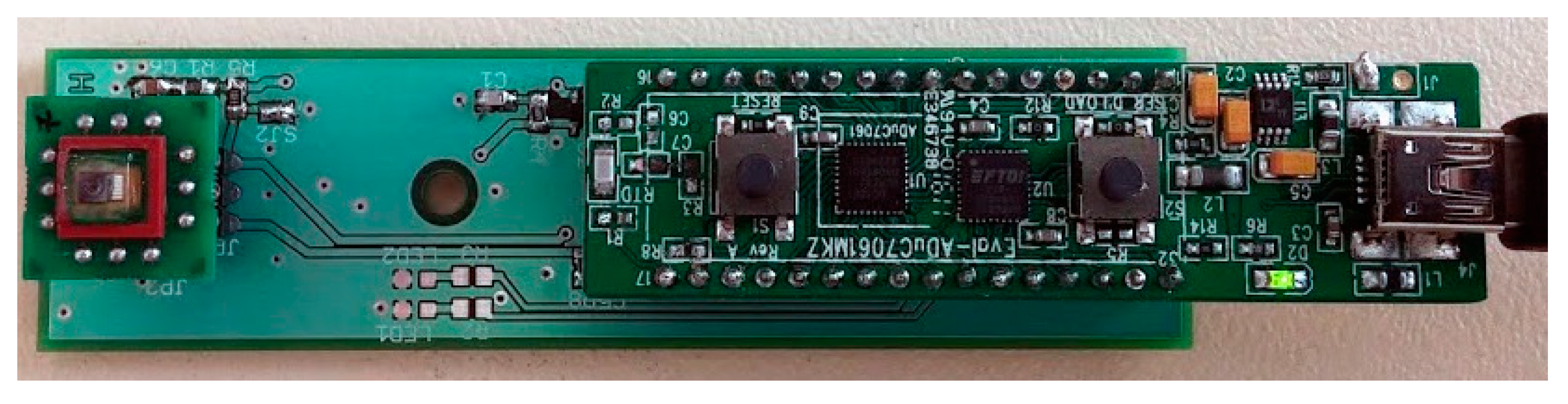
The electronics contains solely a 16-bit ARM processor based microcontroller including 24-bit sigma-delta converter (Analog devices, ADuC7061) with supporting elements (Figure 4).
3. Results and Conclusions
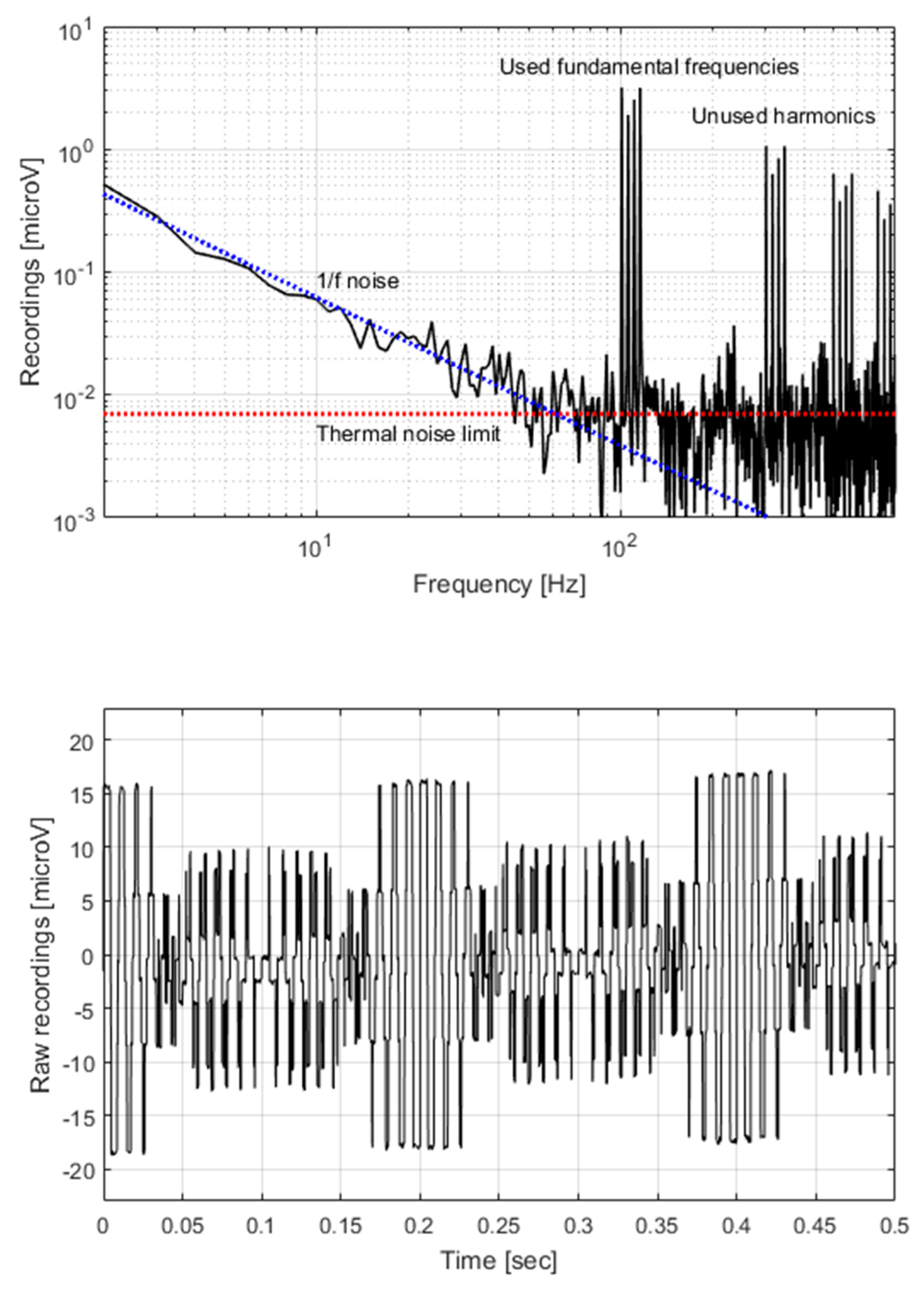
Typical noise and time domain signal is demonstrated in Figure 5. At the applied frequencies (200, 210, 220 and 230 Hz) the demodulated voltage changes was in the range of 3–5 µV, the noise floor is near 8–9 (piezoresistor is 3.6 ), the modulation was ±0.6 V and one second sample time. The mechanically upper limited SNR is 100 dB.
Acknowledgments
This work was done in the frame of the ENIAC “INCITE” project No. 621278 jointly financed by the ENIAC JU and the National Research, Development and Innovation Fund (NKFIA) via NEMZ_12-1-2014-0005. The work was partially supported by the NKFIA via 109674 and NVKP_16-1-2016-0018 grants also. Péter Földesy acknowledges the support of János Bólyai Scholarship of the Hungarian Academy of Sciences. Special thanks to Attila Nagy for assembly of the test devices.
Conflicts of Interest
The authors declare no conflict of interest. The founding sponsors had no role in the design of the study; in the collection, analyses, or interpretation of data; in the writing of the manuscript, and in the decision to publish the results.
References
- Xiaomei, Y.; Thaysen, J.; Hansen, O.; Boisen, A. Optimization of sensitivity and noise in piezoresistive cantilevers. J. Appl. Phys. 2002, 92, 6296–6301. [Google Scholar] [CrossRef]
- Radó, J.; Dücső, C.; Battistig, G.; Szebényi, G.; Fürjes, P.; Nawrat, Z.; Rohr, K. 3D force sensors for laparoscopic surgery tool. In Proceedings of the Design, Test, Integration and Packaging of MEMS/MOEMS—DTIP 2016 Conference, Budapest, Hungary, 30 May–2 June 2016; IEEE XPlore 7514829. [Google Scholar] [CrossRef]
Figure 1.
Concept of the standard Wheatstone bridge (left) and the described differential AC driven, current summed architecture (right).
Figure 1.
Concept of the standard Wheatstone bridge (left) and the described differential AC driven, current summed architecture (right).

Figure 2.
Practical system architecture with binary modulation and signal processing components.

Figure 3.
Vectorial piezoresistive force sensor (top). Optical views of wafer bonded chips as looking from the glass side (middle and bottom): overviews and magnified part of the active area. The auxiliary metal circles on the glass partially cover the Si membranes underneath.
Figure 3.
Vectorial piezoresistive force sensor (top). Optical views of wafer bonded chips as looking from the glass side (middle and bottom): overviews and magnified part of the active area. The auxiliary metal circles on the glass partially cover the Si membranes underneath.

Figure 4.
Test setup can be seen with the force sensor on the left covered by protecting silicon rubber and the supporting microcontroller among its peripheries on the right side.
Figure 4.
Test setup can be seen with the force sensor on the left covered by protecting silicon rubber and the supporting microcontroller among its peripheries on the right side.

Figure 5.
Four piezoresistive (thus four frequencies) setup with FFT plot (top) and time domain signal (bottom). Binary modulation frequencies was 200 Hz, 210 Hz, 220 Hz and 230 Hz. Signal levels are 3–5 µV, noise floor is near 8 for the sensing element of 3.6 , the measurement time was 1 s. The applied modulation voltage is ±0.6 V, the applicable force SNR of the sensor, constraint mechanically by sensor damage, is near 100 dB with the setup.

Publisher’s Note: MDPI stays neutral with regard to jurisdictional claims in published maps and institutional affiliations. |
© 2017 by the authors. Licensee MDPI, Basel, Switzerland. This article is an open access article distributed under the terms and conditions of the Creative Commons Attribution (CC BY) license (https://creativecommons.org/licenses/by/4.0/).
Share and Cite
MDPI and ACS Style
Radó, J.; Battistig, G.; Pap, A.E.; Fürjes, P.; Földesy, P. Thermal Noise Limited, Scalable Multi-Piezoresistor Readout Architecture. Proceedings 2017, 1, 598. https://doi.org/10.3390/proceedings1040598
AMA Style
Radó J, Battistig G, Pap AE, Fürjes P, Földesy P. Thermal Noise Limited, Scalable Multi-Piezoresistor Readout Architecture. Proceedings. 2017; 1(4):598. https://doi.org/10.3390/proceedings1040598
Chicago/Turabian StyleRadó, János, Gábor Battistig, Andrea Edit Pap, Péter Fürjes, and Péter Földesy. 2017. "Thermal Noise Limited, Scalable Multi-Piezoresistor Readout Architecture" Proceedings 1, no. 4: 598. https://doi.org/10.3390/proceedings1040598