Proceeding Paper

High Sensitivity Piezogenerator Based on GaN Nanowires †

1
Centre de Nanosciences et de Nanotechnologies-site Orsay, University Paris-Saclay, Bât. 220-Centre Scientifique d’Orsay, F-91405 Orsay, France
2
Centre de Nanosciences et de Nanotechnologies-site Marcoussis, University Paris-Saclay, Route de Nozay, F-91460 Marcoussis, France
3
GeePs, UMR 8507 CNRS-Centrale Supélec, University Paris-Sud et UPMC, 91192 Gif-sur-Yvette, France
*
Author to whom correspondence should be addressed.
Presented at the Eurosensors 2017 Conference, Paris, France, 3–6 September 2017.
Proceedings 2017, 1(4), 587; https://doi.org/10.3390/proceedings1040587
Published: 7 August 2017
(This article belongs to the Proceedings of Proceedings of Eurosensors 2017, Paris, France, 3–6 September 2017)

Abstract

:
We report on a prototype of piezogenerator based on vertically-aligned GaN nanowires grown by Plasma-Assisted Molecule Beam Epitaxy (PAMBE). Our device generates a peak-to-peak voltage from 20 mV to 60 mV depending on the applied force. The output power density reaches 0.76 mW/cm3 which is of the same order of magnitude as the state-of-art value. Furthermore, the pressure applied to deform the nanowires is of the order of kPa, much less than that used in previous reports (which were of the order of MPa) utilizing ZnO nanowires for the power generation. Thus, an enhanced mechanic-electrical conversion efficiency has been achieved. Our GaN nanowire based devices are promising both for pressure sensing applications and for mechanic energy harvesting.

1. Introduction

Today, the independent powering of nomad electronic devices still remains a challenge. Generators based on piezoelectric nanowires offer the possibility of converting ambient mechanical energy into usable electrical energy, which enables the realization of ultra compact power sources to meet this need.
The piezogeneration potential of ZnO nanowires has been widely studied in the past years, and various integrated devices have been fabricated. However, the mechanic-electrical conversion efficiency of the devices remains low since rather high external force has to be applied to generate an electrical response [1]. GaN nanowires have a higher piezoelectric coefficient compared to ZnO nanowires at the same size scale [2]. At the same time, they yield a higher single-nanowire piezogeneration, as demonstrated experimentally by Gogneau et al. [3]. In this work, we use GaN nanowires to fabricate piezogenerators producing electricity under small external forces.

2. Nanowire Growth

The GaN nanowires used for piezogenerator fabrication were grown by plasma-assisted molecular beam epitaxy. At first, a thin n-doped AlN buffer layer is deposited on a n-type doped Si (111) substrate to ensure nanowire verticality [4]. This ultra-thin layer is doped and presents a good electrical conductivity, allowing the nanowires to be electrically connected to the Si substrate. Then the growth of GaN nanowires is performed under nitrogen-rich conditions at a substrate temperature of 790 °C. Nanowires are characterized by a cylindrical shape and a hexagonal cross section. The nanowires mostly exhibit N-polarity. They have a height of the order of 1.45 µm ± 107 nm, a diameter of 47 nm ± 16 nm and a density of the order of 109 NWs/cm² (Figure 1). The nanowire morphology is illustrated in Figure 1, displaying cross-sectional and top-view SEM images.

3. Device Fabrication

To fabricate the devices, the as grown nanowire arrays are encapsulated into diluted PDMS. PDMS can penetrate between the nanowires filling uniformly the empty space, then it is annealed for 1 h at 80 °C. With this encapsulation, nanowires in the device are fully separated and electrically isolated while their orientation is well preserved. Then the nanowire tops are uncovered by doing reactive ion etching (RIE) and the Cr/Pt top Schottky contacts are deposited though a shadow-mask. The size of the contact pad is 3.14 mm2. Finally, an ohmic contact is directly deposited on the substrate serving as a back contact. The device schematic is shown in Figure 2.

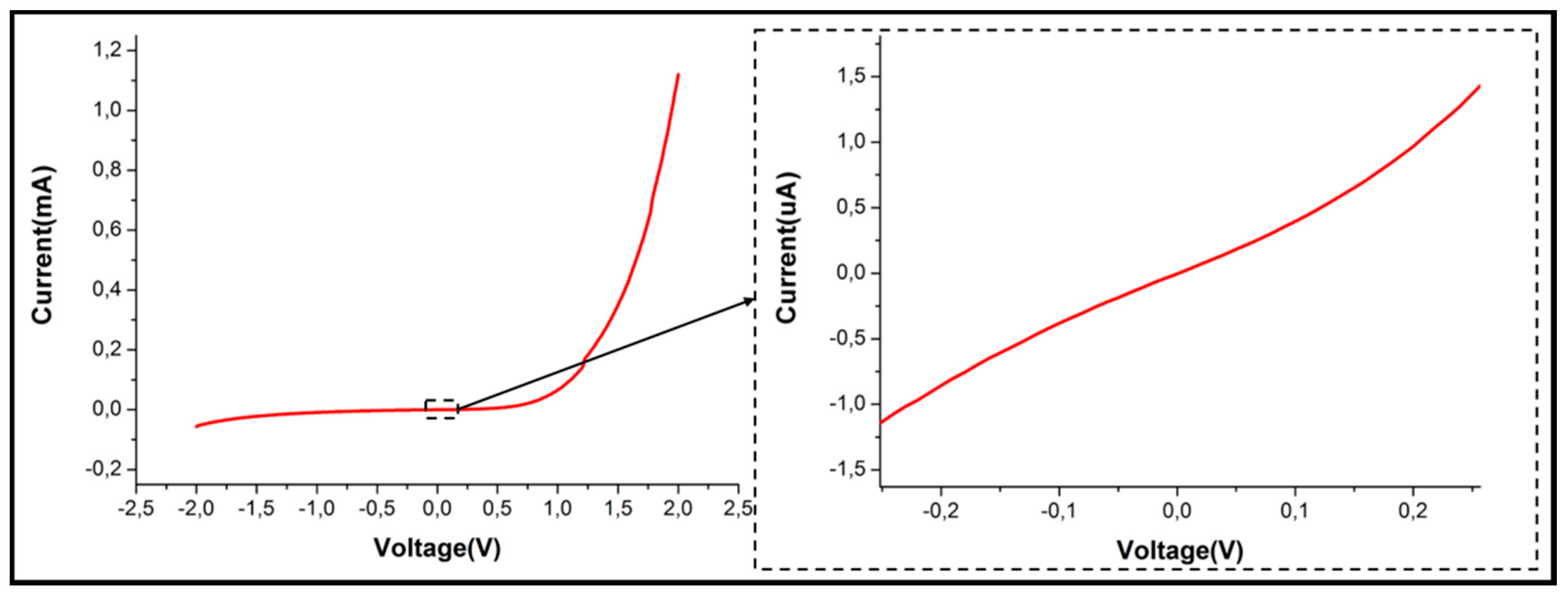
4. Device Performance

Firstly, the I-V curve of the device is measured. We observe a rectifying behavior which confirms the good quality of the Schottky top contact (Figure 3). The resistance of one contacted region is about 0.3 MΩ.
We then use an isolated shaker head (1 mm diameter) to apply a controllable force on the device top contact at a given frequency (from 1 Hz to 50 Hz). In this way, the nanowire array under the shaker head is compressed and released uniformly along the growth c-axis direction. Figure 4 shows the voltage generated by the device at a tapping frequency of 30 Hz. A generation voltage up to 25 mV is observed in this measurement.
The device is connected to an oscilloscope with a load resistance of 1 MΩ. To calculate the output power, we use the formula:
P = U 2 / R
where R = 1 MΩ and U = 30 mV, the maximum peak output voltage.
The effective volume of the active material is calculated as:
V = π r 2 h
where r = 0.5 mm is defined by the diameter of the shaker head, h = 1.5 μm is the height of the nanowire array. In this way, the output power density is estimated as 0.76 mW/cm3. This value is of the same order as the present state of art value [5]. Besides, by controlling the applied force of the shaker, the pressure added onto the device during the whole measurement process is in the order of kPa. Compared to existing reported results, our device has an enhanced mechanical-electrical conversion efficiency for small applied force. Therefore, it is suitable for conversion of small ambient deformations.

5. Conclusions

In this work, we embed vertical self-assembled GaN nanowires grown by PA-MBE on Si (111) substrate into PDMS to fabricate piezogenerators. By compressing and releasing vertically the nanowire array along their c-axis direction, we observe a piezogeneration with a peak-to-peak voltage ranging from 20 mV to 60 mV. An output power density of 0.76 mW/cm3 is estimated at a pressure of the order of kPa. The strong response under low external pressure received shows the good mechanical-electrical converting capability of our device. Therefore the device is promising for future applications not only as a generator, but also as a sensitive pressure sensor.

Acknowledgments

The financial support from the H2020 ERC project NanoHarvest is acknowledged.

Conflicts of Interest

The authors declare no conflict of interest.

References

  1. Xu, S.; Qin, Y.; Xu, C.; Wei, Y.; Yang, R.; Wang, Z.L. Self-powered nanowire devices. Nat. Nanotechnol. 2010, 5, 366–373. [Google Scholar] [CrossRef] [PubMed]
  2. Agrawal, R.; Espinosa, H.D. Giant Piezoelectric Size Effects in Zinc Oxide and Gallium Nitride Nanowires. A First Principles Investigation. Nano Lett. 2011, 11, 786–790. [Google Scholar] [CrossRef] [PubMed]
  3. Gogneau, N.; Chrétien, P.; Galopin, E.; Guilet, S.; Travers, L. Impact of the GaN nanowire polarity on energy harvesting. Appl. Phys. Lett. 2014, 104, 213105. [Google Scholar] [CrossRef]
  4. Largeau, L.; Galopin, E.; Gogneau, N.; Travers, L.; Glas, F.; Harmand, J.-C. N-Polar GaN Nanowires Seeded by Al Droplets on Si (111). Cryst. Growth Des. 2012, 12, 2724. [Google Scholar] [CrossRef]
  5. Jamond, N.; Chrétien, P.; Houzé, F.; Lu, L.; Largeau, L.; Maugain, O.; Travers, L.; Harmand, J.C.; Glas, F.; Lefeuvre, E.; et al. Piezo-generator integrating a vertical array of GaN nanowires. Nanotechnology 2016, 27, 325403. [Google Scholar] [CrossRef] [PubMed]
Figure 1. SEM images (cross section and top view) of the as-grown GaN nanowires.
Proceedings 01 00587 g001
Figure 2. Schematic of the piezogenerator, integrating vertically aligned GaN nanowires.
Proceedings 01 00587 g002
Figure 3. I-V characterization shows a Schottky behavior of the top contact (right: zoom of the low voltage range).
Proceedings 01 00587 g003
Figure 4. Generated voltage of the device measured at a compressing rate of 30 Hz (zoom of one period on the right).
Proceedings 01 00587 g004
Publisher’s Note: MDPI stays neutral with regard to jurisdictional claims in published maps and institutional affiliations.

