2D In-Plane Sensitive Hall-Effect Sensor †


Institute of Robotics at Bulgarian Academy of Sciences, 1113 Sofia, Bulgaria
*
Author to whom correspondence should be addressed.
†
Presented at the Eurosensors 2018 Conference, Graz, Austria, 9–12 September 2018.
Proceedings 2018, 2(13), 711; https://doi.org/10.3390/proceedings2130711
Published: 30 November 2018
(This article belongs to the Proceedings of EUROSENSORS 2018)
Abstract
:A new 2D (two-dimensional) in-plane sensitive Hall-effect sensor comprising two identical n-Si Greek-crosses is presented. Each of the crosses contains one central square contact and, symmetrically to each of their four sides, an outer contact is available. Outer electrode from one configuration is connected with the respective opposite contact from the other configuration, thus forming four parallel three-contact (3C) Hall elements. These original connections provide pairs of opposite supply currents in each of the cross-Hall structure. Also the obligatory load resistors in the outer contacts of 3C Hall elements are replaced by internal resistances of crosses themselves. The samples have been implemented by IC technology, using four masks. The magnetic field is parallel to the structures’ plane. The couples of opposite contacts of each Greek-cross are the outputs for the two orthogonal components of the magnetic vector at sensitivities S ≈ 115 V/AT whereas the cross-talk is very promising, reaching no more than 2.4%. The mean lowest detected magnetic induction B at a supply current Is = 3 mA over the frequency range f ≤ 500 Hz at a signal to noise ratio equal to unity, is Bmin ≈ 14 μT.
1. Introduction
The measurement of more than one orthogonal component of magnetic field vector using single-chip approach is the most advanced problem in the multidimensional microsystems. This method provides advantages as high spatial resolution and minimal operational volume, drastically improved orthogonality between the two or three axes, the position of the device with respect to the magnetic source is not critical, very good electrical, thermal and galvanomagnetic compatibility in individual sensor channels etc. The most advanced 2D and 3D vector configurations use the Hall effect, since their action involves only one simple, well-defined and well-investigated physical principle, [1,2,3,4,5,6,7,8]. These microsensors, irrespective of the pronounced progress, with respect to channel sensitivities, cross-talk, technology compatibility etc. feature some essential drawbacks. They contain too many contacts and numerous electrical connections between them, which seriously complicates fabrication, impedes minimal operational volume and obstructs the required miniaturization degree. Also there are unsatisfactory solutions for overcoming the sensitivity temperature dependence, drift and channel offsets. The relevant technologic realization of these disadvantages exceeds many times the simplicity of the Hall sensor itself. Another problem is the channel cross-talk which reduces the accuracy, [1,6,7,8]. An original CMOS multidimensional Hall magnetometer strictly measuring Bx and By in-plane components is given in [9]. Despite of its merits, the devise design is very complicated, containing four 3C in-plane Hall microsensors, similar to described ones in [10,11]. In this paper, a novel single-chip sensing device for measurement of two orthogonal in-plane magnetic-field components using simple construction, improved cross-talk and satisfactory resolution is presented.
2. Sensor Design and Operation Principle
The multidimensional device consists of two identical n-Si Greek-crosses, Figure 1. Each of them contains one central n+ square contact C1, C2. Symmetrically to each of their four sides, there is one n+ outer contact. Each outer terminal from a given configuration is connected to the respective opposite contact from the other arrangement, C3–C9, C4–C10, C5–C7 and C6–C8, thus forming four parallel 3C Hall elements.
These original connections provide pairs of opposite in direction supply currents in each of the cross-Hall structure. Also the obligatory load resistors in the outer contacts of 3C Hall elements [10,11] are replaced by internal resistances of cross-configurations themselves. A deep p-ring surrounding the Greek-crosses to restrict surface spreading currents and to confine the effective transducer zones within the n-Si substrate is formed, too, Figure 1.
The experimental prototype has been implemented using part of the processing steps applied in bipolar IC technology. The low-doped n-Si plates are 300 μm thick, with resistivity ρ ≈ 7.5 Ω·cm. The carrier’s concentration is n ~ 4.3 × 1015 cm−3. Similarly to [12], four masks are employed. Mask 1 determines the n+-implanted zones for ohmic electrical contacts C1 … C10 with the substrate, as the depth of the ohmic n+-n junctions is about 1 μm. Mask 2 forms areas for the two deep Greek-crosses p-rings. These p-rings constrict the effective volume of the device and prevent the surface current spreading. All of this increases the transducer efficiency of novel 2D device. Mask 3 defines the metallization layer and bonding pads. Mask 4 is intended for the contact opening in the surface layer SiO2 for the electrical contact between metal and the n+ zones. The dopant donor concentration of the n+-n junctions is n ≈ 1020 cm−3. The width of the deep surrounding p-ring at the surface is about 20 μm (on the mask). The size of the ohmic contacts is 30 × 30 μm2 for C1 and C2, and 30 × 10 μm2 for all the rest C3…C10. The distance between the central contacts and outer ones is 40 μm. The thickness of the effective area is defined in first approximation from the curvilinear trajectory penetration in the n-Si substrate with a depth of 30–40 μm. As a result, the effective operational volume of each cross is about 120 × 120 × 40 μm3, which provides for the satisfying spatial resolution of the device.
The current Is ≡ IC1,2 is constant in the 2D sensor, due to the high internal resistances as result from a few kilo ohms of the cross-configurations. The current paths start and end on the heavy-doped n+ contacts on the upper surface of the slab, thus the carriers’ trajectories are curvilinear. In magnetic field B(Bx, By) > 0, the Lorentz forces FL(FLx, FLy) influences the respective trajectories in the y-z and x-z planes. As a result forces FL(FLx, FLy) simultaneously shrink and expand the opposite paths in the two Greek-crosses towards the surfaces and to the bulks forming 3C in-plane sensitive Hall devices. Thus, opposite-sign Hall potentials are generated on the respective contacts. Through the circuitry connections, the potentials with the same sign are linked in parallel, forming the respective differential Hall outputs Vx(Bx) and Vy(By), Figure 1.
3. Results
The output characteristics for the Vx(Bx) channel of the new 2D magnetometer are shown in Figure 2, the dependence of the channel Vy(By) is the same. Inevitable offsets are fully compensated in advance. The obtained channel-magnetosensitivities are equal and reach SRI ≈ 115 V/AT at temperature T = 20 °C.
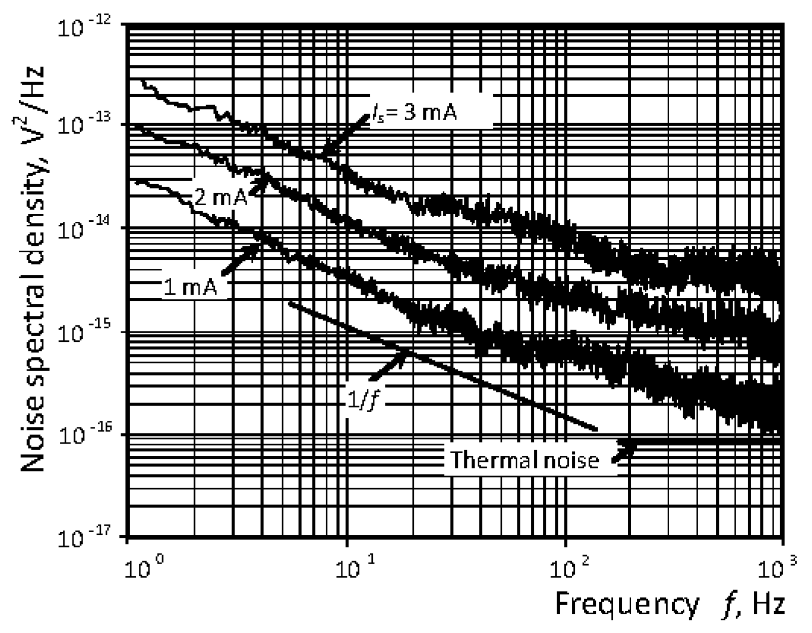
The non-linearity NL reaches no more 0.5% in the range 0 ÷ ± 0.6 T and NL ≈ 1% at ± 0.6 T ÷ ± 1.0 T. The main sensor characteristic in the vector magnetometry is the cross-sensitivity C.S. This important parameter determines the parasitic output signal in a given channel, when the field B is applied in the other orthogonal sensor direction. In Figure 3 the cross-talk i.e., the characteristic C.S. of 2D in-plane sensitive Hall sensor is presented as a function of induction B at temperature T = 20 °C. The experimental results are very promising, parameter C.S. reaches no more than 2.4%. The power spectral density of internal noise for the channel Vy(0) at T = 20 °C is demonstrated in Figure 4, the supply current Is is as a parameter. For the channel Vx(0) the noise density is the same. The dependencies are 1/f, if the supply Is increase, the noise 1/f augment too. The mean lowest detected magnetic induction B at a supply current Is = 3 mA over the frequency range f ≤ 500 Hz at a signal to noise ratio equal to unity, is Bmin ≈ 14 μT.
4. Conclusions
In summary the obtained performance of the novel 2D in-plane sensitive Hall device is very promising. This important result is achieved through simple in design innovative structure, original connections between contacts, possibility of simultaneous extraction of two independed channel voltages with drastically suppressed cross-talk between them, high inherent symmetry of the channels and simplified technology realization. The applications of the 2D sensor are wide—robotics, mechatronics, low-field magnetometry, position devices, multirotor systems, contactless automation etc.
Acknowledgments
This work was supported by Sci. Res. Fund under project No. DN 07/18-15.12.2016.
References
- Roumenin, C. Solid State Magnetic Sensors, Elsevier, 1994; Microsensors for magnetic field. In MEMS—A Practical Guide to Design, Analysis and Application; Korvink, J.G., Paul, O., Eds.; William Andrew Publisher: Norwich, NY, USA, 2006; pp. 453–521. [Google Scholar]
- Ramsden, E. Hall Effect Sensors—Theory and Application, 2nd ed.; Elsevier: Amsterdam, Netherland, 2006. [Google Scholar]
- Kaufmann, T. On the Offset and Sensitivity of CMOS-Based Five-Contact Vertical Hall Devices; Der Andere Verlag: Tonning, Germany, 2013; Volume 21, p. 147. [Google Scholar]
- Demierre, M.; Schurig, E.; Schott, C.; Besse, P.-A.; Popovic, R. Contactless 360° absolute angular CMOS microsystem based on vertical Hall sensors. Sens. Actuators A 2004, 116, 39–44. [Google Scholar] [CrossRef]
- Pascal, J.; Hebrard, L.; Frick, V.; Blonde, J.P. 3D Hall probe integrated in 0.35 um CMOS technology for magnetic field pulses measurements. In Proceedings of the 6th International IEEE Northeast Workshop on Circuits and Systems and TAISA 2008, Montreal, Quebec, Canada, 22–25 June 2008; pp. 97–100. [Google Scholar]
- Yu, C.-P. The Study and Application of a 2D Folded Hall Sensor Chip; National Taipei University of Technology: Taipei, Taiwan, 2012; p. 88. [Google Scholar]
- Yu, C.-P.; Sung, G.-M. Two-dimensional folded CMOS Hall device with interacting lateral magnetotransistor and magnetoresistor. Sens. Actuators A 2012, 182, 6–15. [Google Scholar] [CrossRef]
- Wouters, C.; Vranković, V.; Rössler, C.; Sidorov, S.; Ensslin, K.; Wegscheider, W.; Hierold, C. Design and fabrication of an innovative three-axis Hall sensor. Sens. Actuators A 2016, 237, 62–71. [Google Scholar] [CrossRef]
- Sander, C.; Leube, C.; Paul, O. Three-dimensional magnetometer based on subsequent measurement principle. Sens. Actuators A 2015, 222, 329–334. [Google Scholar]
- Roumenin, C.; Kostov, P. Planar Hall-Effect Device. Bulg. Patent No. 37208/26.12.1983, 26 December 1983. [Google Scholar]
- Lozanova, S.V.; Roumenin, C.S. Parallel-field silicon Hall effect microsensors with minimal design complexity. IEEE Sens. J. 2009, 9, 761–766. [Google Scholar] [CrossRef]
- Schott, C.; Popovic, R. Integrated 3-D Hall magnetic field sensor. In Proceedings of the Transducers ’99, Sendai, Japan, 7–10 June 1999; Volume 1, pp. 168–171. [Google Scholar]
Figure 1.
Schematic top-view of 2-D integrated Hall device. The simple design, original connection, inherent symmetry and deep p-ring drastically reduce the channels cross-talk and the offset is decreased too.
Figure 1.
Schematic top-view of 2-D integrated Hall device. The simple design, original connection, inherent symmetry and deep p-ring drastically reduce the channels cross-talk and the offset is decreased too.
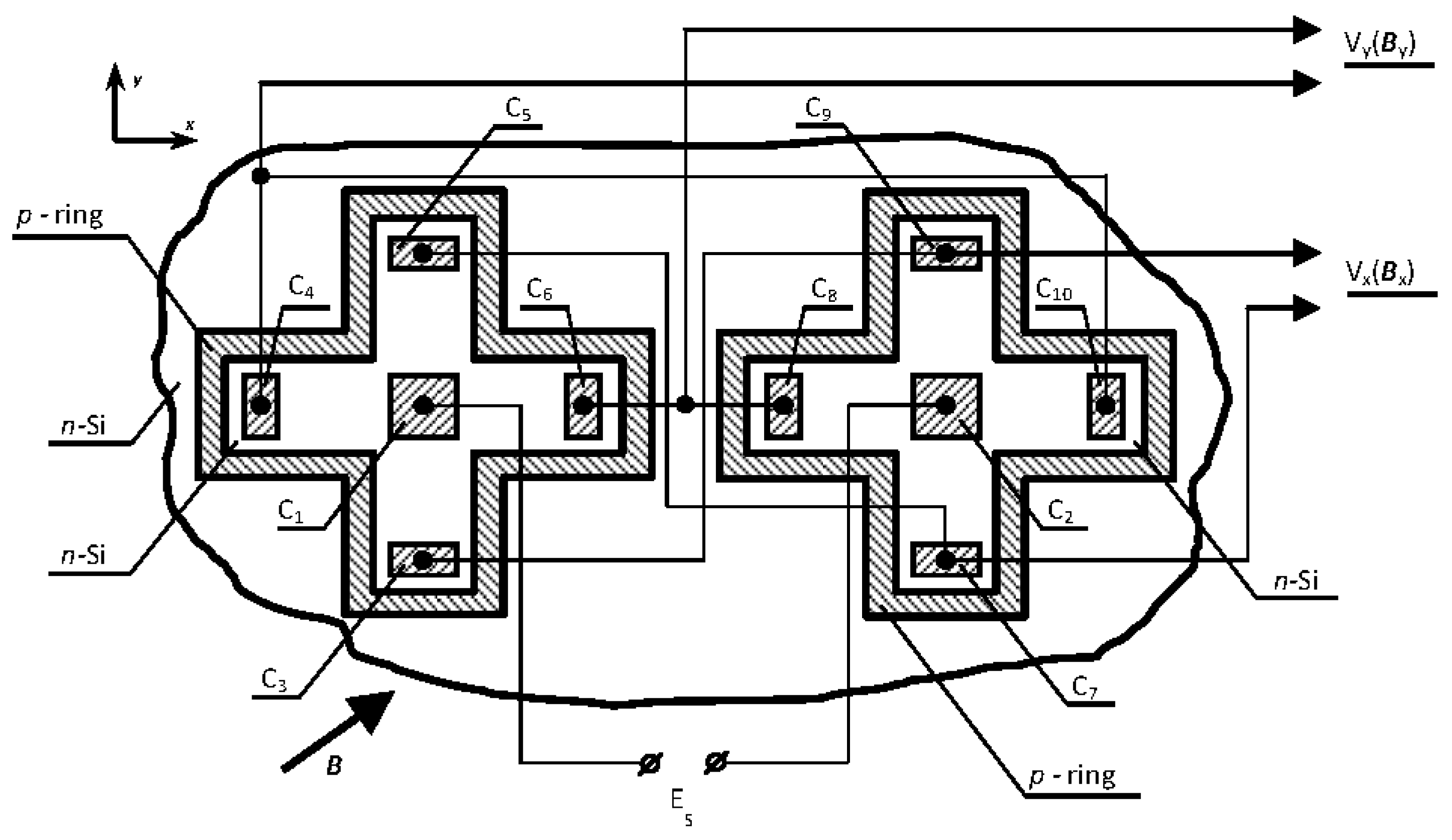
Figure 2.
Output characteristics for the Vx(B) channel of the new 2D device. The obtained magnetosensitivities are equal.
Figure 2.
Output characteristics for the Vx(B) channel of the new 2D device. The obtained magnetosensitivities are equal.
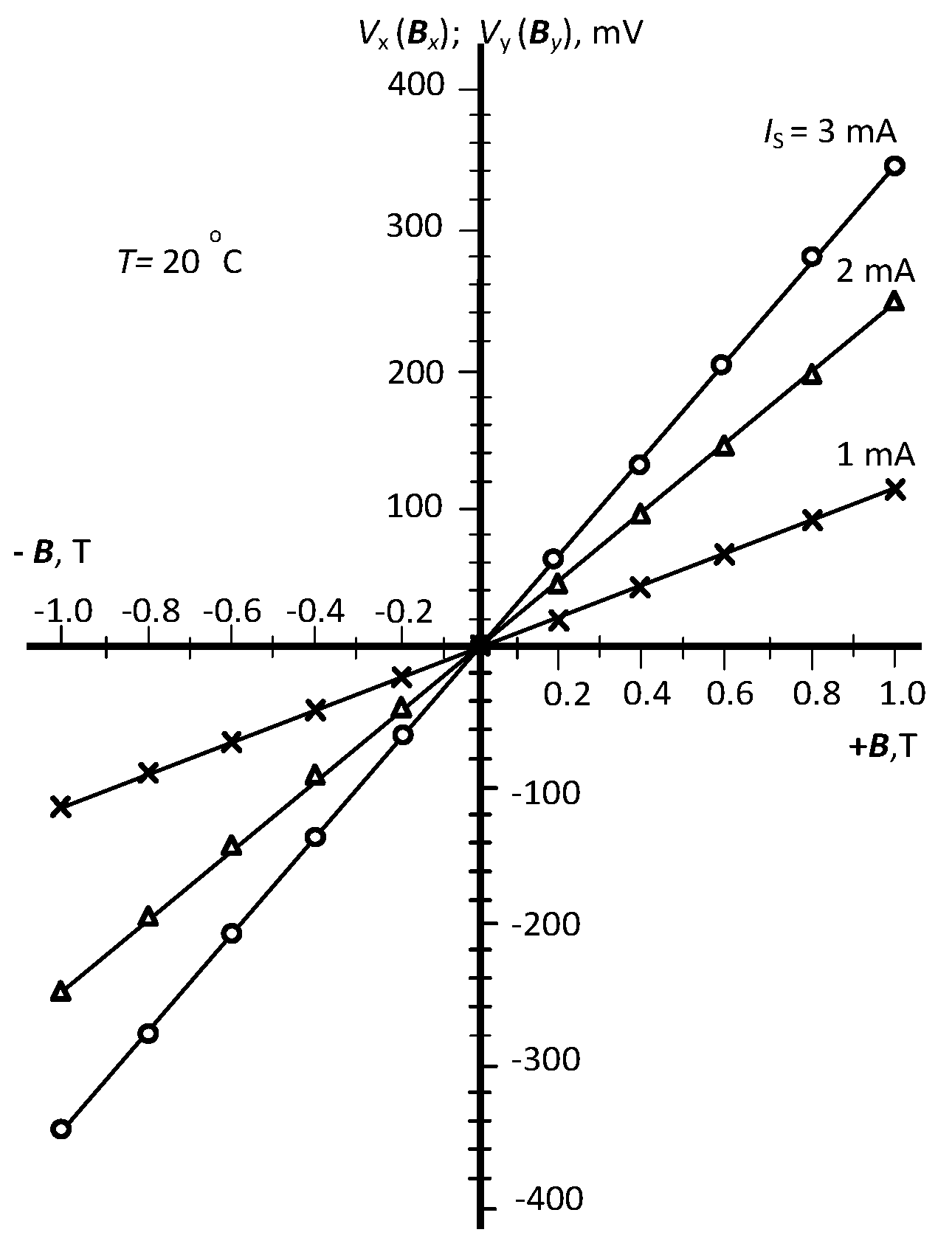
Figure 3.
Channel cross-talk of 2D in-plane sensitive Hall sensor as a function of induction B at temperature T = 20 °C.
Figure 3.
Channel cross-talk of 2D in-plane sensitive Hall sensor as a function of induction B at temperature T = 20 °C.
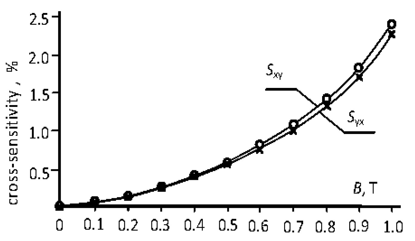
Figure 4.
Power spectral density of internal noise in channel Vy(0), the supply current Is is as a parameter, T = 20 °C.
Figure 4.
Power spectral density of internal noise in channel Vy(0), the supply current Is is as a parameter, T = 20 °C.
Publisher’s Note: MDPI stays neutral with regard to jurisdictional claims in published maps and institutional affiliations. |
© 2018 by the authors. Licensee MDPI, Basel, Switzerland. This article is an open access article distributed under the terms and conditions of the Creative Commons Attribution (CC BY) license (https://creativecommons.org/licenses/by/4.0/).
Share and Cite
MDPI and ACS Style
Lozanova, S.; Kolev, I.; Ivanov, A.; Roumenin, C. 2D In-Plane Sensitive Hall-Effect Sensor. Proceedings 2018, 2, 711. https://doi.org/10.3390/proceedings2130711
AMA Style
Lozanova S, Kolev I, Ivanov A, Roumenin C. 2D In-Plane Sensitive Hall-Effect Sensor. Proceedings. 2018; 2(13):711. https://doi.org/10.3390/proceedings2130711
Chicago/Turabian StyleLozanova, Siya, Ivan Kolev, Avgust Ivanov, and Chavdar Roumenin. 2018. "2D In-Plane Sensitive Hall-Effect Sensor" Proceedings 2, no. 13: 711. https://doi.org/10.3390/proceedings2130711